

1 Introduction
The covalent integration of self-assembled organic monolayers with semiconductor surfaces, such as silicon, constitutes a convenient strategy for achieving stable and high-quality hybrid junctions [1,2]. Furthermore, this covalent link should enhance the electronic transmission between the two components [3]. In the case where the organic structure is a redox-active material, such as an electronically conducting polymer, covalently bound to silicon via a long alkyl chain, it should be possible to create a large variety of molecular electronic devices (diodes, field-effect transistors, memories) with tunable electrical properties [4–8]. Indeed, the electronic properties of these assemblies can be manipulated by changing (a) the dopant type (p or n) or density of the underlying silicon surface, (b) the length of the alkyl chain playing the role of the insulator and (c) the electron conductivity of the overlaying conducting polymer layer, essentially by electrochemistry. Moreover, compared to metal-organic-semiconductor (or metal) junctions for which an evaporated metal is typically used for the electrical top contact, the use of a conducting polymer as the top contact could be particularly attractive [9], avoiding potential damage to and/or penetration into the organic layer that often results from metal deposition [10–13]. However, the integration of such conducting polymer/silicon junctions into molecular scale devices requires the development of novel strategies for depositing or growing the conducting polymer with high spatial resolution [14].
In this paper, we report the micro- and nanopatterning of polythiophene on silicon using silicon surfaces modified with thiophene-terminated alkyl monolayers.
2 Experimental
2.1 Prepararation of polythiophene micropatterns covalently bound to silicon
A single side polished silicon(111) shard (1–5 Ω cm, n-type, phosphorus doped, thickness = 250 ± 25 μm, Virginia Semiconductor Inc.) was cleaned in 3:1 v/v concentrated H2SO4/30% H2O2 at 100 °C for 30 min, followed by copious rinsing with Milli-Q water.
Caution: The concentrated H2SO4/H2O2 (aq.) piranha solution is very dangerous, particularly in contact with organic materials, and should be handled extremely carefully.
The surface was etched with ppb grade 40% aqueous argon-deaerated NH4F (Olin) for 20 min to obtain atomically flat Si(111)–H [15]. It was then dipped in argon-deaerated Milli-Q water for several seconds and dried under a nitrogen stream. The Si(111)–H surface was irradiated at 254 nm through a mask in ambient air for 30 min converting the exposed area into silicon oxide (Fig. 1A) [16]. The unexposed area, which remained hydrogen-terminated, was then reacted with 1-decene by irradiation at 300 nm for 3 h to form an decyl monolayer. The silicon oxide was then converted into a newly hydrogen-terminated surface by exposure to 2% HF for 1 min, then reacted with ethyl undecylenate (again, photochemically) to provide a surface micropatterned with a reactive ester-terminated alkyl monolayer. The conversion of the terminal groups into electropolymerizable di(2-thienyl)carbinol moieties by reaction with 2-thienyllithium has been described recently [5,6]. The photoelectrochemical oxidation of the patterned Si(111) surface at ca. 0.9 V vs. Ag/Ag+ 10–2 M (~1.2 V vs. SCE) in the thoroughly dried CH3CN/10–1 M Bu4NClO4 medium containing 5 × 10⁻² M thiophene led to patterned deposition of perchlorate-doped polythiophene (Figs. 1A and 2).
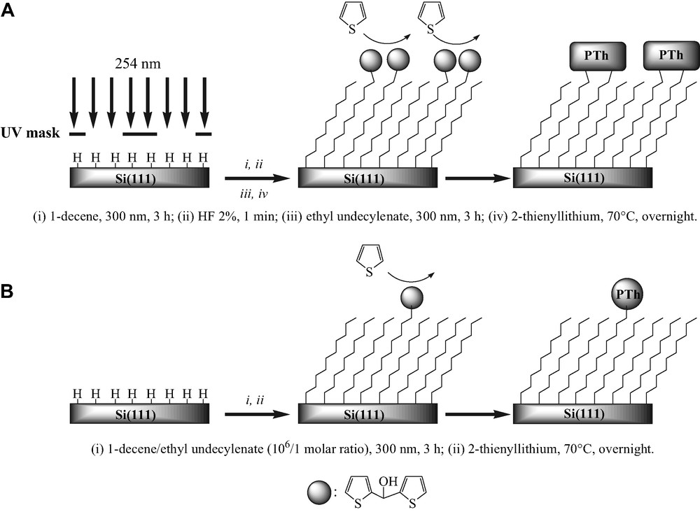
Strategies used for the (A) micro- and (B) nanopatterning of polythiophene (PTh) films chemically bound to silicon (see the text for details).
2.2 Preparation of polythiophene nanopatterns covalently bound to silicon
A Si(111)–H surface was transferred under argon into a mixture of pure 1-decene and ethyl undecylenate present at very low concentration (molar ratio of 10–6). The irradiation at 300 nm for 3 h led to the covalent attachment of the mixed monolayers. The modified silicon substrate was then rinsed and reacted with 2-thienyllithium, as detailed above. Polythiophene nanopatterns were photoelectrogenerated from this surface by potential cycling between –0.5 and 0.85 V at 0.02 V s–1 over a single scan in the same electrolytic solution than previously (Fig. 1B).
2.3 Electrochemical instrumentation
The cyclic voltammetry experiments were performed with an Autolab electrochemical analyzer (PGSTAT 30 potentiostat/galvanostat from Eco Chemie B.V., equipped with the GPES/FRA software) in a self-designed three-electrode Teflon cell. The working electrode, modified Si(111) (area ~0.68 cm2), was pressed against an opening in the cell bottom using an O-ring seal. An ohmic contact was made on the previously polished rear side of the sample by applying a drop of an In-Ga eutectic (Alfa-Aesar, 99.99%). The counter electrode was a platinum foil and all potentials were relative to the system 10–2 M Ag+/Ag in acetonitrile (+0.29 V vs. aqueous SCE).
Tetra-n-butylammonium perchlorate Bu4NClO4 was purchased from Fluka (puriss, electrochemical grade). Acetonitrile (Merck) was freshly distilled over calcium hydride prior to use. The electrolytic medium was dried over activated, neutral alumina (Aldrich) for 30 min, under stirring and under argon. About 30 ml of this solution was transferred with a syringe into the electrochemical cell. The samples were illuminated by an optical fiber from Fiber Lite (Model 190). All electrochemical measurements were carried out inside a home-made Faraday cage, at room temperature (20 ± 2 °C) and under a constant flow of argon.
2.4 AFM
AFM images were recorded with a Nanoscope IIIa from Digital Instruments using silicon nitride (contact-mode) sharpened tips. They were taken in ambient air and flattened. The images were processed with WS × M 3.0 Beta 2.3 Scanning Probe Microscopy free of charge software available from Nanotec Electronica S.L.
3 Results and discussion
The strategy used for the micropatterning of polythiophene films chemically bound to silicon is summarized in Fig. 1A. It is based on the selective electrodeposition of polythiophene on silicon modified with a thiophene-terminated monolayer, previously patterned by UV photolithography [17]. The photoelectrochemical oxidation of this patterned surface in the presence of thiophene leads to polythiophene squares and disks with lateral dimensions in the range of 10–100 μm and thicknesses of some to tens of nanometers (Fig. 2). Under these conditions, the terminal thienyl units inside the patterns are used as the anchoring sites for thiophene polymerization.
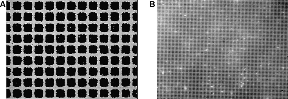
CCD optical images of (a) 80 nm thick ClO4–-doped polythiophene 100 μm squares and (b) 15 nm thick ClO4–-doped polythiophene 10 μm squares covalently bound to n-doped Si(111). The areas surrounding the squares are the decyl regions. The experimental conditions for the formation of these polythiophene arrays are indicated in the experimental part.
Furthermore, the electronically conducting character of the electrogenerated microstructures could be evidenced by recording the Kelvin probe force microscopy image simultaneously with the topography image [17].
In order to evaluate the electrical characteristics of the micropatterned hybrid junctions, the as grown perchlorate-doped polythiophene microstructures are chemically reduced using triethylamine and subsequently doped with gold tetrachloride using a procedure developed by Abdou and Holdcroft [18,19]. This treatment is found to improve the stability of the polythiophene conductivity. The conductivity of the gold tetrachloride doped films is in the range of 20–100 S cm–1 depending on the film thickness and is stable over several weeks under ambient conditions. A typical current–voltage curve through a single tetrachloride gold doped polythiophene/decyl/silicon junction is shown in Fig. 3. The expected diode behavior is clearly observed and the rectification factor measured at +1 and –1 V is around 1000. From the temperature dependence of the current–voltage curves, some other characteristic diode parameters have been determined [20]. Among them, the diode ideality factor is estimated at 2.4. The nonideal behavior of these junctions can be attributed to the discontinuous nature of the organic/inorganic interface [21].
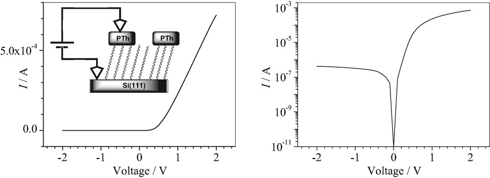
Current–voltage curves in the linear and logarithmic forms through a single 100 × 100 μm2 square of 80-nm-thick AuCl4–-doped polythiophene/decyl/n-Si(111) junction (as in Fig. 2a).
Then, we have wished to prepare polythiophene nanopatterns, using silicon surfaces modified with two mixed organic monolayers (Fig. 1B). This relatively simple synthetic method involves the high dilution of the thiophene-terminated monolayer with an inert decyl monolayer. Thus, the molar ratio between decene and ethyl undecylenate is deliberately fixed at 106 in order to have a long distance between the terminal dithienyl carbinol moieties enough to avoid the connection by the conducting polymer of two neighbour nuclei. Moreover, a short polymerization time (i.e. some seconds) is required to limit the propagation of the electropolymerization process over the surrounding decyl modified silicon areas. If ones assumes that the thiophene-terminated chains are distributed randomly into the matrix of the decyl chains and the surface composition of the two monolayers is not too different from that of alkenes in solution, it is expected that one electropolymerizable moiety will be embedded in a 500 nm decyl square considering an interchain distance of 5 Å [2,22]. Accordingly, the surface would contain four thiophene-terminated chains per square micrometers. A typical AFM image of the mixed monolayers attached to silicon is shown in Fig. 4. The terraces of Si(111) are clearly visible and the surface is defect-free atomically flat with a rms roughness of 1.2–1.3 Å.
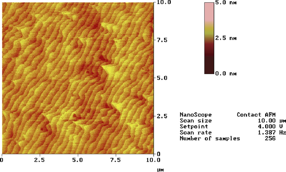
Contact-mode (10 × 10 μm2) AFM image of two mixed dithienyl carbinol-terminated decyl and decyl monolayers covalently bound to n-Si(111).
After the thiophene photoelectropolymerization, the surface topography is characterized by the presence of numerous nanoscale spots, the density of which is in the range of 6–20 μm–2 depending on the scanned areas of the surface (Figs. 5 and 6). Moreover, the spot size is found to vary from 25 to 60 nm. As already reported for the electrogenerated micropatterns, the conducting character of the spots can be also evidenced by recording the Kelvin probe force microscopy image [23].
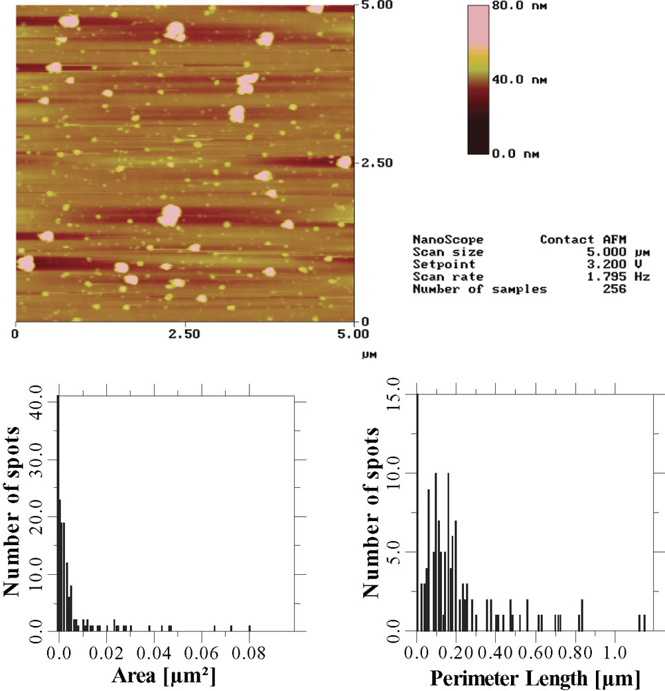
Contact-mode (5 × 5 μm2) AFM image of polythiophene nanopatterns photoelectrogenerated from the two mixed dithienyl carbinol-terminated decyl and decyl monolayers covalently bound to n-Si(111) in the presence of thiophene (see Section 2). The number of spots and the nearest-neighbor distance have been estimated at 157 (i.e. 6.3 μm–2) and 231 nm respectively.

Contact-mode (2 × 2 μm2) AFM image of other polythiophene nanopatterns photoelectrogenerated from the two mixed dithienyl carbinol-terminated decyl and decyl monolayers covalently bound to n-Si(111) in the presence of thiophene (see Section 2). The number of spots and the average nearest-neighbor distance have been estimated at 83 (i.e. ~20 μm–2) and 120 nm respectively.
Globally, the processing of AFM images shows that both the spot density and the nearest-neighbor distance are larger and smaller, respectively, than those predicted from the molar ratio of the precursor alkenes. That would indicate that the surface coverage of thiophene-terminated alkyl chains is likely larger than expected. This result can be ascribed to the reaction of thienyllithium with some hydrogen-terminated silicon areas remaining after the attachment of the two ester-terminated and decyl monolayers [4]. It must be noted that the analysis of the modified silicon surface by high-resolution electron energy loss spectroscopy (HREELS) and XPS does not indicate the presence of sulfur.
4 Conclusions
In conclusion, we have prepared micro- and nanopatterned conducting polymer/silicon hybrid junctions with covalent linkages at both bottom and top contacts.
It should be possible to tune the electrical properties of these diode structures using a conducting polymer as the top contact either by changing the conductivity of the organic material (by electrochemistry for example), the length of the insulating alkyl chain or the dopant type or the density of the semiconductor. Finally, we are currently investigating the nanopatterning of polythiophene on silicon using an electropolymerization reaction initiated by the conducting AFM tip.