

 CC-BY 4.0
1. Introduction
The issue of environmental remediation is one of the most discussed modern challenges. The economic activities of developed and developing countries have important impacts on water and air quality [1, 2, 3, 4]. Industrial activities are clearly the largest source of pollution; therefore, the challenge for the 21st century is the control of technological processes in all industries to develop atom-economical and environment-friendly processes without by-products [5, 6, 7, 8]. However, organic waste such as that from sewage or farming activities also have an important environmental impact. Every day, 2 million tonnes of sewage and industrial and agricultural waste are discharged into the world’s water (UN WWAP 2003), the equivalent of the weight of the entire human population of 6.8 billion people. This is critical, knowing that only 2.5% of the total volume of available water on Earth is fresh. What is more, according to WHO and UNICEF, approximately 894 million people globally do not have access to improved water sources. On average, 250 million people worldwide succumb to diseases related to water pollution annually [9].
Water purification in modern societies has become a critical need. In general, water purification consists of complex physicochemical processes such as coagulation and flocculation into an insoluble phase, sedimentation, several filtration steps, and disinfection [10, 11, 12]. Several types of disinfection exist, such as the use of chlorine, ozone, or UV radiation. However, the purified water introduced into the rivers still contain chemical substances such as antibiotics or pesticides. This means there is a need to improve the efficiency of water purification to increase the accessibility of purified water and to prevent the release of pollutants into the ecosystem [13].
The photocatalytic approach was proposed several decades ago as an ecofriendly solution for water and air remediation by the degradation of pollutants in the aqueous or gas phases [1, 2, 10, 14].
The possibility of the degradation of complex organic compounds into simple CO2 and H2O seems very attractive and promising for environmental remediation. A range of semiconductor materials can initiate the redox degradation mechanism due to their electronic band structures. The first water-splitting property was shown by Honda–Fujishima on titanium dioxide, initiated by the irradiation lower than 400 nm that corresponds to the TiO2 band gap at 3.0 eV [15]. Since then, a large number of investigations have been published over the last four decades. However, the high potential of this approach still attracts interest from the scientific community.
The existing photocatalytic materials that meet the criteria, namely, chemical stability, biocompatibility, nontoxicity, and low cost, are TiO2, ZnO, and SnO2 [16, 17].
The main problem of basic photocatalysis is the wide band gap that limits the light absorption. In fact, the activation of photocatalytic materials is only allowed for light with lower wavelengths (higher frequencies) than the band gap energy; this means that only 3–4% of the solar spectrum could be involved in the photocatalytic reaction. Activation of the photocatalytic material under visible light became a major challenge for the scientific community. However, it is not only the limited range of light frequencies but also a short carrier lifetime due to recombination that reduces its efficiency.
2. Principle of photocatalysis
A catalyst is a substance that allows the acceleration of a chemical reaction by lowering its free activation energy while the catalyst itself does not undergo any permanent modification [18]. A photocatalyst is a photosensitive substance that manifests its catalytic properties via a photon absorption. One can draw a simplistic analogy with photosynthesis in green plants in which chlorophyll plays the role of a photosensitive catalyst to transform CO2 and water into energy and O2 (Figure 1). A photocatalyst is typically a semiconductor material that under light irradiation and in the presence of water and/or oxygen forms a highly reactive species, i.e., radicals. These radicals have a strong ability to oxidize organic molecules and enable their degradation.
Simplistic comparison between photosynthesis and photocatalysis [18].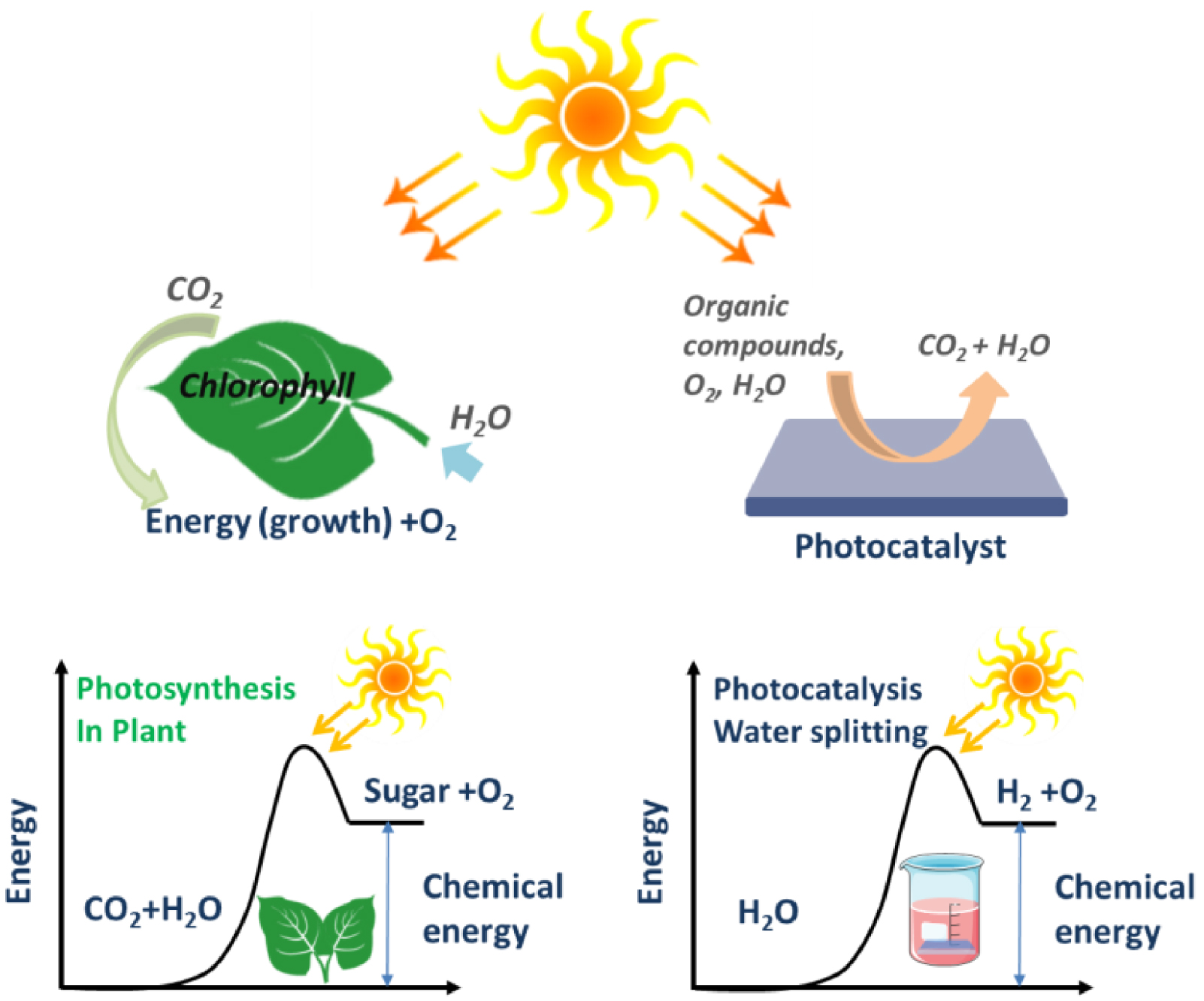
Since Honda–Fujishima [15] first reported on water splitting into O2 and H2 under UV irradiation at 400 nm on titanium dioxide electrode, the domain of photocatalysis has undergone significant development. Various photocatalytic materials have already been reported in the literature. They are classified among the families of metal oxides, metal sulfides, metal nitrides, as well as metal free compounds such as polymers or graphene [19, 20]. Metal oxides such as TiO2, ZnO, Fe2O3, ZrO2, SnO2, MgO, GeO2, Sb2O3, V2O5, WO3, In2O3, and Nb2O5 as well as perovskite materials are among the most investigated materials for photocatalysis today. The particular interest in classically photocatalytic materials such as TiO2 and in a lesser extent ZnO and SnO2 is due to their high photocatalytic activity, good chemical stability, non- or low toxicity, and low cost.
One of the key elements characterizing photocatalytic materials is the interaction with light and, in particular, the photon absorption. A photon with an energy higher than the semiconductor band gap energy can be absorbed by the photocatalytic material. A photon absorption will excite electrons from the valence band (VB) and promote them to the conduction band (CB) , generating holes in the VB . These generated carriers (e−,h+) may migrate to the material surface and since they are in contact with water and/or oxygen molecules, they induce the formation of OH∙ and radicals (Figure 2) [21].
Scheme of the photocatalysis principle [21].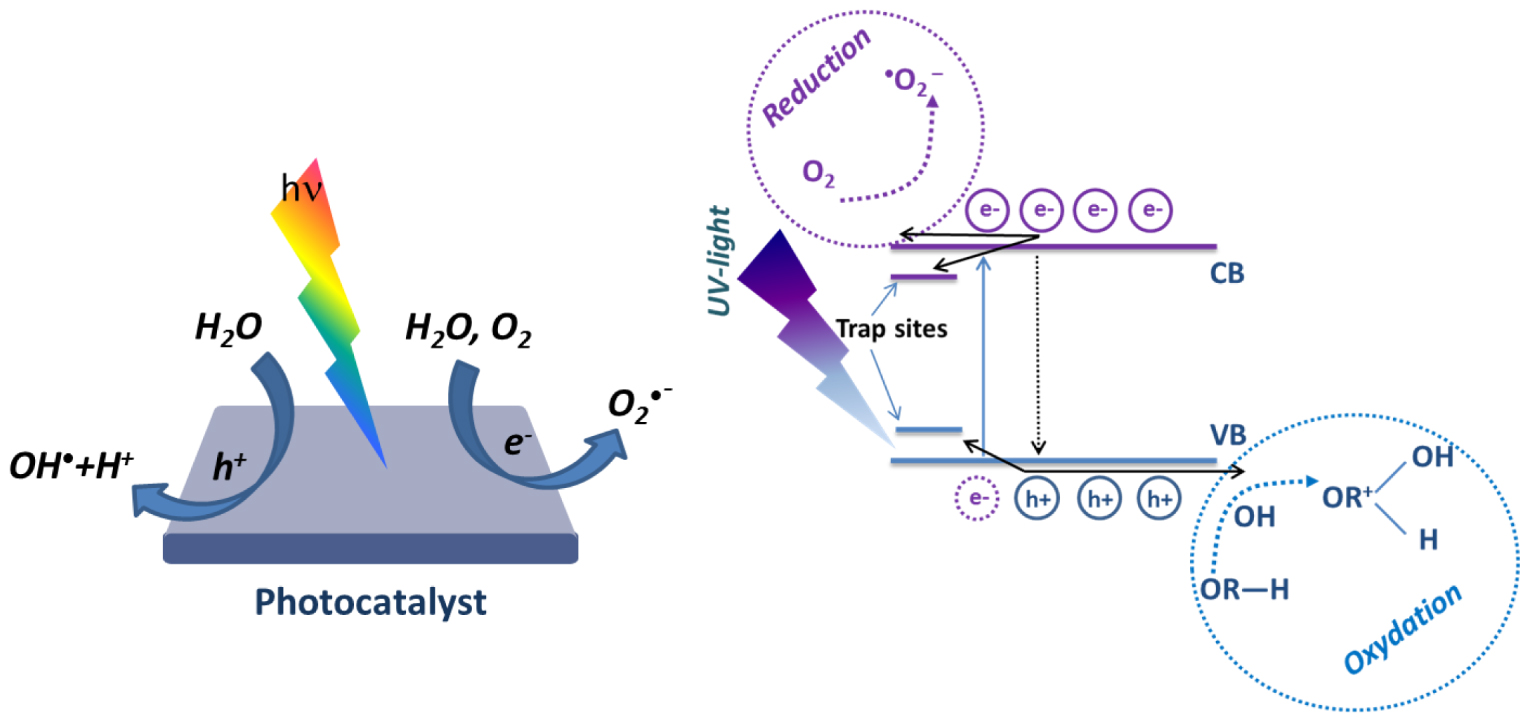
On the surface and depending on the photocatalyst, holes have a typical oxidative potential from + 1 to + 3.5 V compared to the Normal Hydrogen Electrode (NHE), and electrons have a reduction potential from + 0.5 to − 1.5 V [16, 22]. The redox potential value of the semiconductor is determined by its electronic band structure. The main condition of OH∙ radicals generation is that the potential of valence band should be higher than the potential of hydroxyl radical formation.
Band gap energy for TiO2, ZnO, and SnO2 on a potential scale (V) versus the normal hydrogen electrode (NHE) [23].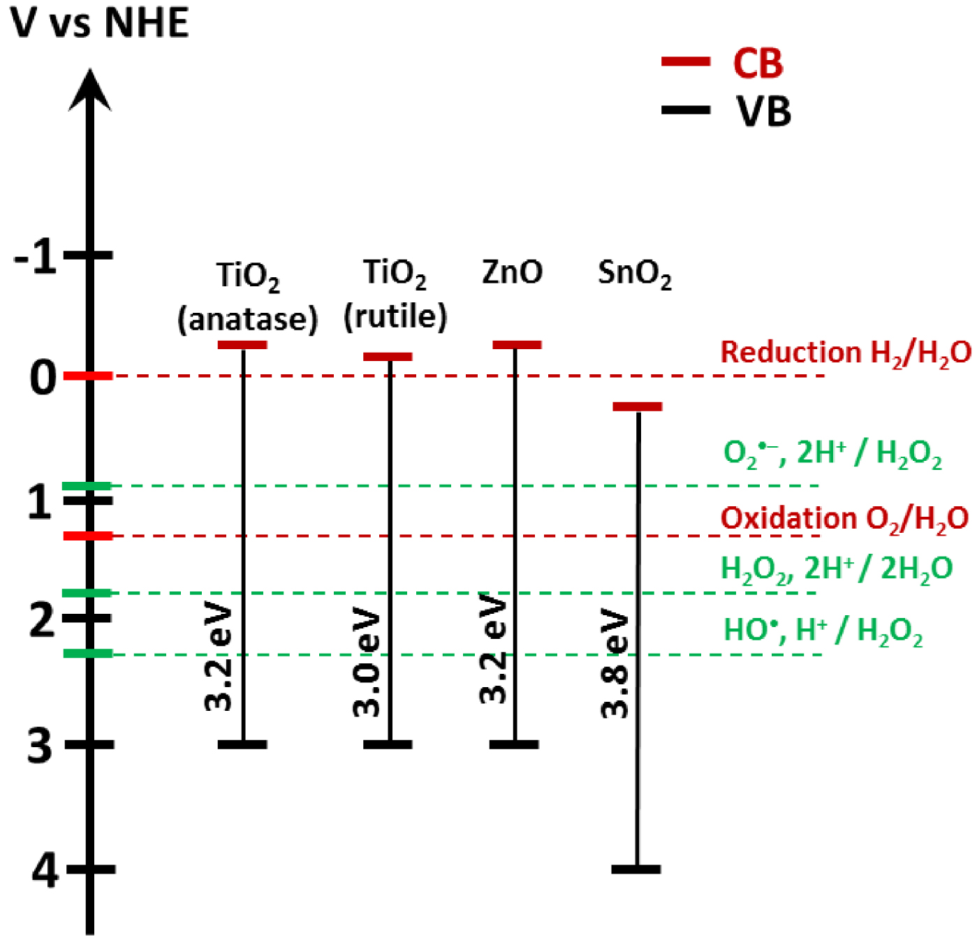
Figure 3 represents the positioning of the band gap energy compared to the potential of radical formation. The redox potential of OH∙, H+∕H2O is 2.31 V vs NHE [23]. The formation of superoxide radicals by requires a potential of 0.92 V vs NHE. Superoxide radical formation is typically induced when the semiconductor’s CB energy is higher than this threshold potential.
In order to fully understand the activity of photocatalysts, the determination of the lifetime and mobility of photogenerated charge carriers must also be carefully studied. In materials like ZnO or TiO2, carriers recombine over the nanosecond period [24]. However, the relaxation time and spatial distribution of carriers are a function of multiple parameters like the chemical environment, the presence of defects in the material or the crystal structure [25]. Thus, spatial and time resolved characterization techniques are mandatory to determine the lifetime and surface availability of carriers. The photogenerated charge carriers’ relaxation time can be studied using time resolved fluorescence spectroscopy, transient absorption spectroscopy [25, 26], or time resolved microwave conductivity [27]. Spatial distribution can be determined by Kelvin probe force microscopy (KPFM) [28], electrostatic force microscopy (EFM) [29], or conductive atomic force microscopy (C-AFM) [30].
The degradation of organic molecules mainly relies on high oxidative potential of OH∙ radicals, which enables the breaking of C–C bonds. A typical photocatalytic degradation reaction of organic molecules has been reported with TiO2 as photocatalyst [21, 22, 31]:
The carriers are photogenerated under photon absorption within a few femtosecond range:
| (1) |
The electrons in contact with the adsorbed oxygen molecules demonstrate their reductive potential and form superoxide radicals:
| (2) |
The interaction between holes and water molecules produces hydroxyl radicals :
| (3) |
The superoxide radicals being very reactive (nonstable), they can react with and undergo a fast transformation in OH∙ radicals:
| (4) |
| (5) |
| (6) |
Hydroxyl radicals enable the organic molecule oxidation:
| (7) |
| (8) |
The determination/quantification of photocatalytic degradation performances of photocatalysts is usually followed through the degradation of kinetic of organic molecules. Many organic molecules can be used as a chemical probe, like salicylic acid, formic acid, phenol, or dyes/azo dyes like methylene blue or methyl orange. For molecule owning aromatic cycles or chromophores, their degradation processes can be easily followed with UV-visible absorption measurements. It is the case for salicylic acid, phenol, methylene blue, and methyl orange. Concerning the degradation of formic acid, it can be tracked by measuring the amount of released during its decomposition.
The photocatalytic degradation of aromatic cycles follows a mechanism starting with the hydroxylation of free sites followed by a rupture of the cycle and its decomposition in smaller molecules. Devi et al. [32] evidenced this mechanism, based on the phenol molecule, as presented in Figure 4. Phenol mineralization involves first a hydroxylation step leading to dihydroxybenzene (catechol, resorcinol or hydroquinone), followed by the cycle opening forming pent 2-enedioic acid or benzoquinone both leading to maleic acid. As the process progresses, the maleic acid dissociates in oxalic acid and finally mineralize in CO2 and H2O.
Experimentally, the intensity of the absorption peak corresponding to the aromatic cycle of the molecule lowers as the photocatalytic degradation process progresses.
Photocatalytic degradation pathway of phenol. Reproduced from [33].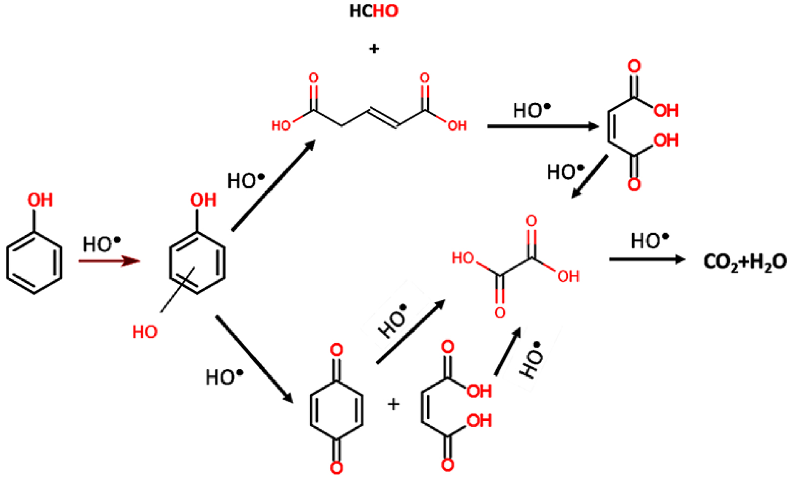
Photocatalytic degradation experiences based on the decolorization of organic dyes are also commonly found in the literature [34]. In such processes, the decolorization of the molecule is due to the destruction of chromophoric groups of dyes. Consequently, the decolorization of water can be monitor by visible absorption, but it does not certify the complete mineralization into CO2 and H2O. It is possible that some by-products form in the water, with sometime a higher degree of toxicity than the primary molecule [35]. Thus, the UV-visible absorbance characterization is a strong technique to follow the disappearance of an absorbing group, but it does not give any confirmation of the mineralization. Other techniques like LC–MS [36] or Total Organic Carbon (TOC) measurement [37] can thus be complementary.
Crystalline structures of anatase, rutile, and brookite phases.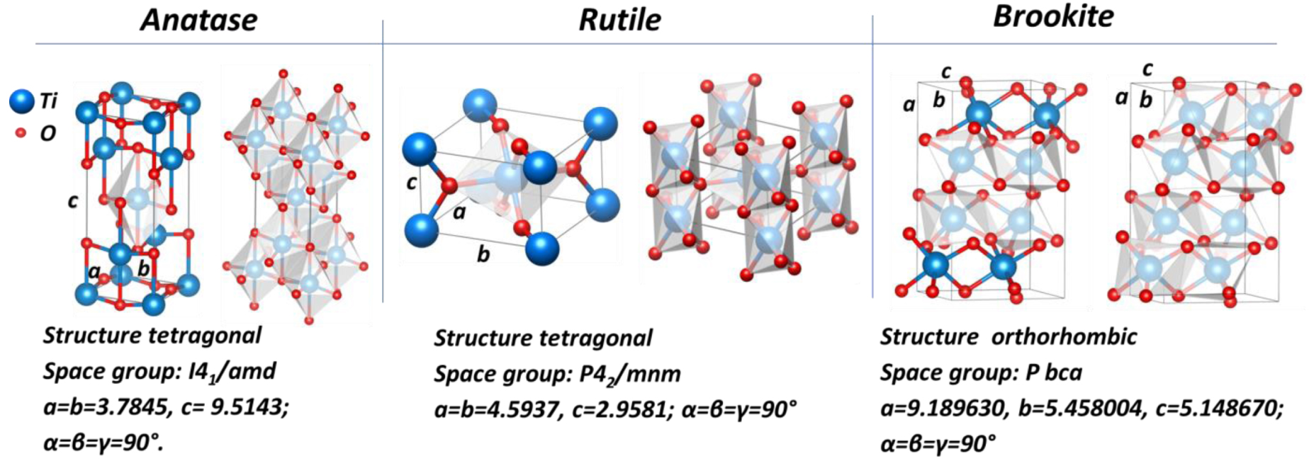
3. Basic photocatalytic systems
Typically, photocatalytic systems belong to the family of binary metal oxides such as TiO2, ZnO, or SnO2. These materials can be characterized as wide band gap semiconductors having a light absorption in the UV range. Historically, TiO2 (particularly TiO2 Degussa Evonik P25) was the first commercialized and mainly used material for its photocatalytic properties. Tin oxide, having particular electronic and optical properties, is also successfully applied in photocatalytic degradation, but requires deeper UV irradiation [31].
3.1. Titanium dioxide (TiO2)
Improvement of the photocatalytic degradation process requires a clear understanding of photocatalytic material properties. Although TiO2 is the most studied photocatalyst, it continues to attract attention from the scientific community. The various TiO2 applications are principally based on UV-light absorption, such as UV-light protection, photocatalysis, hydrogen production, and solar cells. TiO2 is also applied in gas sensors, varistors, and as anti-corrosive coatings.
Summary of anatase and rutile physical properties [38]
| Anatase | Rutile | ||
|---|---|---|---|
| Lattice parameter | |||
| a (Å) | 3.7874 | 4.5937 | |
| c (Å) | 9.5147 | 2.9587 | |
| Density (g∕cm3) | 3.894 | 4.250 | |
| TiO6 coordination number | 8 | 10 | |
| Dielectric constant | |||
| ⊥ | 31 | 89 | |
| ∥ | 48 | 173 | |
| Electron effective mass | 1m0 | 9–13m0 | |
| Hall mobility (cm2∕V⋅s) | 15–550 (crystal) | 0.1–10 (crystal) | |
| (300–10 K) | 4 (thin film) | 0.1 (thin film) | |
| Nonmetal–metal transition by a shallow donor band | Yes | No | |
| Excitons | Self-trapped | Free | |
| Luminescence | Visible broad band cantered at 2.3 eV | Sharp peak at 3.031 eV | |
| Optical absorption edge: Eg (eV) | |||
| ⊥ (direct) | 3.420 | 3.035 | |
| ∥ (indirect) | 3.460 | 3.051 | |
3.1.1. Crystallographic structure
TiO2 exists in three main crystallographic phases: anatase, rutile, and brookite. Rutile is the thermodynamically stable phase while anatase and brookite are metastable (Table 1). Both anatase and rutile modifications have tetragonal structures; brookite possesses an orthorhombic structure. For all polymorphic TiO2 structures, TiO6 octahedrons represent basic blocks, where the Ti atom is bonded with 6 oxygen atoms, and each oxygen atom is bonded with three Ti atoms. In the anatase structure, each TiO6 octahedron has 4 shared edges and 4 shared corners with 8 neighbors. The edge shared octahedra are aligned along [100] or [010] direction, forming zigzag chains perpendicular to c axis. In the rutile structure, each TiO6 octahedron is connected with 10 neighbor octahedrons having 2 shared edges and 8 shared corners. The edge shared octahedrons are aligned along the [001] direction. The unit cell parameters for anatase, rutile, and brookite is illustrated in Figure 5.
3.1.2. Electronic properties
TiO2 is a wide band gap semiconductor with a band gap value of 3.2 eV for anatase phase and 3 eV for rutile phase. The anatase phase has a higher electron mobility than the rutile phase due to the lower electron effective mass (1m0 for anatase and 9–13m0 for rutile).
Schematic illustration of possible recombination processes of photogenerated electrons and holes in (a) anatase (indirect gap) and (b) rutile (direct gap) phases [39].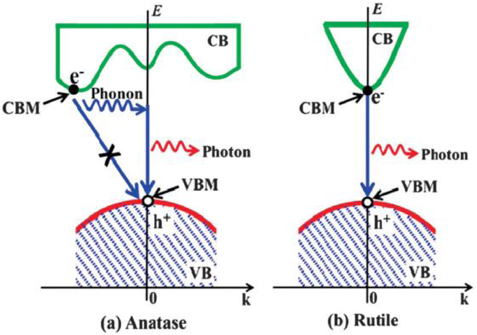
In the TiO2 electronic band gap structure, the maximum of the VB principally gets the contribution of O 2p orbitals and the CB minimum is mainly due to Ti 3d orbitals. It is generally reported that anatase has an indirect, and rutile a direct electronic band gap. However, numerous studies on this topic are still controversial regarding the electronic structure of the band gap. The experimental (spectroscopic) methods of band gap measurements indicate for anatase and rutile phases that there is a dependence of the band gap nature on the electric field orientation. If the electric field is perpendicular to c axis (E ⊥ c), the optical band gap is found to be direct, and indirect if the applied electrical field is parallel to c axis (E ∥ c). Another opinion is about the crystallites size dependency on direct–indirect band gap transition. It was shown by Reddy et al. [40] that anatase nanoparticles with grain size of 5–10 nm exhibit a direct band gap transition. The photocatalytic activity of anatase is known to be more important than for rutile, even despite of the wider band gap [41, 39]. The investigation realized by Zhang et al. [39] demonstrates that in anatase, thanks to the indirect band gap, the lifetime of photogenerated carriers is increased due to the phonons assisted recombination (Figure 6).
Concerning the brookite phase, being less investigated, the literature overview gives contradictory information about the band gap energy. According to the theoretical predictions and reported experimental measurements, the brookite band gap values vary in the range between 3.1 and 3.4 eV [42]. This lack of information could be justified by the difficulty to obtain pure brookite phase. However, the recent advances on hydrothermal synthesis of pure brookite nanostructures raise the interest in this phase, but the film deposition of pure brookite phase remains an open challenge.
It is worth noticing that TiO2 anatase demonstrates a different photocatalytic activity as a function of the dominant crystallographic orientation. It was found that among crystallographic orientations, the facet (001) is the most reactive (Figure 7). This is under intense investigation.
Illustration of anatase crystal facets: (a) Normal anatase crystal; (b) Elongated anatase crystal.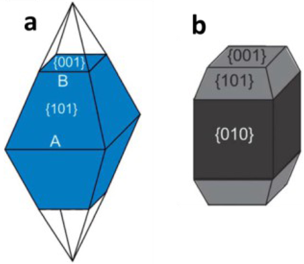
However, being the most energetic facet, it is difficult to obtain, mostly due to the principle of the minimization surface energy during a growth process. The anatase synthesized by conventional methods like CVD or hydrothermal synthesis, contains more than 94% of thermodynamically stable and low-surface-energy (101) facets (Figure 6a). The average surface energy (𝛾) given by theoretical predictions for principal TiO2 anatase facets are: 𝛾 (001) 0.90 J⋅m−2 >𝛾 (100) 0.53 J⋅m−2 >𝛾 (101) 0.44 J⋅m−2 [43]. Currently, hydrothermal synthesis is the most appropriated method to obtain a significant percentage of (001) facets using a shape controlling agent, mainly HF [44].
The thin film deposit ion of (001) facets could be achieved by epitaxial growth on Si (001) substrate with buffer layer SrTiO3∕TiN or on SrTiO3(100) single crystal. It is worth mentioning that the development of new methods tailoring the crystalline orientations and its stability is one of the emerging routes in the research on TiO2. Therefore the crystalline structure of TiO2 and thus potential tailoring of the surface energy has to be taken under consideration as a potential way of enhancing the photocatalytic activity. Nevertheless, the photocatalytic activity remains in the UV range.
3.2. Zinc oxide (ZnO)
After TiO2, ZnO is the second most studied photocatalyst for photocatalytic water/air treatment. It possess properties close to that of TiO2 in terms of light absorption and photocatalytic activity, but its peculiar optical and piezoelectric abilities makes it also suitable for optoelectronic applications like light emitting diodes [45] or piezoelectric material [46]. In addition, ZnO is a cheap and nonhazardous material, easily synthesized with multiple liquid or gas phase processes.
3.2.1. Crystallographic structure
Like many binary semiconductors based on II–VI groups elements, ZnO can crystalize under the form of hexagonal of cubic structures. Most often, ZnO crystalize in the hexagonal wurtzite structure (B4 group), but in some particular cases, it can also exist as cubic zinc blend (B2 group) and cubic rock salt (B1 group) [47]. A schematic illustration of those tree cell structures is presented in Figure 8.
Schematic representation of cell structures for the three different crystallographic phases of ZnO: (a) Rocksalt, (b) Zinc blend, and (c) Wurtzite.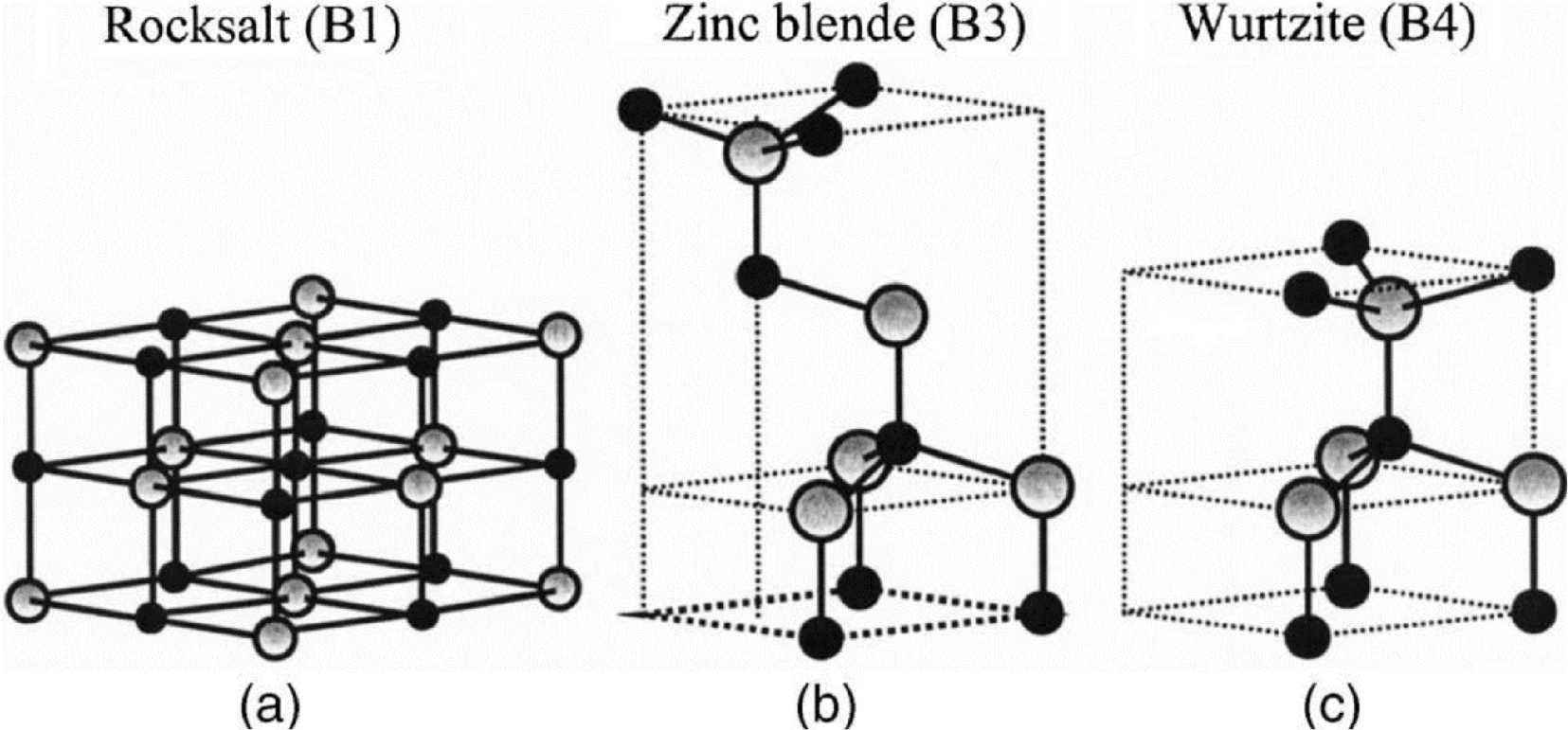
The zinc blend structure can be obtained using a ZnO epitaxial growth on cubic structured substrates whereas the rock salt one can only be synthesized under high temperature and pressure (around 9 GPa) conditions [48]. For those reasons, almost all ZnO-based materials found in the literature are hexagonal wurtzite. The wurtzite structure belongs the P63mc space group according to the Hermann–Mauguin classification, and group according the Shoenflies one. ZnO hexagonal wurtzite lattice parameters are a = b = 3.250 Å and c = 5.206 Å, with 𝛼 =𝛽= 90°, 𝛾 = 120° (JCPDS 79-2205).
Electronic band structure of ZnO calculated by DFT. Reproduced from [49].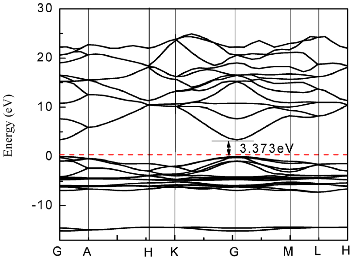
3.2.2. Electronic properties
ZnO is a semiconductor with a direct band gap of 3.2–3.4 eV. Density Functional Theory (DFT) calculations used for the determination of bands structures for the ZnO wurtzite crystal are presented in Figure 9. They reveal that the maximum of the valence band and a minimum of the conduction band are located at the symmetry point G. In addition, the valence band maximum is at the energy zero point (Fermi level). It highlights the direct electronic band gap, with a band gap calculated here at 3.373 eV [49].
SnO2 cassiterite unit cell.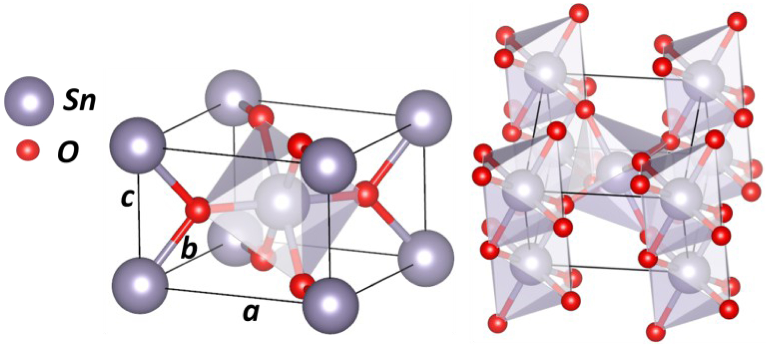
With a band gap of 3.2 eV, ZnO absorbs light in the UV-A range of the light spectrum and show photoluminescent emission properties around 380 nm corresponding to the excitonic radiative recombination. Local Density Approximation (LDA) calculations reveal that the maximum of the valence band principally get the contribution from oxygen 2p orbitals, whereas the minimum of the conduction band principally get contribution from zinc 4s orbitals [50].
3.3. Tin oxide (SnO2)
Tin oxide is another wide band gap semiconductor which is already used in numerous fields like transparent electrodes, gas sensors etc [51, 52, 53]. The combination of optical transparency and high conductivity makes SnO2 very attractive for optoelectronic, photocatalytic and photovoltaic applications.
The electronic band gap structure of Tin oxide [54].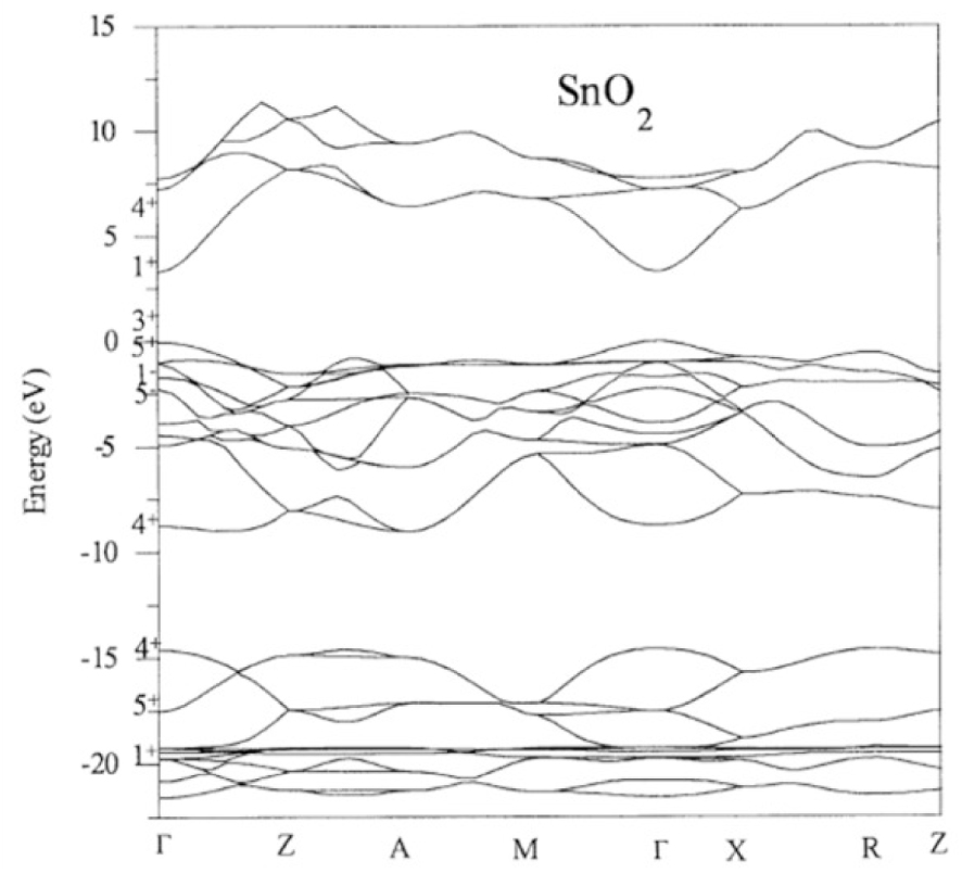
3.3.1. Crystallographic structure
SnO2—cassiterite (or rutile phase) has a tetragonal crystallographic structure with space group P42/mnm and lattice parameters a = b = 4.731 Å and c = 3.189 Å. A schematic illustration of the cassiterite unit cell is represented on Figure 10. Cassiterite’s crystallographic parameters are very close to TiO2 rutile. As with the TiO2 rutile structure, SnO2 has SnO6 octahedron building blocks, were each cation (Sn) is connected to 6 anions (oxygen).
3.3.2. Electronic properties
Tin oxide has a direct band gap with an energy value between 3.6 and 3.8 eV and an n-type conductivity [55]. The electronic band gap structure along high symmetry directions is represented on Figure 11.
In the SnO2 electronic bands structure the maximum of the valence band (VB) principally get the contribution from oxygen 2p orbitals while the minimum of conduction band (CB) is mainly due to tin 4s orbitals. Tin oxide shows a possibility to change a stoichiometry on the surface and become SnO, where Sn4+ can be reduced to Sn2+. This modification has an important effect on the surface electronic structure, leading to the formation of Sn 5s derived surface states, and reduces the work function of the materials. This property is largely used in gas-sensitive applications.
3.4. Limitations of basic photocatalytic systems and solutions
The three main metal oxides TiO2, ZnO and SnO2 are fundamental in the photocatalytic approach. However, their electronic and optical properties have few important drawbacks that limit its photocatalytic potential. The wide band gap of metal-oxide semiconductors represents the first important limitation. The light absorption allowed only for photons with higher energy than the respective band gap energy restricts the use of classical photocatalysts in the UV range of sun light. It means that only 3% of the solar spectrum is involved in a photocatalytic degradation reaction. Therefore, one of the current challenges is to push forward the light absorption to the visible range.
The second issue is the low stability of the photogenerated carriers; in particular, their fast recombination (few nanoseconds) represents one of main issues in photocatalysis. This phenomenon could be avoided by the addition of electron and hole scavengers, which could be various metastable surface states, electron donors or electron acceptors adsorbed on the semiconductor’s surface [16]. Consequently, the increase of photocatalytic system efficiencies could be reached by acting principally on the band gap structure, in order to increase the range of absorption and reduce the carrier recombination.
3.5. Doping
In the semiconductor industry, doping is one of the main approaches to tune the Fermi level. In photocatalysts, the doping approach consists of a direct modification of the band gap structure by creating additional energetic levels, in order to extend the light absorption and also create trap sites of carriers to prevent the fast recombination [56]; n-type doping of TiO2 by C, N, P, S, B has shown a significant improvement of the visible range light absorption in the photocatalytic material. The nitrogen incorporation within TiO2 lattice has demonstrated the photocatalytic activity in the visible range that opened a potential way for the improvement of photocatalytic systems. The visible range absorption may be induced by the substitutional or interstitial nitrogen incorporation. The impurity incorporation in the metal-oxide lattice may create oxygen vacancies which may also be responsible of the photocatalytic efficiency enhancement [57, 58]. The theoretical prediction through DFT calculations showed that, in the case of substitutional N-doping, the occupied N 2p localized states are slightly above the valence band edge (Figure 12). While for the interstitial incorporation of nitrogen, the unpaired electron is shared between the N and O atoms and formed NO bond. That generates π-type localized states which are higher than the valence band edge of 0.73 eV [57, 59].
Schematic of possible N-doped TiO2 crystalline structure [57, 59].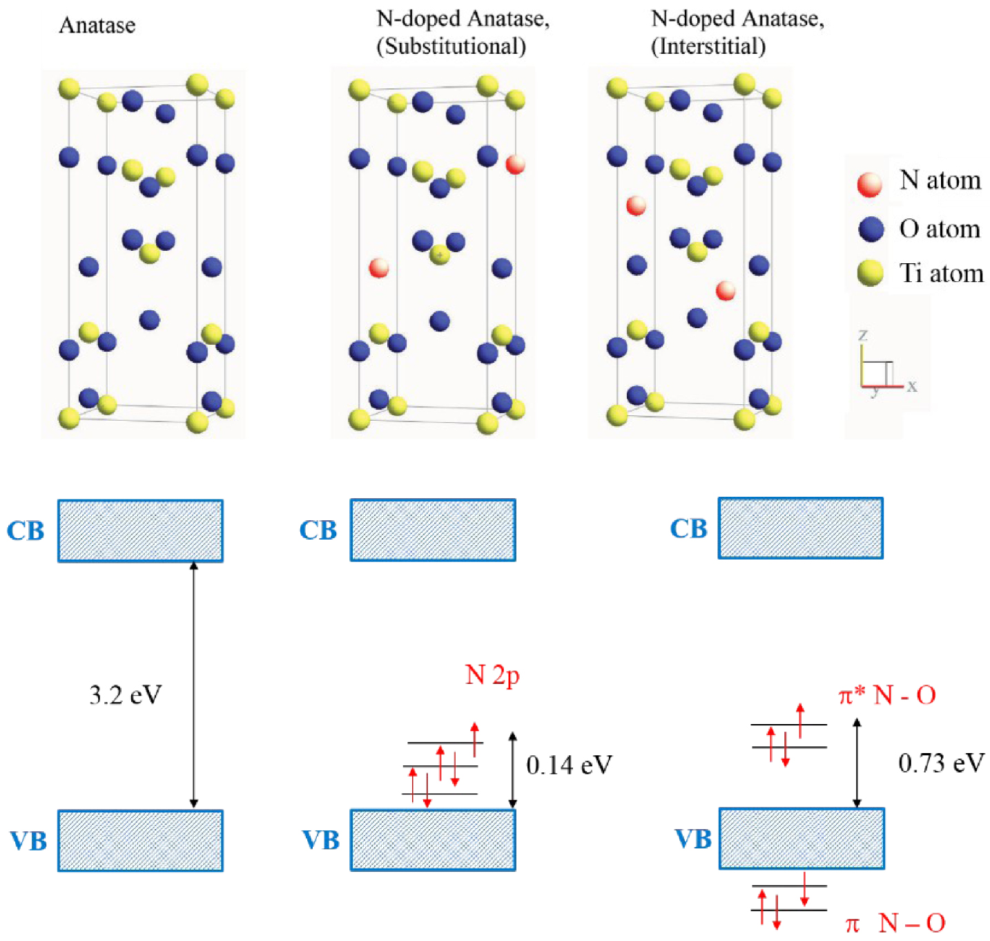
Besides the N-doped TiO2, doping with Boron- Carbon- and Fluorine are extensively studied in the literature and appear as also attractive candidates for the significant improvement of the photocatalytic activity [58, 60]. However the bang gap tailoring through the impurity incorporation in the metal-oxide lattice may also have a reverse effect and promote the undesirable fast recombination of carriers.
3.6. Stoichiometry
Oxygen vacancies (VO) are particular defects of the crystalline lattice, which could be present either in bulk or on the surface and results in reducing of Ti4+ to Ti3+ [58]. The presence of Ti3+ defects, also called a self-doping significantly enhance the light absorption of TiO2 in the visible range creating the inter-band gap states. Therefore, the attention to nonstoichiometric TiO2 has been increased recent years [61, 62, 63, 64]. The oxygen vacancies in the TiO2 lattice can be created by the high vacuum annealing or the use of a reduction agent. However, the important drawbacks of these methods are high cost and critical experimental conditions. Last years an important number of publications report on the hydrothermal approach offering better control on the Ti3+ generation [61, 63, 64, 65]. The Ti3+ self-doped TiO2 powder synthesized by the hydrothermal approach confirms the significant enhancement of TiO2 photocatalytic performances in the visible range. Sasinska and co-workers [66] achieved a highly Ti3+ doped film by realizing the hydrogen plasma post-treatment of amorphous TiO2 films deposited by ALD [66]. The H2 modified TiO2 films demonstrated significant improvement of the photocurrent density and the light absorption in the visible range.
3.7. Heterostructures
The fabrication of heterostructures does not imply the band gap modification of each material participating in the heterostructure as in the doping approach. Instead, it involves the combination of materials with different band gap energy levels and the formation of heterojunction.
As mentioned previously, to prevent the fast recombination of photogenerated electrons and holes, they have to be separated. The band gap engineering via the heterostructure fabrication acts principally to improve the carrier’s separation and thus increases their lifetime, and consequently the photocatalytic efficiency. When the semiconductor interface forms an energy gradient that promotes the carriers’ separation, the staggered gap (SG) is formed, and the electrons will intend to migrate into the semiconductor with the lowest energy position of conduction band (CB1). This is contrary to the holes that would migrate to the semiconductor with the highest position of the valence band (VB2), as shown in Figure 13. The assembly of SnO2 and TiO2 must be noted (Figure 14). XPS analysis can be employed to demonstrate the formation of heterostructures. Another example is the SnO2∕ZnO heterostructures [67, 68, 69], where the valence band and the conduction band offsets (VBO (𝛥Ev), CBO (𝛥Ec)) in the heterostructure was calculated using the following equations [67, 68, 69]:
| (9) |
Ev ZnO to the valence band maximum of bulk ZnO;
ESn 3d to the binding energy of the Sn 3d peak in bulk SnO2;
Ev SnO2 to the valence band maximum in bulk SnO2.
Schematic of the staggered gap. CB1 and VB1 represent the conduction band and the valence band, respectively, of the semiconductor 1. CB2 and VB2 represent the conduction band and the valence band, respectively, of the semiconductor 2.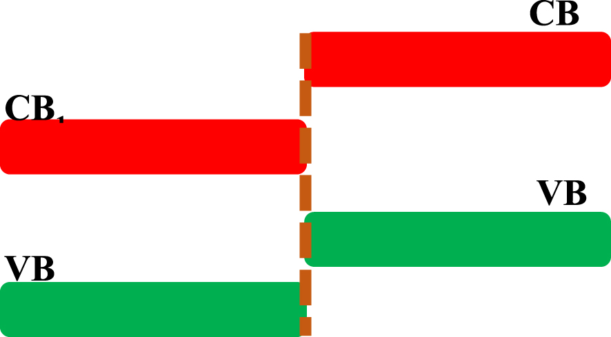
The 𝛥ECL term can be determined from:
| (10) |
The conduction band offset (𝛥Ec) can be calculated by:
| (11) |
The presence of an SG type heterostructure on the ZnO∕SnO2 interface was confirmed with 0.67 eV valence band offset and 0.24 eV conduction band offset on the ZnO∕SnO2 interface [67, 68, 69].
The assembly of various metal-oxide or metal-sulfide semiconductors are known to form a SG type heterostructure. However, ZnO- and TiO2-based heterostructures are still commonly investigated: ZnO∕SnO2 [70, 71, 72, 73], TiO2∕SnO2 [74, 75, 76], TiO2∕ZnO [77, 78, 79, 80], TiO2∕WO3 [81], or ZnO/CuS [82].
Representation of the SG heterostructure present in a SnO˙2∕TiO2 heterostructure.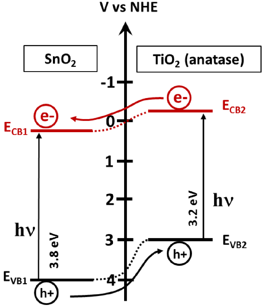
TiO2 and ZnO have very similar electronic properties, such as a band gap value of 3.2 eV, or similar valence and conduction band positions. Tin oxide has a larger band gap value, which limits its absorption to the deep UV range. The assembly of SnO2 with TiO2 or ZnO in heterostructures creates conditions for charge separation and the enhancement of photocatalytic activity; unsurprisingly, they attract considerable attention.
The increased photocatalytic efficiency has been reported in the literature in the case of using Janus type ZnO∕SnO2 and TiO2∕SnO2 heterostructures compared to basic metal-oxide systems. Uddin et al. [71] demonstrated a twice faster rate of photocatalytic degradation of methylene blue (UV at 365 nm–125 W) on SnO2∕ZnO nanoparticles compared to ZnO alone. Similar heterostructure systems show a 100% enhancement on the decolorization of methyl orange solution [72]. The assembly of TiO2∕SnO2 nanoparticles exhibits a 50% increase in the rate of photocatalytic degradation of Rhodamine B compared to commercial TiO2 (Degussa Evonik P25) nanoparticles [76].
A large number of publications discuss the heterostructure assembly of nanowires/nanoparticles, which allows us to draw a conclusion about the efficiency of this approach. The decoration of metal-oxide nanowires grown by various methods with metal-oxide nanoparticles also demonstrates the efficiency of the heterostructure approach [73, 83]. Zhu et al. [83] demonstrated, by photocurrent measurements, that the efficient separation of carriers promotes photocatalytic degradation. As shown, the semiconductor heterostructures can solve the problem of carriers’ recombination; however, the photocatalytic activity will still be limited to the UV range. Moreover, the semiconductor–semiconductor interface should not have any parasitical contamination; otherwise the separation of carriers will not occur.
(a) Schematic illustration of surface plasmon resonance. (b, c) Illustration for plasmon resonance dependency on nanoparticle material and shape [69, 84, 85].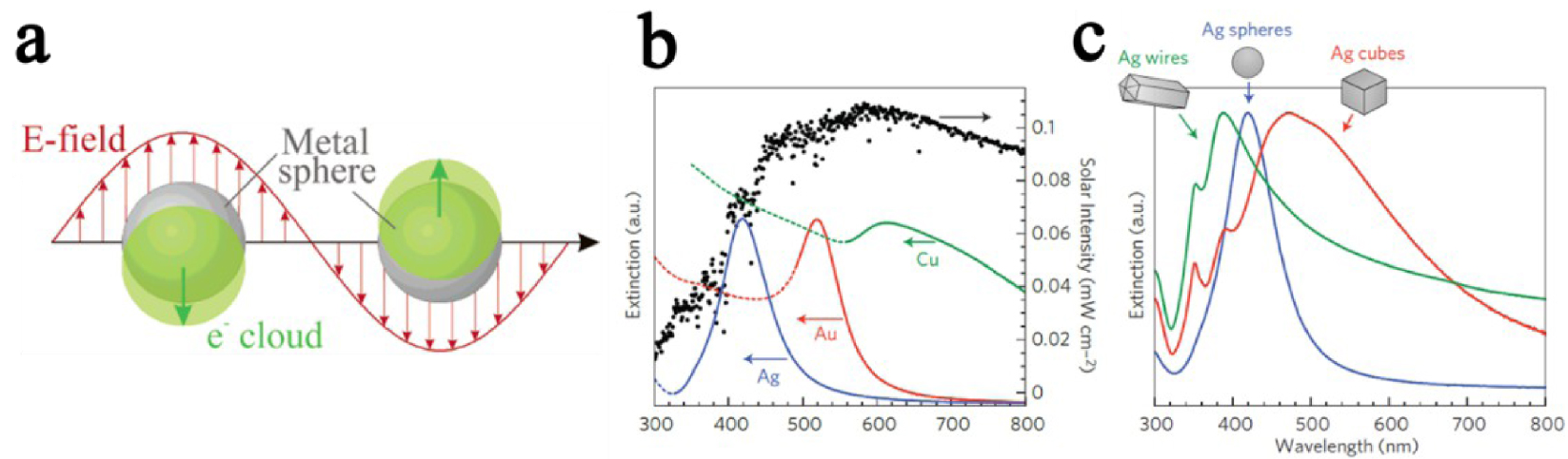
4. Plasmonic approach for the enhancement of the photocatalytic activity
The association of metal-oxide structures with metallic nanoparticles presenting surface plasmon resonance properties is considered as heterostructures as well [86, 87]. Like the process occurring in the case of semiconductor/semiconductor heterostructures, noble metal nanoparticles can trap electrons from the conduction band of a semiconductor. It is due to the Fermi level difference between noble metals and metal oxides. Usually, noble metals possess lower Fermi level than metal oxides, leading to a migration of photogenerated electrons from the conduction band of metal oxides in metallic nanoparticles, through the heterojunction. This process enhances the charge separation and prevents recombination of photogenerated species. In addition, one of the main advantages of plasmonic nanoparticles is that the plasmonic surface resonance appears in the visible range of the light spectrum.
4.1. Principles of the plasmonic approach for improvement of light absorption
Plasmonics address the core idea of a coherent oscillation of electrons in metals induced by the interaction of incident electromagnetic radiation with metallic nanostructures [69]. The principle of this plasmonic surface resonance can be explained by drawing an analogy with a mechanical oscillator [69, 88]. The displacement of a simple harmonic oscillator from equilibrium results in a continuous sinusoidal motion. The amplitude of the harmonic oscillator is a function of the external periodic force frequency applied to the system. When the frequency fulfills the resonance conditions (“in phase” with the system), the amplitude of the harmonic oscillator is increased [69].
Likewise, in plasmonics, an incident electromagnetic radiation (as external force) enhances the oscillation of delocalized electrons from the electron cloud. It induces the emergence of Coulombic forces between the noble metal nucleus and the delocalized electron cloud, opposed to each other. The plasmonic resonance appears when the resultant of those two opposite forces leads to the collective oscillation of the electrons from the electron cloud (delocalized electrons) [69] (Figure 15a).
When metal nanoparticles are smaller than the incident light wavelength, the collective oscillation of electrons is referred to as Localized Surface Plasmon Resonance (LSPR). Multiple parameters affect the oscillation frequency of electrons, such as the effective mass and density of electrons, or the shape, charge distribution, and size of nanoparticles [69, 84, 85]. Among all metals presenting LSPR properties, noble metals are particularly attracting due to their chemical stability, even at the nanometer scale, and their strong LSPR in the visible range of the light spectrum (Figure 15b and c) [69]. Thus, heterostructures between metal-oxide photocatalysts and noble metal nanoparticles showing LSPR properties are particularly appealing for photocatalytic applications, as they are efficient in a broader light spectrum range (especially visible range), and improve photogenerated charge carriers separation [69]. In the UV range, nanoparticles behave as collectors for the incident light, resulting in an improved absorbance of the electromagnetic field at the metal-oxide surface, through an LSPR mechanism. Previous publications, studying the mechanism at the origin of the improvement of photocatalytic properties of metal-oxide/plasmonic nanoparticles, stated the aptitude of nanoparticles to enhance the separation of charge carriers [69]. In the suggested mechanism, the interface between plasmonic nanoparticles and the photocatalytic metal oxide was considered as a Schottky barrier [69, 89, 90, 91, 92, 93, 94]. In the visible range, electrons originating from the oscillating electron cloud in the metallic nanoparticles are injected in the conduction band of the metal oxide (Figure 16) [69]. In the process depicted in Figure 16, electron migration from the gold nanoparticle to the TiO2 leads to a temporary oxidation state of the gold nanoparticle. As stated by Tian and Tatsuma [91], this oxidized state reduces quickly with an electron provided by a donor present in the solution. Femtosecond IR analysis performed by Furube et al. [92] showed that this electron reduction happens within a few hundred femtoseconds [69].
Possible mechanism of charge separation (direct charge transfer mechanism) [91].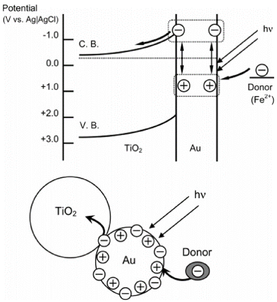
The mechanism behind the global photocatalytic improvement is still not fully understood. However, the direct charge injection is appearing as the most supported one, based on experimental and theoretical studies [69, 95, 96].
Another interesting property of plasmonic nanoparticles is the local heating effect. It originates from the local electromagnetic field produced by the plasmonic resonance. This local heating effect is particularly interesting in applications like photothermal catalysis, medicine, synthesis, or light-to-heat conversion systems [97, 98, 99]. Fasciani et al. [100] highlighted that the local temperature at the surface of gold nanoparticles could attend 500 ± 100 °C under laser pulses (8 ns, 532 nm, 50 mJ/pulse).
In the literature, multiple associations of metal oxides and metallic nanoparticles can be found. Most often, metal oxides are ZnO, TiO2, CeO, CdS, Fe2O3, etc. Metallic nanoparticles are usually based on silver, gold, platinum, or mixed alloys [87].
Heterostructures between a metal oxide and a metal can be found under two different configurations. In the first one, called core–shell, the metal-oxide shell surround the inner metallic core. In the second one, called Janus, metal-oxide particles are partially in contact with metal nanoparticles [86, 101]. Some publications (on both experimental and theoretical work) detailed that the Janus structure was the most efficient one, as it shows the strongest near-field enhancement, and thus improves the light absorption [86] (Figure 17).
Illustration for Janus (a) and core–shell (b) Au 50 nm-TiO2 nanostructures and their plasmonic near-field maps obtained by DDA simulation [86].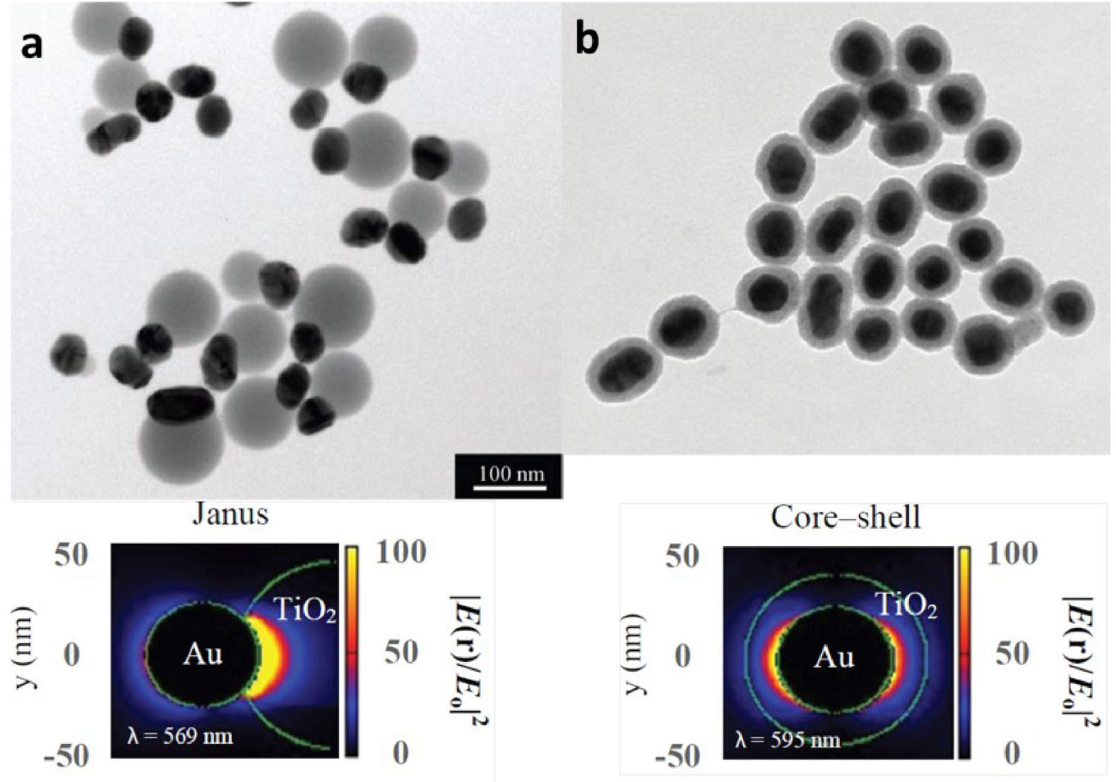
She et al. [86] studied the Au/TiO2 heterostructure with Janus and core–shell nanoparticles. They established that the light absorption was amplified by 1.7 times with Janus nanoparticles compared to core–shell ones.
The improvement of metal-oxide photocatalytic activity in the visible range can also be performed by doping the last with other elements, but the plasmonic strategy is easier to control and leads to equal or improved results. However, a major drawback of having metallic nanoparticles decorating the photocatalysts must be mentioned. It concerns the loss of photocatalyst’s specific surface area exposed to the external medium. The surface coverage of nanoparticles must be tightly controlled in order to avoid an undesired passivation of the photocatalyst. It has been shown that a surface coverage of more than 15% of metallic particles impairs the final photocatalytic properties [94, 102, 103].
5. Light management approaches
The light management approaches attract considerable attention in photovoltaics. This strategy mainly targets two goals: anti-reflection (AR) and absorption enhancement. Given that, the increase of light absorption would be also relevant for the photocatalysis.
Fundamental studies on the anti-reflection principles were already well investigated on bulk materials. The maximum of achievable absorption on solar cells was determined to be 4n2, known as Yablonovitch or Lambertian limit (where n is the refractive index of the semiconductor material). This limit was determined by Yablonovitch and Cody based on Lambertian scatter [104, 105]. Various studies intend to reach this limit and photonic structures have been considered to go beyond this theoretical limit. It was shown that the use of periodic structures could increase the density of optical modes [106, 107, 108, 109, 110]. Therefore, the key parameters determining the interaction light/material are spacing, spatial arrangement, and optical properties of materials [110]. Some publications even underlined the importance of geometry that may predominate intrinsic material properties [111]. This phenomenon is based on the light scattering and reflection on periodic nanostructures which increases the optical path. Therefore, the commonly used light management approaches are mainly based on patterned micro- and nanostructures arrays, their shape, size, and spatial arrangement. For instance, concave nanonets and nanobowl arrays significantly improve light scattering, while vertical nanostructures such as nanocones enhances the anti-reflection properties (Figure 18) [112].
Schematic representation of main light management strategies based on patterned micro- and nanostructure arrays [112].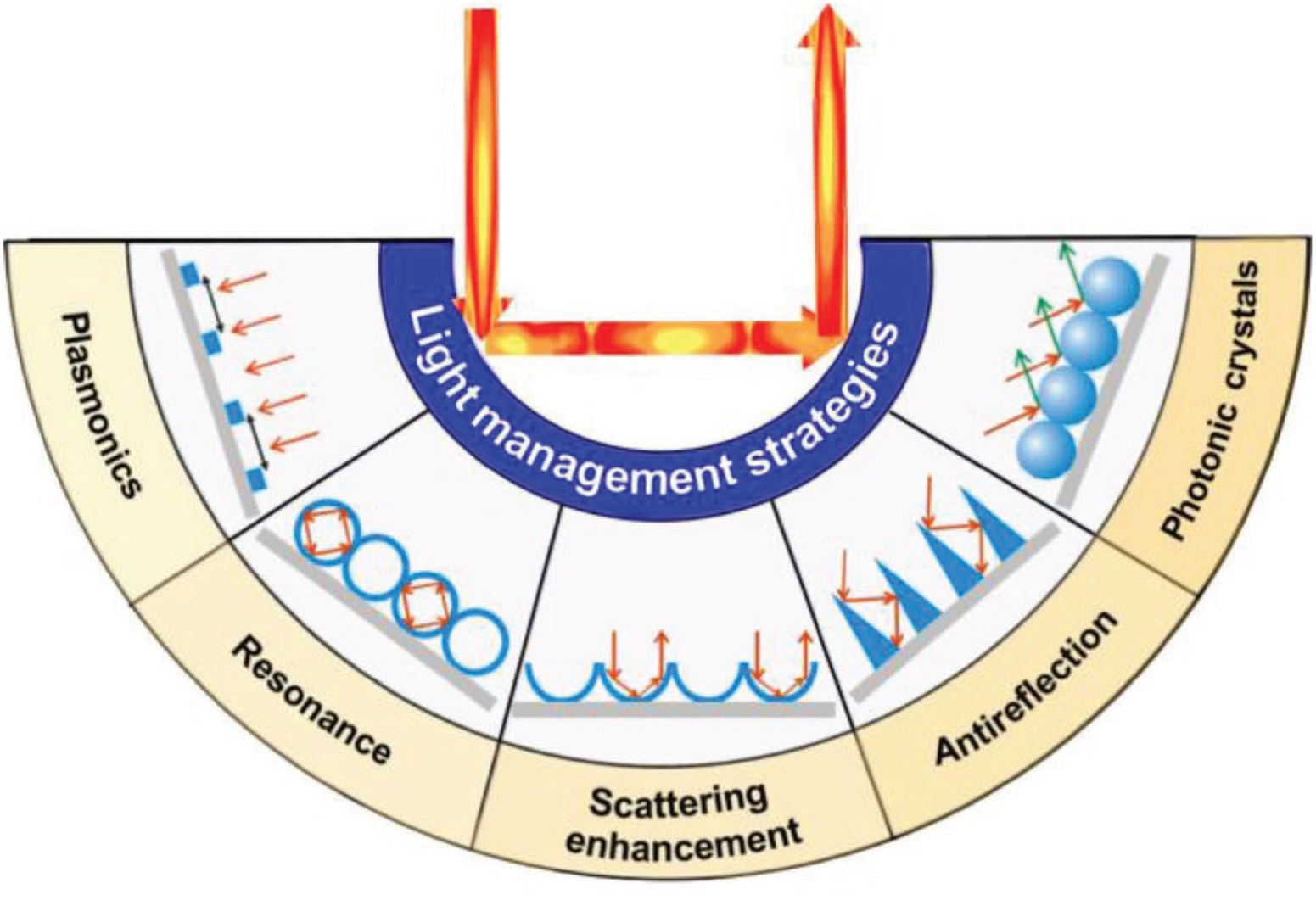
Illustration of light scattering textures: shallow structures (a); structures with higher aspect ratios (b); nanowire designs (c) [113].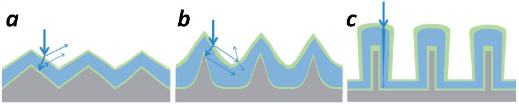
The light scattering enhancement on patterned arrays is related to the increase of the light path due to multiple reflections and refractions. The importance of the aspect ratio of textured surfaces could be evidenced by using the example of Haug et al. [113]. The patterned structures with higher aspect ratio reduce the reflection losses (Figure 19b) compared to shallow structures (Figure 19a). The vertical nanowire designs show up the interest as the potential design for axial absorption paths which is much longer than the film thickness (Figure 19c).
Besides the light scattering strategies, the anti-reflection approaches play an important role to improve the performance of photocatalysis, photovoltaics, optoelectronic, and optical devices. The sharp nanostructures such as nanocones, nanoneedles with dimensions below the light wavelength act as an anti-reflective coating (ARC) [110, 111], whereas the nanostructures with uniform diameters such as nanowires show fundamental photonic resonant modes and could lead to the efficient light confinement and absorption [111].
Typically, in the vertical patterned array the light is trapped by the gap between the vertical structures and if the size of individual structures (the pitch and the depth) are in the same range as the wavelength it leads to the significant decrease of the reflectance in the visible range. In the case if the size of vertical structures is significantly lower than the wavelength range, the incident light is insensitive to these structures that allows to adapt gradually the refractive index independently on the angle of incidence [112, 114].
(a) Moth-eyes photograph; (b) SEM image of the details of ommatidia. The inset figure is a magnified SEM image to show the subwavelength structure array in one ommatidium (the scale bar inset is 1 μm). (c) Measured angle-dependent reflectance on fabricated nanostructures at different incidence angles. (Curves a–e represent incidence angles of 0°, 30°, 50°, 60°, and 75°.) [115].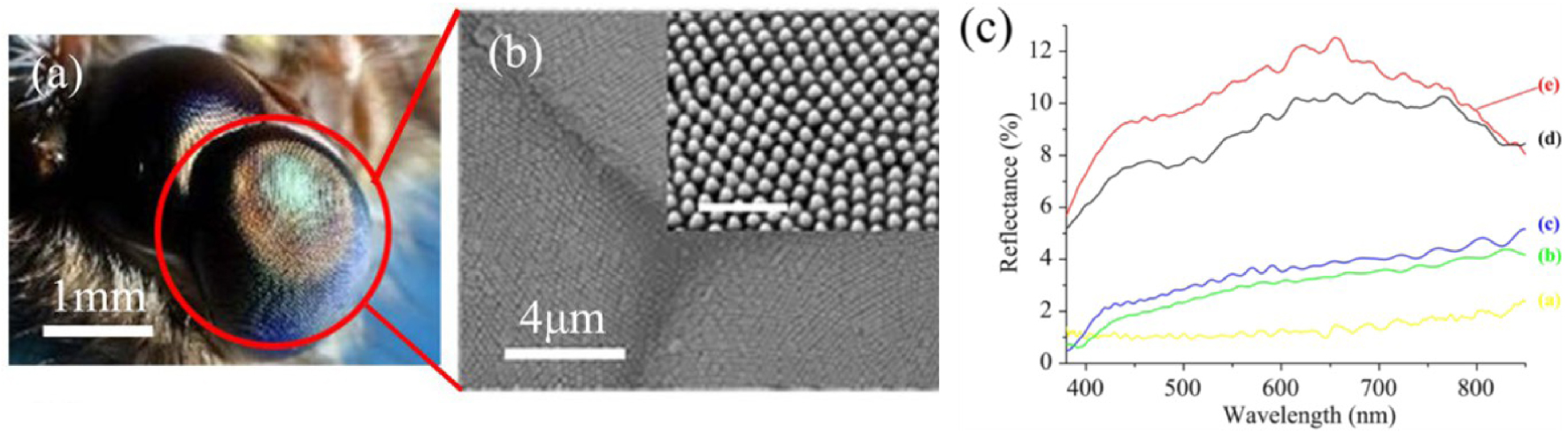
Recently, the nature inspired approach of the Moth-eye gains significant attention due to a relatively simple fabrication approache and high AR efficiency [115, 116]. This biomimetic approach tends to reproduce the surface of the moth eye which present the array of 200 to 300 nm sized pillars (Figure 20). Such surface texturation allows to reduce the reflection of light and enhance night vision capability [115]. Through the fabrication of polymeric pillars on polycarbonate substrates, Sun et al. [115] achieved an average reflection of 1.21% in the visible light range from 380 to 760 nm, at normal incidence and below 4% at 50° of incidence angle (Figure 20c). A similar approach has been reported by Yoo et al. [116] based on patterned SiO2 nanopillar arrays coated with 100 nm of low-reflective index material MgF2 (n = 1.38). Associated with a perovskite solar cell (PSC), SiO2∕MgF2 patterned surface demonstrate increase of the power conversion efficiency (PCE) by 12.50% [116].
The biomimetic approaches based on photonic structures attract particular attention for development of sustainable technologies; they often offer simple and efficient solutions. Low et al. [117] demonstrates the application of the bio-inspired photonic crystals for a photocatalytic CO2 reduction system. Authors inspired by the Papilio nireus wing photonic structures, performed a multilayer porous TiO2 anodized membrane, produced under alternately changing anodization conditions. Such a multilayer photonic structure represents the periodic variation of pore diameters from 80 nm and 100 nm with layer thickness of 200 and 250 nm, respectively (Figure 21). The investigated TiO2 photonic crystals (PCs) demonstrate a significant increase of the CO2 reduction rate (almost 5 times) compared to simple TiO2 nanotube arrays (NTAs) without pore diameter variation.
(a) Schematic illustration of the enhancement mechanism for the photocatalytic CO2 reduction on the TiO2 PCs; (b) gas chromatogram for the product of photocatalytic CO2 reduction test using TiO2 PCs; (c) comparison of the photocatalytic CH4-production activity of P25, TiO2 NTAs, and TiO2 PCs [117].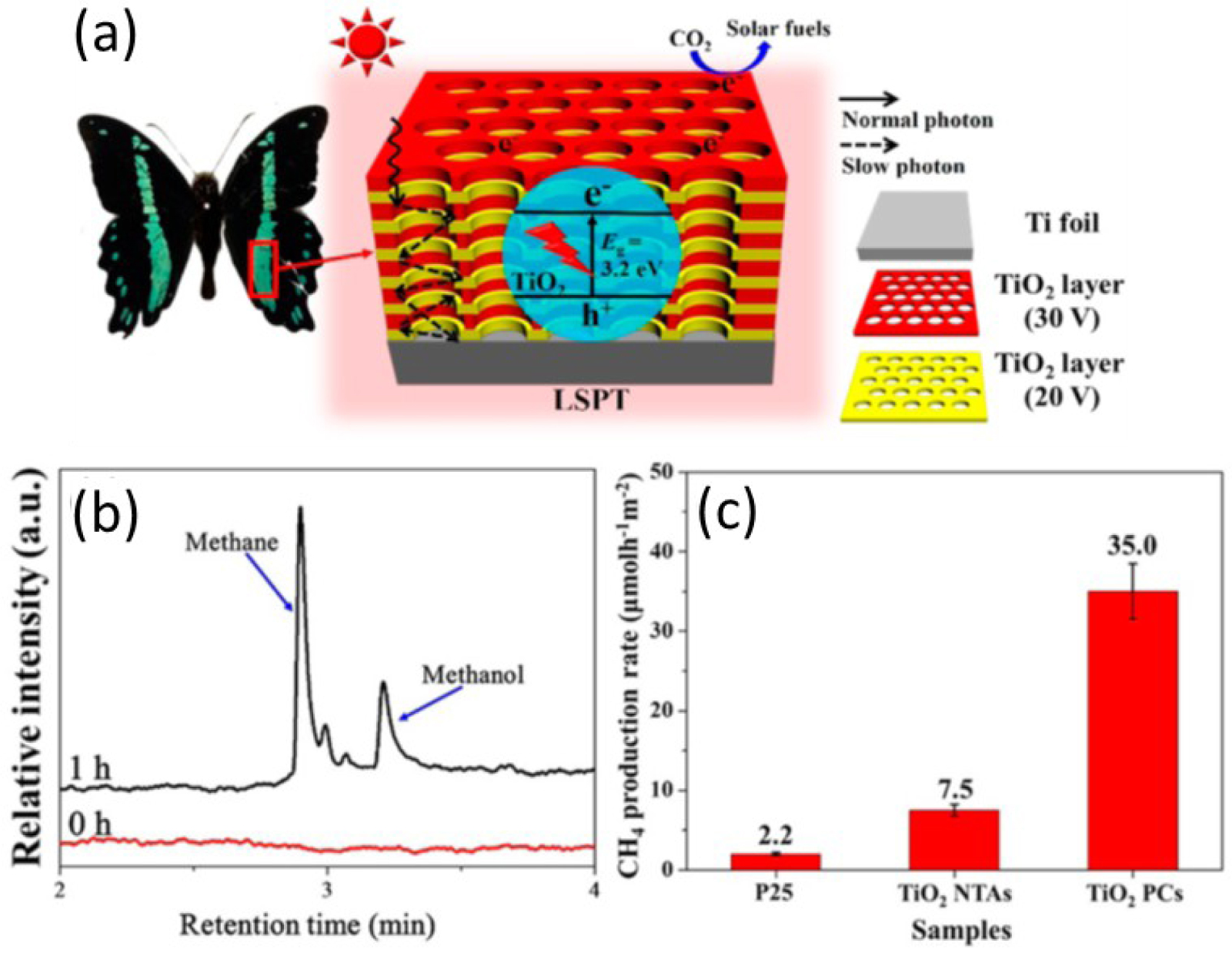
Light management strategies demonstrate a remarkable improvement of the light–matter interactions for all light-related applications. The appropriate design of the array’s geometry, shape, size, spatial arrangement, and the material properties will allow an increase in the efficiency of the light path through scattering, reflection management, light confinement, or waveguiding.
6. Conclusions on photocatalysis enhancement approaches
The overview of the current state of photocatalytic materials and devices summarizes possible paths to enhance the degradation efficiency of photocatalysts. In addition to the photogeneration and transport of carriers, photocatalysis is a surface-dependent approach. Therefore, it is also obvious that the increase of specific surface area would increase the photocatalytic activity. Thus, two kinds of nanoscale photocatalysts can be distinguished: suspensions of nanostructures in solutions or nanomaterials supported on appropriated templates. The main advantages of dispersed nanostructures are the simplicity of use and their low cost. Nevertheless, nanomaterials dispersed in solution tend to agglomerate, lowering their exposed specific surface area. Moreover, due to the toxicity of the nano-objects, they have to be removed after the pollutant’s degradation cycle; thus an additional filtration step is needed. For this reason, there is a growing interest in supported nanomaterials. To increase the exposed specific surface area of nanotextured photocatalysts, their synthesis at the surface of porous supports like membranes has been envisioned for water treatment [118, 119] or water splitting [120]. The conventional photocatalytic approach, which uses basic metal oxides such as TiO2, ZnO, SnO2, is far from reaching the required efficiency. Light absorption limited to the UV range and fast recombination of photogenerated carriers are the main bottlenecks.
Various solutions were proposed to overcome these limitations. Among these solutions, the most commonly used have been previously discussed. The direct band gap engineering via doping intends to lower the band gap energy by the creation of additional energy levels. It will extend the light absorption in the visible range. The assembly of metal oxides with plasmonic nanoparticles also allows the activation of conventional photocatalysts in the visible range. Moreover, this approach improves the photocatalytic activity in the UV range by electron trapping. The semiconductor/semiconductor heterostructure approach acts on the carrier separation. The light management approach is already applied in the field of photovoltaics; it would be also interesting for the photocatalytic applications as a way of light absorption improvement. The periodic organization of metal-oxide nanostructures with a high refractive index offers myriad possibilities of light manipulation. Nevertheless, the methods allowing the metal-oxide structuration in the periodic arrays at deep subwavelength scale are expensive, especially for TiO2 and SnO2. Therefore, it is an open challenge to develop large-scale and low-cost methods of periodic doped metal-oxides nanostructures over highly reflective substrates and to combine them with well- and periodically organized plasmonic nanoparticles.