

1 Introduction
While the development of sol–gel-type chemical solution deposition (CSD) processes for optical coatings of glass by SiO2 and TiO2 dates from the mid-20th century [1,2], the first chemical solution deposited electronic oxide thin films were prepared only as recently as the 1980s. Publications by Fukushima and co-workers [3] on metallo-organic decomposition (MOD), and Budd et al. [4,5] on the sol–gel processing of thin films of lead zirconate titanate (PZT) were among the first that demonstrated the formation of perovskite-type oxides as thin films that possessed the desirable properties of the corresponding bulk materials. The early work by these investigators, and others, led to a rapid expansion of research in this area [6,7]. Since these initial studies, a wide variety of perovskite-related compounds have been synthesized as thin films by CSD techniques. The electronic oxides that have been prepared to date include ferroelectrics and dielectrics based on simple perovskites, such as PbTiO3 (PT), BaTiO3 (BT), and SrTiO3 (ST), as well as solid solutions and complex perovskites, such as (Ba,Sr)TiO3 (BST), Pb(Zr,Ti)O3 (PZT), Sr(Zr,Ti)O3 (SZT), Ba(Zr,Ti)O3 (BZT), Pb(Sc,Ta)O3 (PST), and Pb(Mg1/3Nb2/3)O3 (PMN). Layered perovskites, such as SrBi2Ta2O9 (SBT), SrBi2Nb2O9 (SBN), and (Bi1–xLax)4Ti3O12 (BLT), have also been prepared, as have electronically conducting materials, (La,Sr)CoO3 (LSCO) and (La,Sr)MnO3 (LSMO), as well as high temperature superconducting (HTS) compounds, namely, YBa2Cu3O7–δ (YBCO). In addition thin film proton conducting materials, such as Y doped BaZrO3 (e.g. BaZrxY1–xO3) have been fabricated. Among these compounds, BT, BST, PZT, and SBT are the most relevant for the scope of this review and will therefore be considered in more detail.
Fig. 1 illustrates the typical CSD process together with a number of variations that are frequently employed. The process starts with the preparation of suitable precursors that are often salts, typically, carboxylates, or other metallo-organic compounds, usually, alkoxides (Section 2). The precursors are dissolved in appropriate solvents and mixed in a stoichiometric ratio that yields the desired composition of the final film. Compositional corrections with respect to the exact perovskite stoichiometry are required if: (1) losses occur due to the volatility of a component (e.g., PbO); (2) losses due to component diffusion into the substrate (e.g., Bi loss from SBT) take place; or (3) deliberate off-stoichiometry is desired for the generation of secondary phases or native point defects. In some cases, additives such as chemical stabilizers are included during solution synthesis and additional processing steps, such as refluxing, are employed to adjust the properties of the coating solution (Section 3). The next processing step is deposition of the coating solution on the substrate by spin coating using a rotating substrate, spray coating the misted solution, or dip coating in a solution bath (Section 4). Subsequently, the (wet) as-deposited film is dried (Section 5), pyrolyzed (Section 6), crystallized, and (optionally) post-annealed for further densification or microstructure manipulation (Section 7). The term ‘pyrolysis’ is normally defined as the conversion of solid organic materials, into gases and liquids by indirect heat under exclusion of air, or oxygen, respectively. The material within the reaction chamber is heated to temperatures between 400–800 °C. The pyrolysis process is sometimes referred to as thermolysis. This is merely a preference in the choice of terminology. Although the process reaction volatizes and decomposes solid organic materials by “heat”, the Greek translation of ‘pyro’ is ‘fire’, whereas ‘thermo’ is more correctly, ‘heat’. Thus, thermolysis. Hence in case of the CSD technology, the term pyrolysis is predominantly used to describe the decomposition of the organic matrix in air or oxygen. Often, individual processing steps such as gel formation and organic removal cannot be separated, as implied in Fig. 1. The conversion of the wet, as-deposited film into the desired crystalline film is induced through controlled thermal processes, which typically employ either a hot plate and conventional furnace, or a rapid thermal annealing (RTA) oven. Depending on the specific CSD route and film deposition method, numerous variations in thermal processing conditions are utilized. For example, if the desired film thickness is not obtained in the first coating cycle, the deposition and thermal process sequence are repeated to prepare thicker films. When the desired film thickness is obtained, a final thermal treatment at a still higher temperature may be employed to initiate crystallization, to improve microstructure, or to increase film density.
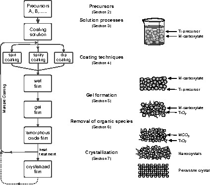
Flow chart of a typical chemical solution deposition (CSD) process. The bars describe the status during the CSD procedure, while the arrows indicate the treatment and the internal processes. On the right-hand side the structural status of the molecules and the ions, respectively, for the evolution of a metal titanate perovskite is schematically depicted.
A range of requirements must be fulfilled by the solution chemistry, substrates, and processing conditions for successful implementation of the CSD technique. These include:
- • sufficient solubility of the precursors in the solvent to form a stable coating solution;
- • synthesis of precursors that decompose or may be pyrolyzed without undesirable residues during thermal processing; i.e., all of the elements except the cations (and oxygen ions) must be released into the gas phase during thermal treatment for perovskite formation;
- • no macroscopic phase separation of precursor components during drying or pyrolysis; i.e., crystallization of the individual components upon solvent evaporation should be avoided and homogeneity at an ‘atomic’ level should be retained;
- • acceptable wetting of the substrate;
- • solution rheology adjusted to the deposition approach and the deposition parameters employed to avoid thickness variations (striations);
- • no crack formation or compositional non-uniformities during pyrolysis or crystallization;
- • minimal interdiffusion of film and substrate constituents; minimal degradation of substrate properties during film processing;
- • sufficient long-term stability of the solution to avoid non-reproducible film properties that are dependent on solution aging.
If these requirements are fulfilled and if processing conditions are optimized, the CSD technique represents a rapid and cost-effective method for synthesizing high-quality electronic oxide thin films. In this article, the CSD processing of a number of materials mentioned above will be reviewed, with an emphasis on understanding the underlying chemical and physical aspects of the solution preparation, film deposition, and crystallization aspects of the process.
2 Precursors
The general principle involved in the solution deposition of perovskite films is to prepare a ‘homogeneous’ solution of the necessary cation species that may later be applied to a substrate according to the requirements listed above. The requirements of appropriate solubility combined with pyrolysis that leaves solely the cations (and oxygen) as a residue, represent an especially significant limitation regarding the choice of precursors. Usually, metallo-organic compounds are suitable, due to the fact that their solubility in polar or non-polar solvents can be tuned by modifying the organic part of the molecule, and because the organic moiety pyrolyzes in oxidizing ambient atmosphere without residue. Before describing the various solution deposition routes and characteristics, the most commonly used classes of precursor compounds will be outlined briefly. For a basic understanding of the background chemistry, the reader is referred to standard introductory texts [8]. Details on precursor chemistry are also found in [9–12].
2.1 Carboxylates
Metal carboxylates are salts of carboxylic acids, R–COOH, where R represents an alkyl group such as methyl, CH3 (acetic acid; salt: acetate), ethyl, C2H5 (propionic acid; salt: propionate), etc. The polar nature of the salt is indicated by the charges shown in the illustration for Ba acetate, as an example (Scheme 1):

Carboxylates can normally be dissolved in their own (parent) carboxylic acids, and for short alkyl chain salts, some solubility of the carboxylate (i.e., acetate, R = CH3) in water and other highly polar solvents is typically observed due to the polar nature of the salt. Regarding the water stability of short chain carboxylates, it should be noted, that solubility typically implies that these materials are not stable in water. However in case of CSD processing stability against water means that it does not lead to a gel formation upon addition of water in contrast to the metal alkoxides. Long, non-polar alkyl chains lead to carboxylates (e.g., 2-ethylhexanoates, R = C7H15) that are soluble in non-polar solvents, such as xylene. Chemically, carboxylates are stable against water [12] and oxygen, and in the processing of ferroelectric thin films, they are often employed as precursors for lower-valent, ionic cations such as Pb2+, Sr2+, and Ba2+.
2.2 Alkoxides
Alcohols (R–OH) can be regarded as very weak acids, and the metal salts of alcohols are called alkoxides, M(OR)x, where M is a metal. Due to their polar M–O bond, non-stabilized alkoxides are very sensitive toward hydrolysis, leading to the formation of metal hydroxides (M–OH) with the concurrent release of an alcohol molecule:
If hydrolysis is extensive, precipitation of hydroxide or oxide/hydroxide species may occur. However, the goal in the use of these precursors for film formation is to control the hydrolysis and subsequent condensation reaction (shown below). If properly manipulated, these reactions lead to the formation of short chain polymeric species referred to as oligomers.
Alkoxides can be stabilized toward hydrolysis if their organic part R contains further polar groups such as ether linkages, R–O–R′ (e.g., 2-methoxyethanol), amine groups, –NH2, keto groups >C=O, or further alcohol groups, >C–OH (e.g., 1,3-propanediol); see Scheme 2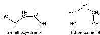
2.3 β-diketonates
Organic molecules with two keto groups separated by one methylene group (–CH2) are called β-diketones. These molecules undergo an internal hydrogen exchange reaction (keto-enol tautomerism), which converts one of the keto groups into an alcohol group according to (Scheme 3
Via the alcohol group, metal alkoxides may be formed which are strongly stabilized by the additional keto group due to the chelate effect, and even more, due to the delocalization of the electrons in the 6-membered ring (see Scheme 4
2.4 Mixed ligand precursors
Mixed-ligand precursors are also frequently employed in CSD processing. For example, titanium tetraisopropoxide, Ti(OiPr)4 (iPr = i-propyl, –C3H7), which is too reactive to be directly employed in most CSD routes, may be converted into a more suitable precursor by a reaction with either two equivalents of acetic acid or acetylacetone (Hacac). Such reactions are critical in dictating precursor characteristics and have been studied extensively. Others have precipitated crystalline compounds from these reactions for subsequent use as precursors for solution preparation [13]. Mixed ligand molecules (carboxylate-alkoxide [14] and diketonate-alkoxide [11], respectively) represent complexes that are not easily hydrolyzed by water.
2.5 Mixed metal precursors
To control the extent of intermixing and stoichiometry of the precursor species, there have been a number of investigations to synthesize stoichiometric, mixed metal precursors with structures similar to the perovskite crystal structure. The motivation behind these efforts is that stoichiometric precursors with structures similar to the desired crystalline phase should undergo crystallization at lower heat treatment temperatures, thereby reducing problems with substrate/film interactions and substrate degradation. However, most attempts in this area have resulted in mixed metal species with a cation stoichiometry different than that of the perovskite material. Examples in the synthesis of PbZrO3 and PbTiO3 include [PbZr2(μ4-O)2(OOCCH3)4(OCH2CH3)6]2 and [PbTi2(μ4-O)(OOCCH3)(OCH2CH3)7]2 [15,16]. The formation of these compounds indicates the importance that thermodynamic sinks can play in the synthesis of mixed metal compounds [17–19]. However, the fact that the cation stoichiometry of the precursor species is not identical to the crystalline perovskite phase (and in fact, likely varies from one precursor molecule to another) has not prevented the production of high quality thin films by CSD, as is discussed in greater detail below. In addition, it is worth noting that it has not been demonstrated conclusively that the perovskite formation temperature of films prepared from stoichiometric precursors is significantly lower than those prepared from single-cation precursors. This may be due to the fact that, during processing, the precursor molecule is destroyed prior to the formation of the perovskite phase. Thus, the formation temperature may depend more critically on the stability and reaction pathways of the intermediate phases rather than the structure of the original precursor molecule.
3 Solution processes and chemical routes
The coating solution is prepared by mixing, and possibly reacting (heating or refluxing), the individual precursors or precursor solutions. The chemical interactions that occur between the starting reagents during solution synthesis will depend on the reactivity of the compounds and the solution preparation conditions, such as reflux temperature. In classical sol–gel processing routes (see below), the reactivity of the reagents is high, and if alcohol exchange occurs, or if modifying ligands are used, the structure of the species in solution can bear little resemblance to the starting compounds [20]. In this case, the species that are generated are frequently oligomeric in nature and can contain more than one type of cation [15,16,21,22]. In contrast, for long-chain carboxylate compounds, such as zirconium 2-ethylhexanoate, which have been historically used in MOD routes [23], reactivity is low and the chemical interactions between the different precursor compounds is minimal. In addition to manipulation of reaction conditions to control precursor species characteristics, the viscosity, solute concentrations, and solvent system must also be adjusted at this stage for the coating technique that will be employed and the type of substrate.
Depending on the procedures utilized during coating solution preparation, the gelation behavior of the deposited film, and the reactions that take place during thermal annealing, the various chemical routes utilized for electronic oxide film fabrication can be grouped into three principal categories:
- • classical sol–gel processes that use alkoxide precursors that undergo primarily hydrolysis and polycondensation;
- • metal organic decomposition (MOD) routes that utilize carboxylate precursors that do not undergo significant condensation reactions during either solution preparation or film deposition;
- • hybrid routes that exhibit condensation reactions at several process stages; frequently, this route is used when multicomponent oxide films, e.g., perovskite materials, are prepared from multiple precursor types or when chelating ligands are added to solutions with multiple precursor types.
Certainly, these categories are too imprecise to classify all conceivable CSD routes exactly, and in many cases, the route under study comprises aspects of more than one of these categories. However, to understand the underlying chemistry of a particular CSD route, it is beneficial to discuss the various approaches that have been utilized from this standpoint.
3.1 Sol–gel processes
In the sol–gel processing of silica, the alkoxide TEOS (tetraethylorthosilicate) and the solvent ethanol are utilized most frequently. For perovskite films, however, the solvent, 2-methoxyethanol (CH3OCH2CH2OH), has been used most extensively. Deposition routes based on 2-methoxyethanol [4,5] are most appropriately considered as sol–gel processes because the key reactions leading to the formation of the precursor species are hydrolysis and condensation, in which metal–oxygen–metal (M–O–M) bonds are formed:
- • hydrolysis
- • condensation (alcohol elimination)
- • condensation (water elimination)
In processes in which multiple alkoxide compounds are used, pre-hydrolysis of the less reactive alkoxide may be employed to improve solution compositional uniformity.
Another key reaction in the use of this solvent is the alcohol exchange reaction that occurs, resulting in a decrease in the hydrolysis sensitivity of starting reagents such as zirconium tetra n-propoxide and titanium tetra i-propoxide used in the production of PZT films:
Alcohol exchange
It has also been demonstrated that through manipulation of the above reactions, i.e., by controlling the reflux, catalysis, and hydrolysis conditions, the nature of the resulting solution precursors and gels may be controlled, allowing for control of material properties. Many of the catalyst (acid or base) and hydrolysis effects in perovskite materials parallel those for silica sol–gel processing using TEOS [24]. For example, in the production of lead titanate gels, acidic catalysis conditions resulted in gels that seemed more capable of polymeric rearrangement, while gels prepared under basic catalysis conditions exhibited more phase separation and were more highly textured [25]. Other physical properties, namely, surface area and pore characteristics, of gel-derived lead titanate powders also indicate a strong similarity to silica [26]. Solutions prepared with higher levels of hydrolysis resulted in powders with greater surface areas and pore volumes.
Solution processes based on the use of methoxyethanol are widely used, due to the ability of this solvent to solubilize a variety of different precursors. When properly carried out, the process offers excellent control and reproducibility of process chemistry, and non-hydrolyzed solutions exhibit minimal aging effects. Thin films with excellent properties have been prepared for a number of materials including PZT [5], LiNbO3 [27], BaTiO3 [28,29], and YBCO [30]. However, for the non-chemist, the procedures involved can be rather complex. Further, 2-methoxyethanol is a known teratogen, which presents a significant safety concern and inhibits its use in most manufacturing facilities. Hence 2-butoxyethanol, which is less toxic, has been introduced into the CSD processing of PZT thin films [31].
3.2 MOD solution synthesis
The second solution-synthesis approach that is widely employed for perovskite film formation, metallo-organic decomposition (MOD), has historically used large carboxylate or β-diketonate (acac-type) compounds, such as lead 2-ethylhexanoate, zirconium neodecanoate, and titanium di-methoxy di-neodecanoate [23]. The basic approach consists of simply dissolving the metallo-organic compounds in a common solvent, usually xylene, and combining the solutions to yield the desired stoichiometry. For solution preparation, investigators have used commercially available as well as in-house synthesized precursors [32]. Since the starting compounds are water-insensitive, they do not display the oligomerization behavior discussed above, and the precursor species that exist in solution retain a strong resemblance to the starting molecules. This aspect of the process, together with the use of non-interacting solvents, allow for the characterization of the solution as a simple mixture of the starting compounds. Solution synthesis is straightforward, and the approach allows for rapid compositional mapping of material systems. It has been used for a number of ferroelectric materials [33–35], as well as for high temperature superconductors [36] and colossal magnetoresistive (CMR) films [37]. The MOD route has also received additional attention in the preparation of Aurivillius phase SrBi2Ta2O9 and related materials, which are potentially alternative candidates to Pb(Zr,Ti)O3 for ferroelectric non-volatile RAM devices. The 2-ethylhexanoates of Sr, Bi, and Ta are dissolved in an excess of 2-ethylhexanoic acid and xylene, which is used to adjust the solution viscosity [38].
While the MOD process is straightforward, it possesses a number of limitations. First, the large organic ligands may cause cracking during thin film processing due to the excessive weight loss and shrinkage that can occur. To circumvent this, control of solution concentration and thermal processing is required. Second, the minimal reactivity of the starting reagents may present a further limitation. Because precursor characteristics can exhibit dramatic effects on thin film properties, the inability to ‘tailor’ the properties of the low-reactivity starting compounds restricts process flexibility. Hence, control of structural evolution and film microstructure becomes limited to variations in solvent, solution concentration, and film deposition and heat treatment conditions.
The standard MOD process using large carboxylate compounds is still widely employed, but Haertling has developed an alternative MOD strategy that minimizes the first problem discussed above [39]. In this process, low reactivity starting reagents are again employed, but in this case, short chain carboxylate (e.g., acetate) and strongly chelating β-diketonate (e.g., acac) compounds are used, rather than the more commonly employed 2-ethylhexanoate and di-neodecanoate precursors. The use of chelating ligands such as acac can lead to the formation of monomeric compounds and the lower organic content of the precursors reduces film shrinkage after deposition, decreasing problems with film cracking. Films with properties comparable to those prepared by sol–gel and hybrid processes are obtained. The compounds used are both water-insensitive and commercially available and solution synthesis is straightforward for the non-chemist. Although the solutions are water-insensitive, the presence of acetate ligands in an alcoholic-based solution still results in esterification. Solutions, therefore, still exhibit aging and display changes in film properties as a function of time. However, the aging rates are slower than those determined for hybrid processes [40].
A further example of using short chain carboxylate precursors in MOD processing for the deposition of collosal magnetoresistive (CMR) compounds such as La1–x(Ca,Sr)xMnO3 has been developed by Hasenkox et al. [41]. In the so-called APP-route, the propionates of all compounds are dissolved in propionic acid. This type of solutions can be easily prepared, have very good long-term stability, and yield excellent films. Even epitaxial films (see section 8) can be prepared by this route. Materials such as LaNiO3 and La1–x,SrxCoO3 have also been successfully prepared using this route [42,43].
3.3 Hybrid processes
Many synthesis approaches start from short-chain carboxylate A-site precursors dissolved in an excess of carboxylic acid (e.g., acetic acid) and B-site alkoxide compounds. These processes are referred to as ‘hybrid’ because they utilize both carboxylate and alkoxide precursors, and the B-site alkoxides react with the carboxylic acid to form oligomers or small polymers according to (for example, Scheme 5
Hybrid routes also include “chelate” processes because the chelation reaction shown above is key in defining the properties of the resulting precursor solution. The carboxylic acid also serves as a solvent to dissolve the A-site carboxylate, which is typically only slightly soluble in alcohols such as methanol, ethanol, or propanol. In the development of these processing routes, a variety of carboxylic acids, including acetic acid and propionic acid have been evaluated [44,45], and PZT, BT, ST, and other materials have been prepared.
Typically, the acetate, or in general, the carboxylic acid groups, coordinate the B-site metal species in a bidentate fashion, and frequently act as bridging ligands, linking metal centers together to form oligomers. Chelation of the B-site alkoxides by these carboxylate groups result in the formation of precursors that possess reduced sensitivity toward hydrolysis. Other additives, such as acetylacetone (Hacac, 2,4-pentanedione), have also been employed. Again, these additives serve to reduce the sensitivity of the alkoxide compounds to hydrolysis. A review of the use of carboxylic acids in the preparation of ceramic powders is given by Lessing [46] and the modification of metal alkoxides with β–diketonate compounds has been discussed by Hubert-Pfalzgraf [21,47].
The reactions that occur during BT and PZT solution preparation in hybrid processing have been extensively studied using spectroscopic techniques [48–50]. Similar reactions to those that occur in sol–gel processing apparently take place. As discussed by Hennings for the hybrid processing of BaTiO3 [48], the precursors formed for lead zirconate titanate and lead titanate are small oligomers [20,51] and as for sol–gel processes utilizing 2-methoxyethanol, the reaction pathways associated with chelation and other reactions in hybrid solution synthesis apparently do not result in the incorporation of the A-site precursors into the oligomeric structure. Instead, the A-site species may be adsorbed or occluded on the surface of the B-site oligomers [48]. This result has also been confirmed in sol–gel processing of PZT gels by EXAFS studies, which have indicated that the A-site precursor is probably not intimately involved in the formation of the gel network [52]. For both processing routes, it therefore appears that the precursors are chemically heterogeneous on an atomic scale. Arčon et al. [53] extended the EXAFS technique to the quantitative analysis of PZT precursor solutions. They found that the nearest neighborhood is the same in all cases and constitutes two oxygen atoms for lead and six for zirconium. Significant differences introduced by the choice of the lead source and by drying are found in the metal-metal correlation in the second shell. In contrast to Sengupta et al. [52], Pb–O–Ti and Pb–O–Zr linkages, at least in the precursor solutions, have been definitely established. Hence, EXAFS offers the possibility to obtain detailed insight into the processes occurring on the pathway from the early liquid phase to the final crystalline film.
Compared to the typical 2-methoxyethanol process, hybrid processes offer the advantages of relatively simple solution synthesis; involved distillation and refluxing strategies are normally not required. Representative chelate processes are described by Hoffmann and Waser [45], Yi and coworkers [54], and Schwartz et al. [55]. In the production of BT films, barium acetate or propionate is typically dissolved in the parent carboxylic acid, and the B-site alkoxide is then added [44,48,56]. Alcohol and water may then be added for control of solution viscosity and stability, though additional reactions likely occur upon the addition of these reagents. While chelate processes are simple and rapid, the chemistry involved in solution preparation is quite complex, due to the number of reactions (chelation, esterification, hydrolysis, and polymerization) that occur. These have been studied in detail for PZT processing by Nuclear Magnetic Resonance (NMR) and Fourier Transform Infrared (FTIR) spectroscopy [49]. The complexity of the reactions results in a diminished ability to control precursor structure compared to true sol–gel approaches, and thus, the gain in process simplicity comes at a cost.
Another disadvantage of chelate processes is that continued reactivity in the precursor solution following synthesis can result in a change in precursor characteristics over time (weeks to months), and thereby, degrade film properties. This occurs because substituent groups such as acetate, while less susceptible to hydrolysis than alkoxy groups, may still be attacked by water, resulting in a change in molecular structure. This reaction, continued esterification of the solution, and other reactions result in continued oligomerization and realkoxylation of the species, eventually causing precipitation. Using spectroscopic and analytical techniques, Boyle and co-workers have documented the timescale of such processes and their impact on PZT film properties [50].
In spite of these disadvantages, as with sol–gel processes, thin films with excellent electrical and microstructural properties have been prepared by this approach, and a number of research groups routinely use it as their primary method of film fabrication. These results, together with those for 2-methoxyethanol-based processing, would therefore seem to indicate that complete homogeneity/stoichiometry of the individual precursor species is not required for the preparation of high quality materials, provided the interdiffusional distances are sufficiently short [52].
3.4 Diol and suspension processes
While the hybrid methods described above have been employed successfully for numerous uses, other applications dictate that thicker coatings (1–10 μm) be deposited in fewer deposition steps (1–2 steps per μm). Two general strategies have been developed to attain these thicker coatings. The first approach is based on the solvent/reactant 1,3-propanediol, which is believed to act as a crosslinking agent in this process, resulting in large oligomeric species [57–60]. These large oligomeric species, together with the non-gelling nature of the films allow for an increase in the deposit thickness compared to standard hybrid, MOD, and sol–gel processes. In the fabrication of decoupling capacitors, perovskite layers that are often ~ 0.8-1.0 μm in thickness are desired depending on the operating voltage, required reliability, and electrical breakdown characteristics. By using approaches based on 1,3-propanediol, such films can be prepared in one or two deposition and heat treatment cycles, reducing manufacturing costs [61]. Still thicker coatings have been prepared by using approaches that incorporate solutions with powder particles [62]. This latter method has been used for PZT materials to prepare coatings with thicknesses as high as 30 μm.
3.5 Nitrate, citrate and Pechini routes
While sol–gel, chelate, and MOD processes have been used most extensively for ferroelectric film fabrication, three other processes (Pechini, citrate and nitrate) have also been studied for the deposition of other perovskite thin films. In the Pechini process [63], metal nitrates are first dissolved in water, then citric acid [an α-hydroxycarboxylic acid, HOC(COOH)(CH2COOH)2] is typically added to chelate the metal cations by forming a polybasic acid. When a polyhydroxyalcohol, most often ethylene glycol, HOCH2CH2OH, is then added, the citric acid–metal chelates will react with the ethylene glycol to form organic ester compounds. By controlling the ratio of ethylene glycol to citric acid, it is possible to control the molecular weight of the polymeric species in the precursor solution. Film deposition is carried out using the same procedures as those employed for MOD, sol–gel, and other hybrid processes.
Citrate solution synthesis is similar to the Pechini process, except that ethylene glycol or other polyhydroxy alcohol is not utilized for polymer formation [64]. To produce citrate precursor solutions, stoichiometric amounts of the desired metal nitrates are dissolved in water and citric acid is simply added to form citrate species. Film fabrication is then carried out in the usual fashion. The citrate process results in a solution that has a lower organic content than the Pechini process, and consequently, films that display less weight loss during conversion to the ceramic phase.
Finally, in the nitrate method, the precursor solution is synthesized by simply dissolving the desired nitrates in de-ionized water or alcohol [65]. The method is thus, more straightforward than the Pechini and citrate routes, but two common problems must be avoided: (1) dewetting of the substrate may occur due to the absence of gelation and the extent of hydrogen bonding; and (2) re-crystallization of the starting reagents may take place during film drying. However, the method has been used successfully in the deposition of heteroepitaxial lanthanum aluminate thin films [65].
Recently, a new aqueous solution–gel process for various ferroelectric thin films such as BLT, SBT, SBN, and PZT on platinized silicon substrates has been presented [66,67]. The approach is based on water and chelating carbonic acids like oxalic acid, citric acid and other coordinating ligands, like ethylenediamine. This route has the particular advantage of being inexpensive and the use of organic solvents can be avoided. In addition, the synthetic procedure does not need to be carried out under inert gas atmosphere. However, wetting problems may still occur due to the use of water (poor film-substrate adhesion) as a solvent. Instead of improving surface adhesion by the addition of a surface-wetting reagent, the authors modified the surface characteristics of the platinum film prior to spin coating by either using a dedicated chemical cleaning procedure [66] or a UV/ozone technique [67]. The improved wettability was verified by contact angle measurements.
4 Coating techniques
Once the precursor (coating) solution has been prepared, films are typically formed by spin casting, spraying, or dip coating, as illustrated in Fig. 2. After deposition, the desired ceramic phase is subsequently obtained by heat treatment.
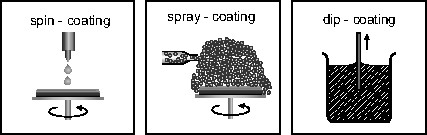
Illustration of the commonly used coating techniques.
At the laboratory scale, spin deposition is usually achieved with a photoresist spinner and the substrate is typically either a planar single crystal oxide, or an electroded Si wafer. The substrate is held in place on the spinner by applying a vacuum to the backside of the wafer through a chuck that is at the end of the spinner motor shaft. The wafer is typically flooded with solution during a ‘static dispense’ using a syringe with a 0.2 μm filter. The wafer is then accelerated rapidly to 1000 to 8000 rpm. The angular velocity and the spinning time, together with the solution viscosity, can be used to control the thickness of the wet film. This characteristic and the solute concentration will, in turn, determine the thickness of the final ceramic film. Birnie has reported solution characteristics and deposition conditions that can result in striation development in the films [68,69].
The spray-coating technique potentially offers the advantage of conformal film deposition on non-planar structures (e.g., steps, stacks or trenches) on semiconductor chips. This technique is based on the transformation of the coating solution into an aerosol by means of an ultrasonic nebulizer or appropriate pressure-driven, nozzle-based atomizer [70,71]. Compared to spin and dip coating, the solution viscosity must be reduced significantly in order to facilitate the nebulizing process and the formation of sufficiently small droplets. The misted solution is transferred into the deposition chamber by a carrier gas where the droplets settle onto the wafer surface by gravitation, or more efficiently, by an electrostatic field. In this later case, the aerosol is electrically charged by a corona discharge before entering the chamber [70,72]. The step coverage and conformal nature of the films deposited on non-planar surfaces by spray-coating has also been studied: for 400-nm steps, films that were ~200 nm thick demonstrated thickness variations of < 20% [70]. The key to improving conformal coverage is reduction of the solution droplet size. By using a Venturi nozzle rather than an ultrasonic nebulizer, it is possible to reduce the droplet size to ~100 nm. However, since the deposition efficiency obtained by gravitation decreases with droplet size, electrostatic enforcement is desirable in this case.
Dip-coating involves the formation of a film through a liquid entrainment process that may be either batch or continuous in nature. Brinker and Scherer present an excellent review of the various factors that govern the dip-coating process [73]. For the batch method [74], the general steps include immersion of the substrate into the dip-coating solution, start-up, where withdrawal of the substrate from the solution begins, film deposition, solvent evaporation, and continued drainage as the substrate is completely removed from the liquid bath [73]. Depending on the rate of substrate withdrawal, solvent volatility and film thickness, the extent of overlap of these different processes can vary dramatically.
The thickness of the film that is formed in dip-coating is governed by factors that include viscous drag, gravitational forces, and the surface tension in the concavely curved meniscus among others [73]. For dip-coating from sol–gel solutions, the characteristics of the precursor (sticking probability), aggregation and gelation behavior also play a key role in defining both the thickness and nature of the film that is formed [73]. To characterize the changes that occur in the nature of the film during the formation process, a variety of probe molecules have been incorporated into the sol [75]. These have allowed for in situ characterization of film/process properties, such as solvent composition in the entrainment and drying line regions, as well as measurements of the drying-induced pressure that is developed [76].
5 Gel formation
Immediately following deposition (either by spin-coating, spraying, or dip-coating) the as-deposited film typically retains a significant organic fraction. Its nature at this stage is highly dependent on the characteristics of the solution precursor species and the solvent. For example, in diol-based processes, the film is wet at this stage of the process, while for more common solvent systems, in addition to the organic moieties associated with the inorganic network, significant amounts of solvent are entrapped. The type of the film that is formed may be described according to the precursor interactions and film gelation behavior that takes place during deposition. The gelled film is, in many ways, similar to the sol, except in chemical gel films (see below), where a more extensive long-range network structure formed. This leads to the gel possessing the properties of a viscoelastic solid; i.e., it is a solid with a low elastic modulus. Gelation of the film typically is driven by solvent evaporation, which forces interactions between the precursor species, and in many instances, chemical cross-linking reactions, depending on the reactivity of the precursor species. For films prepared by spin casting, gelation typically occurs shortly after the spin-off stage of the deposition process [76], and depending on the type of gelation behavior that occurs, three classes of films may be distinguished prior to further thermal treatment.
- • Chemical gel films (also referred to as ‘polymeric’ gels) exhibit polymerization or polycondensation reactions, respectively, during, or immediately after, deposition leading to the formation of chemical bonds between oligomeric species. These films cannot be redissolved in their parent solvents [77]. A proposed gel structure for this class of films is presented in Fig. 3.
- • Physical gel films display gelation through physical aggregation of the oligomers and polymers because of van der Waals forces or steric interactions. It is possible to redissolve these films in their parent solvents [77]. Physical gels often become chemical gels with time, or the application of slightly elevated temperatures, due to condensation reactions.
- • Non-gelling films are characterized mainly by their ‘wet’ appearance after deposition [78]. This behavior is associated with the high boiling and low volatility of the solvent utilized, as well as the low reactivity of the precursor species toward polymerization. Upon heating, solvent evaporation typically occurs at similar temperatures to those where pyrolysis starts.

Ti–O network with adsorbed strontium or barium carboxylate molecules (from [48]).
In addition to influencing film gelation behavior, precursor properties can also significantly impact the densification behavior of the film during later processing stages. A variety of experiments have been carried out to systematically investigate these effects using ‘model’ systems, such as titania and zirconia. These compounds allow for understanding of the processing behavior of perovskite films, such as BT, ST, and PZT, because the behavior of these more complex systems is strongly influenced by the modified B-site precursor species [79]. In general, it was found that lower reactivity precursors, or precursors that demonstrate higher pyrolysis temperatures, generate films with higher densities [77,79]. In hybrid processing, precursor reactivity and pyrolysis temperature may be controlled through the selection of the modifying ligand. Hence, ligand properties, and extent of alkoxide modification, can play a key role in defining film gelation and densification and may be used to manipulate film-processing behavior.
Finally, it should be noted that in addition to precursor properties, solvent choice is also an important consideration for control of film gelation and processing behavior. The solvent that is selected must be suitable, not only for the particular precursor system (dissolution, stability and solution aging behavior), but other solvent characteristics, such as evaporation rate, which can drive gelation, and surface tension characteristics, which can dictate substrate wetting behavior, must also be considered. Therefore, for the design of optimized CSD routes, the selection of the solvent will be dictated by some compromise between these various properties.
As an example, consider the recent work to develop processes that generate thicker coatings that are based on the solvent 1,3-propanediol [57–61,80]. It has been demonstrated that films with thicknesses between 0.5–1.0 μm/deposition can be prepared by this approach, however, the as-deposited films may tend to de-wet the substrate surface, resulting in degradation in film quality [78]. In this instance, the high viscosity of the solvent inhibits both physical and chemical interactions of the precursor molecules, increasing the tendency of the film toward dewetting. However, it is the viscosity of the solvent that makes it possible to obtain the higher film thicknesses. Few other solvents possess the viscosity characteristics needed to generate these thicker coatings and the route has been used effectively for a variety of ferroelectric films [57–61]. ‘Mixed’ solvent systems, such as acetic acid/methanol [55] and propanol/propanediol [80] have also been utilized to obtain the desired balance of properties.
6 Removal of organic species during thermal treatment
To obtain the desired oxide phase, solvent remaining entrapped within the pore structure of the film and the organic moieties associated with the gel network must be removed. Typically, the oxide phase is obtained by heat treatment. Accompanying the conversion into the oxide phase, or perhaps more accurately, at its root, is rearrangement of the gel network through a variety of bond reorganizations and structural relaxation processes that eliminate structural free volume within the film. During this process, M–O-C and M–O-H bonds are broken, and as the associated volatile species are removed, the formation of an M–O-M network occurs. It should be noted that the concept of an amorphous M–O–M network is perhaps somewhat more appropriate for processing of the lead-based materials, where the formation of an amorphous structure may correctly be viewed as a distinct, definitive material state. In the processing of BT, ST, and BST, the formation of relatively refractory carbonate phases complicates this picture; certainly (by definition) these crystalline carbonate compounds form before organic pyrolysis is complete). The general reactions that take place during this transformation include:
- • thermolysis (formation of volatile organic species without oxygen);
- • pyrolysis (formation of volatile organic molecules such as CO, CO2 by combustion);
- • dehydration (or dehydroxylation; elimination of OH groups from the network as H2O);
- • oxidation (formation of M–O–CO2 carbonate species).
Since the carbon and hydrogen contents of the films prior to heat treatment can be in the order of a few weight percent to a few ten weight percent, the changes in the gel network structure that occur at this processing stage can be extensive.
Two approaches are commonly used to complete the transformation of the as-deposited film into the crystalline ceramic: the two-step and the one-step process, which are discussed in greater detail below. Briefly, in the two-step process, the removal of (at least most of the) organic constituents is carried out in a separate processing step (i.e., the first stage of the two step method) at lower temperatures (200–400°C) prior to a high-temperature crystallization step. In the one-step process, organic removal and crystallization are accomplished in the same processing step, which is carried out at temperatures sufficiently high to induce crystallization of the oxide, e.g., the ferroelectric perovskite phase. For both of these processes, to complete the conversion of the as-deposited film into the crystalline ceramic state, complex structural reorganizations that commence with the removal of the organic species are involved. While the specific decomposition pathway will depend on the heating rates and temperatures employed, the type of atomistic rearrangement processes that must occur are illustrated in Fig. 4 for the transformation of a Ti-based oligomeric precursor species [81,14] into rutile. As may be seen in the figure, while the local environment of the titanium species is the same in the oligomer and the crystalline phase, for most of the oxygen species, the coordination environment must change to threefold (O–M3, from either non-bridging (M–O–C) or twofold (M–O–M) [82].

Schematic representation of the transformation of the solution precursor [82] into the desired crystalline phase for TiO2. The open circles represent the oxygen atoms while the titanium atoms are represented by the filled circles (reprinted with permission from [82] copyright 2004 American Chemical Society).
In addition to the rearrangement processes that take place at the atomic level, structural rearrangements at other dimensional scales must also occur, as shown in Fig. 5 for the crystallization of a desiccated lead titanate gel [83]. For most as-deposited films, the film can be considered as either a network based on M–O species with adsorbed carboxylate groups, or as an aggregation of solution oligomeric species, seen here as 2–3 nm clusters in a bulk gel. During the transformation, these clusters first rearrange to form an inorganic amorphous film, which then transforms to the ceramic by a nucleation and growth process.

(a) TEM photomicrograph of a dried PbTiO3 gel, and (b) SEM photomicrograph of the resulting ceramic [83] (reprinted with permission from [82] copyright 2004 American Chemical Society).
A number of detailed studies have been conducted on the structural changes that are associated with organic removal for PZT, BT and ST materials [44,52,84]. For PZT thin films, Lakeman et al. [84] have studied the rearrangements that occur within the film during pyrolysis. As-deposited coatings were found to be amorphous but possessed short-range order. Following pyrolysis, the development of medium range order was observed and chemical heterogeneity at the nanometer length scale was observed by TEM [84]. In pyrolyzed films heated to temperatures near 400°C, a nanocrystalline fluorite (or pyrochlore) is typically formed, prior to formation of the perovskite phase, which occurs at slightly higher temperatures. Further discussion of the crystallization process following organic removal is presented in Section 7.
Phase evolution during BT and ST processing differs significantly from PZT, although important changes in the nature of the film occur at low (<500 °C) temperatures in these materials as well [44,85,86]. To understand phase evolution, a systematic study of BT and ST processing using a hybrid process based on alkaline earth carboxylates and titanium alkoxides (with an excess of the parent carboxylic acid) was employed [44]. Based on this study, the following generalizations regarding organic removal and phase evolution process may be made.
- • The titanium precursor decomposes before the alkaline earth precursor at temperatures between 300–350°C. This leads to a mixture of amorphous titanium oxide and finely distributed, crystalline alkaline earth carboxylate.
- • The decomposition of the pure barium carboxylates occurs between 400°C (2-ethylhexanoate) and 500 °C (acetate, propionate). In the ST system, decomposition temperatures of 375 and 470 °C, respectively, are observed.
- • Although crystallization of the perovskite phase starts at temperatures much above the decomposition temperatures of the precursor materials, a clear influence on the type of precursor is observed. Obviously, this is due to the structure and distribution of the pyrolysis products.
- • For BT processing from barium propionate and acetate, the complex carbonate, Ba2Ti2O5CO3 is formed as an intermediate phase. The formation of this phase shifts the crystallization process towards higher temperature. Apparently, a similar Sr-containing phase, Sr2Ti2O5CO3 can be formed when Sr-acetate is used in ST film formation. The formation of the complex carbonate phase Ba2Ti2O5CO3 depends solely on the alkaline earth precursor. It is formed for both the non-stabilized Ti precursor and the stabilized solution.
Organic removal characteristics, and the pathway by which the crystalline phase evolves are dependent on the precursor chemistry employed, the material chemistry (i.e., PZT vs. BT), heating rate and temperature, and the heat treatment process utilized (two-step or one-step). Although both approaches have been used for all of the materials discussed in this chapter, historically, the two-step process has been used somewhat more extensively for the lead-based perovskites while the one-step process has been used more for BT- and ST-based materials [87].
6.1 Two-step process
In the two-step method, the as-deposited film is subjected to separate organic species (pyrolysis/thermolysis) prior to crystallization at high temperatures. During the first step of the process, the film is typically placed on a hot plate held at 200 to 400 °C for burnout the organic species. While it might be expected that this type of rapid heat treatment would cause cracking, it appears that this is often the best approach. It has been proposed that this approach allows for the removal of the organic constituents prior to the collapse of the amorphous network, thus minimizing cracking and blistering.
The film shrinkage that takes place during the pyrolysis step is strongly related to the nature of the precursor species and can generate stresses in the films well in excess of 100 MPa [88]. The magnitude of the stress, and whether film cracking occurs will depend, in part, on the reactivity of the precursors: films prepared from less reactive precursors retain their viscoelastic character longer during processing, and hence, the solvent can be removed without producing significant stress [89]. During drying and pyrolysis, the film may shrink in the thickness direction by 50 to 70%. And because films with thicknesses ranging from 0.5 to 2.0 μm are required for many applications, they are typically fabricated by a multilayering approach, wherein deposition is immediately followed by pyrolysis/thermolysis, and then each layer is crystallized before the next deposition. Alternatively, multiple layers are deposited and pyrolyzed prior to a single crystallization anneal.
6.2 One-step process
In the one-step process, the film is heated directly to the crystallization temperature, which results in both organic removal and perovskite crystallization. Due to the ‘single-step' nature of this approach and the use of relatively high temperatures (~700 °C), a number of complex, and potentially overlapping, processes may occur during this one processing step. A further complication in understanding these processes is the rapid heating rates (> 100 K s–1) [90,91], which are frequently employed in the one-step process. These heating rates are typically achieved through the use of either rapid thermal annealing (RTA) furnaces or by directly inserting the film into a furnace preheated to the crystallization temperature. Rapid heating delays organic removal to higher temperatures, where the kinetics of the pyrolysis and thermolysis reactions leading to organic removal is greatly enhanced. For example, both organic removal and crystallization may occur within time spans as short as 15 s. It is therefore not surprising that a review of the literature shows only a few reports of decomposition pathways or intermediate phase formation for film processing carried out by the one-step method. However, the ‘isothermal’ nature of the RTA processing route make it ideally suited to the study of crystallization kinetics, and there have been a number of reports in this area [90,92].
The rapid heat treatment normally employed in the one step process may also enhance thin film densification by delaying the onset of crystallization to higher temperatures [93,94]. This is a significant advantage in the processing of perovskite films for almost all applications, which benefit from high-density materials. Although rapid heating rates are used, cracking in the films is typically not observed. This is believed to be due to the high compliancy of the film that is retained to higher temperatures; i.e., condensation reactions between the precursor species are delayed, and since the network is more compliant, the film is freer to densify without cracking. Both precursor chemistry (reactivity and decomposition temperature) and heating rate can be used to control the densification behavior of the film [77].
7 Film crystallization: fundamental aspects and transformation pathways
Substrate, solution and material chemistry, transformation pathway, and thermal processing conditions all can have a significant effect on thin film microstructure and orientation. While different microstructures and film orientations are required for different applications, it is imperative that, in the processing of electronic oxide films, no residual intermediate phase, such as pyrochlore, fluorite, or carbonate, remains, since the presence of such phases can dramatically degrade the performance of the films. In this section, some of the underlying kinetic and thermodynamic aspects of the processes that affect thin film microstructure will be discussed. While a detailed review of all these processes is not possible within the scope of this paper, the thermodynamic principles will be reviewed, and crystallization behavior in the important materials BaTiO3/SrTiO3 and Pb(Zr,Ti)O3 will be considered.
7.1 Thermodynamic principles
Since pyrolyzed films are typically amorphous, film crystallization occurs by a nucleation and growth process. The theoretical description of nucleation and growth in solution derived films is analogous to that used to describe crystallization in traditional glasses, and the characteristics of the nucleation and growth process serve to define the resulting microstructure. For example, films that display microstructures where only interface nucleation of the final crystalline phase takes place are frequently columnar in nature, whereas those in which nucleation occurs throughout the film are typically polycrystalline with equiaxed grains.
From a thermodynamic perspective, it has been demonstrated that the driving forces that govern the transformation from the amorphous (pyrolyzed) film into the crystalline ceramic can play a significant role in defining the active nucleation events, and thereby, film microstructure [95]. The diagram shown in Fig. 6 (originally proposed by Roy [96]) demonstrates the differences in free energy between the solution-derived amorphous film and the crystalline ceramic phase. While this diagram does not necessarily provide insight into the transformation pathway the film undergoes, it is useful in understanding the role that driving force (ΔGv, the energy difference between the amorphous and crystalline states) can have on the transformation process, and thus, the final microstructure of the ceramic film. Consideration of driving force is important since it influences the barriers for nucleation of the crystalline phase at different locations (substrate interface, surface, bulk) within the film, as well as nucleation rate. The thermal energy available (via heat treatment during the crystallization anneal) to surmount these different nucleation barriers defines which nucleation events take place, and thus, the resulting film microstructure.

Schematic diagram of the free energies of a CSD derived amorphous film, the ideal supercooled liquid, and a crystalline perovskite phase. ΔGv is the thermodynamic driving force for crystallization (after [96] (reprinted with permission from [82] copyright 2004 American Chemical Society).
Examination of the figure indicates that crystallization driving force is determined by the free energy of the two material states and the temperature at which crystallization occurs. The free energy of the amorphous phase is greater than the supercooled equilibrium liquid due to surface area, residual hydroxyl, and excess free volume contributions to free energy [97]. From standard nucleation and growth theory, the energy barriers for homogeneous and heterogeneous nucleation, and their dependence on driving force, are described by (Eqs. (1) and (2)):
| (1) |
| (2) |
| (3) |
The difference in barrier heights for interface, surface and bulk nucleation is therefore defined by the surface energy term, the driving force for crystallization, and the contact angle with the substrate.
To fully consider thermodynamic driving-force effects, we need to know the free energy of the amorphous state, the free energy of the crystalline states, the crystallization temperature(s), and the transformation pathway. While it is difficult to estimate the free energy of the amorphous state, recent studies aimed at predicting thin film microstructure that employ bulk material properties have meet with some success [98,99]. The basic approach used was a pixel-by-pixel approach together with classical expressions for nucleation and growth rates. Representative results are shown in Fig. 7a and b for PZT and BT thin films, respectively. The results confirm that modeling of general differences in thin film microstructures should be possible. Further evaluation of simulations of this type may also reveal appropriate processing (e.g., heat treatment) strategies to achieve desired microstructural characteristics (see Section 8 below).
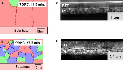
The images on the left-hand side (a and b) display the results of a modeling study of the microstructure evolution of PZT (a) and alkali earth titanates (b) [98]. On the right-hand side, the corresponding SEM micrographs of typical thin film microstructures for PZT and BT films prepared by a hybrid process are shown. (c) The PZT film displays only nucleation at Pt bottom electrode interface (white surface layer is the Pt top electrode). (d) The BT film displays both interface nucleation and nucleation within the bulk of the film, corresponding to a preferred homogeneous nucleation ((c) and (d) reprinted with permission from [82 ] copyright 2004 American Chemical Society)
Although more detailed analyses are possible, only a few concepts are required to use the diagram in Fig. 6 and the basic nucleation and growth equations to interpret film crystallization behavior. These are now listed.
- 1. As crystallization driving force is increased, bulk nucleation becomes (essentially) as probable as interface nucleation. Although the f(θ) term results in a lower energy barrier for interface nucleation, when the crystallization driving force is high, i.e., in typical heat treatment scenarios, there is more than sufficient energy to surmount the energy barriers for all (including less energetically favorable) nucleation events.
- 2. For films that transform with smaller driving forces, the energy barrier heights for different nucleation events are separated to a greater extent. This makes interface nucleation in PZT much more preferred than bulk nucleation, as discussed above, and increases the importance of the substrate in influencing thin film microstructure.
- 3. The effects of crystallization temperature on driving force and nucleation must be considered. When using high heating rates, the physical processes leading to densification and crystallization of the film are delayed to higher temperatures. This causes nucleation to occur at a higher temperature than with conventional heating. Under these conditions, crystallization occurs with lower driving forces, and due to the f(θ) term, lower energy heterogeneous nucleation events become more important.
- 4. Typically, films are crystallized at temperatures well below the melting point of the solid. The importance of processing solution-derived films at these temperatures has been discussed by Wilkinson and co-workers [92].
- 5. Unless rapid thermal processing techniques are used, film crystallization usually begins during heating to the anneal temperature. Therefore, as the temperature of the sample is increased, more thermal energy becomes available to surmount the barriers for nucleation events that are not necessarily the most favorable energetically. This can lead to film microstructures defined by nucleation and growth processes associated with more than one nucleation event.
- 6. The transformation pathway (i.e., the formation of intermediate phases) has a major effect on nucleation and growth behavior, as discussed in the next paragraph.
7.2 Transformation pathways
Two examples will serve to illustrate how different crystallization pathways lead to microstructural variations in perovskite films. We will first compare generally observed differences between PZT and BT thin film microstructures, which are shown in Fig. 7c and d.
These films are representative of those typically prepared at various research institutions [4,5,61,90,100–102]. Most CSD-derived PZT films crystallize with a columnar microstructure with nucleation of the perovskite phase only occurring at the substrate interface [100]. Grain growth from these nuclei proceeds toward the surface of the film through the consumption of a fairly uniform intermediate fluorite (or pyrochlore) phase [103] that is formed after pyrolysis. Because of this type of nucleation and growth behavior, PZT films are usually only a single grain thick. Speck and co-workers have shown that for perovskite materials that transform via such an intermediate metastable phase, the crystallization driving force is reduced by the formation of this phase, resulting in films that display only heterogeneous nucleation at the substrate interface [104]. The specific role of the fluorite phase formation on the orientation selection of PZT thin films has recently been investigated by Norga et al. [105].
In contrast to PZT thin films, BT films are typically non-columnar in nature. This indicates that nucleation within the bulk of the film has occurred, in addition to nucleation at the interface.
From FT/IR spectroscopic investigations [44], it is known that heating of the as-deposited films for some time at an intermediate temperature to remove the organic groups leads to formation of an amorphous film, which is composed of either alkaline earth, carbonate MCO3 (M = Ba, Sr) and titanium dioxide (TiO2), or nanocrystalline M2Ti2O5CO3. Thus, pyrolysis is certainly not complete prior to onset of perovskite crystallization. In addition, fluorite phases are not stable in alkaline earth titanates. Because of the relatively high metastability of the carbonate compounds, as well as the high activation energies of the solid-state reaction between the two compounds, the film must be heated to elevated temperatures to initiate perovskite crystallization. Because the thin film has a homogeneous distribution of the carbonate and oxide phases, the activation energy is nearly the same for all parts of the amorphous film. Once a critical activation energy has been reached, the perovskite phase starts to crystallize. Since crystallization starts at numerous sites with identical surroundings and activation energies, a large number of very small grains is produced throughout the film. The grain size of these films is affected by the formation of an intermediate phase, particularly for certain alkaline earth carboxylates [44].
8 Processing effects and control of thin film microstructure and orientation
8.1 Processing conditions and microstructure
In addition to commonly observed differences between PZT and BT, numerous investigations that have shown that thin film microstructure may be greatly affected by precursor chemistry, deposition conditions and heat treatment schedule. For example, SEM studies of thin film microstructure revealed marked differences for different processing schedules used for BT/ST thin films. These variations are attributed to the different nucleation processes: the two-step pyrolysis and crystallization process leads to very small grain sizes in the polycrystalline thin film [29]; grain sizes are approximately 20–30 nm. In contrast, a larger average grain size is observed for thin films of BT and ST which are pyrolyzed and crystallized with the one-step process in a hot furnace at ~ 750 °C. When the as-deposited film is directly heated to the final firing temperature by inserting the wafer into a preheated furnace, several different processes take place concurrently. After evaporation of the solvent, the organic compounds of the thin film start to decompose. In an ideal chemical surrounding somewhere in the film, the crystallization of the perovskite phase starts at a certain instant at rather low temperatures. Due to the continuous fast heating, the decomposition of the precursors has not yet been completed, although the temperatures are sufficiently high to initiate crystallization. Such a delayed decomposition and crystallization mechanism may cause improved densification due to the high mobility of the elements that is retained to elevated temperature, in accordance with the model of Schwartz [95]. This contributes to grain growth and results in a larger average grain size compared to the pre-pyrolyzed film (two-step method). The increase in the average grain size from 30 nm to 150 nm can have a significant effect on the dielectric properties of the thin films [106].
Some general comments summarizing crystallization behavior are given below.
- • High crystallization temperatures lead to increased densification and larger grains. This is due to the temperature-activated mobility of the ions. Applying concepts of free energy relationships between amorphous and crystalline films, one can further improve the model of the influence of the precursor decomposition temperature on film formation.
- • Stabilization of the Ti alkoxide precursor with chelating agents such as acetylacetone may lead to monomeric species distributed on a molecular scale that show delayed titanium oxide formation. This results in an improved growth mechanism due to the higher mobility of the titanium compound up to high temperatures. This may reduce the number of nuclei leading to a larger average grain size and greater densification. In this case, too, one can apply the model of the free energy relationship mentioned above for the alkaline earth precursor influence to explain the improved thin film properties.
8.2 Control of film orientation
Control of nucleation at the substrate/film interface has been used for the preparation of epitaxial and highly oriented (textured) films. This is particularly important in view of obtaining highly (111)-oriented PZT films on platinized silicon substrates which feature superior switching properties. For films that are subjected to rapid thermal processing, or are processed at higher temperatures, material chemistry, lattice matching with the substrate, and thermal processing parameters are key factors in the preparation of textured or epitaxial films [107–112]. One reason why rapid thermal processing may be beneficial in preparing oriented films is that nucleation is delayed to higher temperatures. Considering the diagram of Fig. 6, nucleation at higher temperatures implies that the crystallization process occurs with a lower driving force. This causes heterogeneous nucleation at the substrate to become more important in defining film microstructure, which may favor the production of films with a higher degree of orientation.
Irrespective of the specific transformation mechanism, to obtain highly oriented or epitaxial films, the film must be processed so that (at the conclusion of processing) heterogeneous nucleation at the interface dictates the microstructure. For the case where only nucleation at the substrate interface occurs, crystallographic growth along fast growth directions (such as in PZT and LiNbO3) can result in highly oriented films; the transformation from the amorphous state to the crystalline state is completely associated with the grains nucleated at the substrate. For other materials, epitaxial films may also be prepared when nucleation occurs both at the substrate and within the bulk of the film. For example, in the processing of yttrium-stabilized cubic zirconia, while epitaxial grains were formed at ~ 400°C, higher heat treatment temperatures were used to densify the film and permit the epitaxial grains to grow and consume the other misoriented grains in the initial polycrystalline film that was formed [107].
The crystal chemistry of the substrate may also play a role in the preparation of oriented films. For substrates that have a higher degree of lattice matching with the film, f(θ) is expected to decrease, which can cause heterogeneous nucleation at the substrate to become more preferred than other nucleation events (see Eqs. (1) and (2)).
Besides effects of the substrate, there have been numerous investigations into the role of the precursor chemistry on both microstructural development and orientation selection [95,113–116]. Various factors have been reported to impact orientation development and different hypotheses have been advanced to explain the observed effects. While some authors [95] have discussed the importance of pyrolysis temperature, others have noted the importance of organic content on the formation of intermetallic layers [117,118]. Recent studies on the growth of PZT on platinized silicon substrates point to a clear influence of precursor chemistry on the orientation selection of these films [119,120]. Fè et al. [119] investigated the evolution of PZT thin films of various compositions prepared from a solution that has synthesized according to a modified Budd and Payne route; instead of 2-methoxyethanol, the less toxic and reactive 2-butoxyethanol was used [31]. These investigators performed a detailed absorption reflection FT/IR analysis of the decomposition products directly obtained from heating the as-deposited film on a platinized silicon substrate to different temperatures and concluded that the chemical structure of the pyrolyzed film has a clear impact on the orientation of the film. Two distinct cases were identified:
- • (1) residual organics in the pyrolyzed film resulted in a strong (111) orientation, while
- • (2) films with large densities of OH bonds prior crystallization exhibit a mixed (111)/(100) orientation.
These authors also extended the above-mentioned model for driving force effects by the assumption of two competing heterogeneous nucleation modes [119].
Whereas in the above mentioned work, the Zr/Ti ratio was varied while the principal precursor chemistry was kept constant, in another study, the precursor chemistry of all employed compounds was systematically changed and the influence on the final morphological and ferroelectric properties was investigated [120]. It was found that even relatively small changes of precursor chemistry, e.g., the use of lead propionate instead of lead acetate, led to a reduction of the Pr values of the ferroelectric hysteresis loops by up to a factor of 50%. The change in precursor chemistry led to a change in the characteristics of the pyrolyzed film, which in turn affected the nucleation and growth behavior, as described in the model above.
The use of chemical solution deposition for the preparation of epitaxial films was first described by Lange and co-workers [107,108] and models for the epitaxial growth of CSD-derived thin films have been proposed by several groups. These are summarized in [121]. Epitaxial grain growth occurs when the film and substrate have identical structures and small lattice mismatch. In contrast, the growth of oriented thin films on substrates with different structure is due to morphological instability phenomena and abnormal grain growth. If the grain size exceeds the film thickness, grains with specific orientations will undergo abnormal grain growth due to their lower surface and interfacial energy. These mechanisms have been studied for ZrO2 thin films on (0001) Al2O3 single crystal substrates that were heated to temperatures between 1200 and 1500 °C [109,122].
Depending on lattice matching and structural differences between the film and substrate the fabrication of epitaxial films proceeds according to four different phenomena.
(1) Epitaxial film growth. For materials that display good lattice matching (difference in lattice constants less than a few percent), the development of epitaxial films involves the growth of small, nanometer-sized grains at the substrate/film interface. The grains eventually grow along the interface and then through the film to consume randomly oriented grains [107,108]. The method has been used for the preparation of epitaxial ZrO2 [110], SrZrO3 [112], PbTiO3 [108], LiNbO3 [123], SrRuO3 [124], and La1–x(Ca,Sr)xMnO3 [125–127]. By optimizing the substrate/CSD-processing relationship, it has even been possible to prepare ultrathin films in the range below 10 nm (Section 10). In case of epitaxial growth relationship between PbTiO3 or SrZrO3, respectively, and SrTiO3 single crystalline substrates, a microstructural instability phenomenon was observed leading to the formation of single-crystal islands instead of continuous films [128,129].
(2) Two-step processing: For the situation where the film and substrate have different structures or large mismatches, the fabrication of epitaxial films is still possible. In this case, epitaxy is achieved through a two-step process where a polycrystalline film is first deposited, and then heated to cause it to break-up into isolated grains (seeds) that possess a low interfacial energy. Subsequently, a thicker layer is deposited onto this surface and the isolated islands act as nucleation sites (seeds) for the growth of a highly oriented film [109]. It should be noted that seed layers have been employed by several investigators for the preparation of highly oriented perovskite films [130–134]; however, in these investigations, it is unclear whether islands are formed in the seed ‘layer’, or if the increase in lattice matching between the seed and the film improves the contact angle and makes nucleation at the seed layer preferred to other nucleation events. Seed layers can also be used to generate a gradient in lattice matching.
(3) Liquid phase processing. When higher processing temperatures are employed, epitaxial films may also form via a liquid phase [135].
(4) One-step processing. Low solute concentrations in the coating solution, when used in conjunction with firing of each individual layer, can emphasize heterogeneous, epitaxial growth and suppress nucleation within the film [85].
Following this approach, it has been shown for two precursor systems deposited on platinized silicon substrates that the multiple coating procedure results in columnar-grained structures if the thickness of each layer is less than 10 nm for BT and less than 20 nm for ST (Fig. 8). Under these conditions, both ST and BT show epitaxial layer-by-layer growth on the underlying perovskite grains. Although the films were deposited at temperatures lower (750 to 800 °C) than those that were typically used in studies concerning grain growth mechanisms, the same models can be applied to these process conditions. Hence, the initializing steps for the columnar growth of the BaTiO3 thin films can be identified as surface instability phenomena and abnormal grain growth, while the columnar structure of the SrTiO3 films is to a large extent initiated by the Pt substrate. This has been observed in TEM cross-section and additional HRTEM studies of the ST/Pt interface [136]. The ST grains exhibit a cube-on-cube relationship with the grains of the Pt substrate layer, which results in a preferred (111)-orientation of the columnar ST film.

SEM micrographs of the cross section and surface of BT and ST films CSD processed from precursor solutions of different concentration ranging from 0.1 M to 0.3 M in a multiple coating process. After depositing each layer a crystallization step has been performed prior to the next coating (One-step process). The corresponding deposited thicknesses per each layer are given in the middle column.
The following examples may serve to demonstrate how knowledge of microstructure control may lead to dense sub-100-nm-thick electronic oxide films, disproving the former assumption that the CSD technique is limited to thicknesses above 100 nm. Films within this thickness regime are normally easier to achieve with gas phase methods, however, it has recently been shown that optimization of precursor chemistry and processing conditions lead to high quality films of thicknesses less than 100 nm. Wouters et al. [137] have optimized a CSD process for PZT, which enabled them to produce dense films of 75 nm with excellent ferroelectric properties. By using the concentration adaptation technique of Hoffmann et al. [85] BST films of 30-nm thickness on Pt-coated Si wafers (Fig. 9) have been prepared. The films are very dense and smooth and show a columnar texture [138].
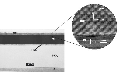
Cross-section TEM image of a BST film of only 30-nm thickness deposited by CSD [139]. The HRTEM (right) shows, by chance, a grain with a [001] orientation. Other grains show similarly clean interfaces but higher indices of the BST film orientation.
The use of these epitaxial relationships (see Section 8) rendered it possible to significantly reduce the thickness of CSD films. For example, in order to build tunnel barriers in colossal magnetoresistance (CMR) oxides, the magnetoresistance (MR) behavior of trilayers consisting of conducting La0.7Sr0.3MnO3 (LSM) and La0.7Ca0.3MnO3 (LCM) electrodes and ultrathin SrTiO3 barriers on a LaAlO3 substrate was studied [139]. It was possible to stack an approximately 5-nm ST film epitaxially between the CMR layers that were approximately 30 nm thick (Fig. 10). This junction exhibits typical tunneling characteristics, such as a temperature independent resistance over a broad temperature range and a strong low-field hysteretic MR. For the LSM stacks, a record room-temperature tunneling magnetoresistance (TMR) sensitivity of 5% at 6 mT was achieved.
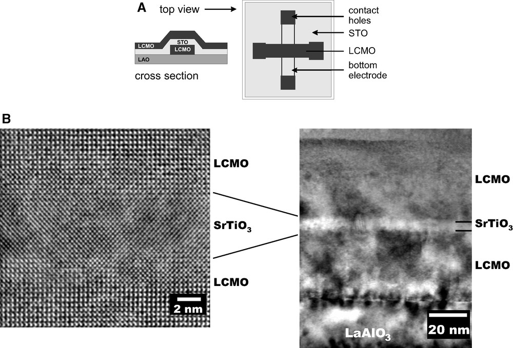
(A) Layout (cross section and top view) of the all-oxide trilayer test structure for determining tunneling magnetoresistance (TMR). An epitaxial stack of 30 nm LCMO/5 nm ST/30 nm LCMO was grown on LaAlO3 by CSD. (B) Overview TEM cross-section photomicrograph showing the complete stack (right) and HRTEM of the magnified tunnel region (left) [139].
9 Low-dimensional nanostructures
The physical properties of materials as they progress from bulk to the sub-100 nm regime continue to be of great interest and increasing importance for future technological applications.
To study scaling effects in ferroelectrics, different CSD based approaches have been applied to fabricate three- and even one-dimensional nano patterned materials.
(1) Alexe et al. used the e-beam direct write technique (EBDW) [140,141] to fabricate regular SBT and PZT structures with lateral sizes less than 100 nm [142,143]. In this approach, a suitable MOD-type precursor solution is first spin-coated onto the substrate followed by drying and local e-beam exposure of the dried gel, rendering the exposed area insoluble in an organic solvent. Subsequently, the pattern is developed by removing the unexposed areas with toluene. Finally, the system is annealed as usual to crystallize the ferroelectric oxide. Using piezoresponse AFM, it was possible to selectively switch the ferroelectric polarization of such structures and to measure their piezoelectric hysteresis loops.
(2) In a kind of self-assembly patterning approach, the above-mentioned microstructural instability phenomenon of very thin PT films on SrTiO3 substrates [128] has been adapted to platinized silicon substrates in a tailored way to generate separated 3-D nanograins [139,144]. Highly diluted PT precursor solutions were deposited onto platinized silicon substrates, subsequently dried, and finally crystallized. Through control of process conditions, notably, the concentration of the initial PT stock solution, different grain size and grain size distributions, ranging from 200 nm to less then 10 nm were obtained at typical crystallization temperatures of 700 °C (Fig. 11). Compared to the above-mentioned single crystalline SrTiO3 substrates, the grain boundaries of the Pt layer decrease the nucleation energy and act as nucleation sites for the perovskite, lowering the necessary temperature. This ‘bottom-up’ method has the particular advantage that damage of the fabricated nanograins, which may occur with other patterning methods like focus ion beam (FIB) or reactive ion etching (RIE), can be avoided. That is the measured physical properties really stem from the material under study and not from other effects like ion implantation. The isolated 3-D nanostructures are studied by three-dimensional piezoresponse force microscopy (PFM) [145]. From PFM investigations it has been found that the smallest grain displaying ferroelectric properties has a size of 20 nm, which possibly marks the limit of ferroelectricity [146]. To fabricate regular patterns of separated ferroelectric nanograins, it has been proposed to first prepare well defined patterns of nanosized TiO2 seeds on different kind of substrates by e-beam lithography/lift-off processing, and subsequently, use these seeds as well defined nucleation sites for the perovskite grains [147,148].
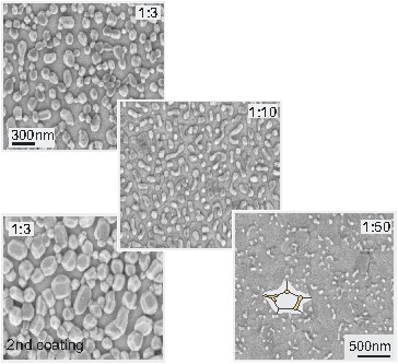
SEM images of PT nanograins deposited onto Pt/TiO2/SiO2/Si substrates displaying the effect of the degree of dilution and impact of a second coating step onto the already deposited and crystallized grains; greater dilution results in smaller the grain size and fewer grains. The inset in the SEM micrograph of the sample derived from the 1:50 diluted precursor solution illustrates the preferred nucleation and growth sites of the grains at the grain boundaries of the platinum film.
(3) One-dimensional ferroelectric nanostructures, such as BaTiO3 nanowires, have recently been successfully prepared by a CSD related method [149,150]. Park et al. accomplished the synthesis of BT and ST nanorods by solution-phase decomposition of bimetallic alkoxide precursors like BaTi[OCH(CH3)2]6 and SrTi[OCH(CH3)2]6 in the presence of coordinating ligands [149,150] at 280 °C. This reaction yields well-isolated nanowires with diameters ranging from 5 to 70 nm and lengths varying from a few hundred nanometers up to tens of micrometers (Fig. 12). XRD, TEM and convergent-beam electron diffraction (CBED) studies of the nanowires give evidence that the nanowires are single-crystalline. The ferroelectric properties of these nanowires have been probed using an ultrahigh vacuum scanning probe microscope with a conductive tip in the electrostatic force microscopy (EFM) mode. These investigations have proven that the BT nanowires are ferroelectric and nearly free of defects.

TEM image of a typical BaTiO3 nanowire with two convergent beam electron diffraction (CBED) patterns shown as insets. The circles represent the region where the CBED patterns are obtained. Analysis of the CBED patterns show that the nanowire is single crystalline with the [001] direction aligned along the wire axis. (Figure from [149] reprinted with permission from Wiley- VCH).
10 Typical applications for CSD processing
Due to the variety of functional properties within the class of complex oxides, the spectrum of applications is huge too. With few exceptions, all types of electronic oxide thin films can be prepared by the CSD technique. Of course, as with every other thin film deposition technique, such as sputtering, evaporation, molecular beam epitaxy (MBE), pulsed laser ablation (PLD), and metallo-organic chemical vapor deposition (MOCVD), CSD has its advantages and disadvantages. Broad overviews of the technologies and the applications are given, for example, in [151–153]. The major advantages of the CSD technique are the relatively low investment costs of the technology and the excellent control of film composition on a molecular level through the control of the stoichiometry of the precursor solution. This includes the opportunity to rapidly develop new CSD routes for the evaluation of new material systems [154] or material systems not previously studied in thin film form (compared to techniques such as MOCVD or MBE). Other advantages are the relative easy fabrication of films over large areas up to multiple square meters for dip and spray coating techniques and the compatibility with standard semiconductor-fabrication methods that offers a high throughput rate (compared to, for example, PLD). The disadvantages of CSD include difficulty in the deposition of epitaxial films and ultrathin films (thicknesses < 30 nm) although the possibility has been demonstrated in selected systems. Another disadvantage of CSD is the fact that 3-D structures with a high aspect ratio cannot be conformally coated.
For applications such as decoupling and filtering on semiconductor chips, packages, and polymer substrates (e.g., embedded passives) allow for planar or low aspect ratio oxide films. These films, with a thickness in the range from approximately 100 nm to 1 μm, are typically prepared by CSD. Adequate high-permittivity materials are BST and BTZ solid solutions. The effective permittivity of these materials shows a dependence on the dc bias voltage, an effect called tunability, which enables varactor devices (voltage dependent capacitors), phase shifters for phased array antennas, as well as tunable resonators and filters for the high-frequency microwave range. On the other hand, there are applications that are hardly accessible for CSD. Integrated capacitors for DRAM node elements require a much higher capacitance density, extremely small lateral dimensions, and 3-D folding. In this case, MOCVD needs to be employed.
Non-volatile ferroelectric random access memories (FeRAM) utilize either PZT derivatives or SBT derivates as ferroelectric oxides. In low memory density FeRAM products, CSD is frequently used as a deposition method. For the high-density 4- or 32-Mbit FeRAM prototypes, CSD is still used by the industry [155] to fabricate the ferroelectric PZT thin film capacitors, although gas phase methods like MOCVD have advantages due to the potential of conformal coverage of small 3-D structures.
Piezoelectric as well as highly electrostrictive functions are frequently realized by ferroelectric thin films typically made of PZT and related materials and often deposited by CSD. These films are integrated into micro-electro-mechanical systems (MEMS) and provide a direct and efficient transformation of mechanical to electric energy and vice versa. Hence, they are useful for various motion and force sensors, linear actuators, micromotors, acoustic and ultrasound devices, electromechanical microwave resonators, microcavity pumps, etc.
The pyroelectric effect of materials is exploited to detect temperature changes with an extremely high sensitivity. The most common devices are uncooled infrared (IR) detectors. Pyrolectric thin films based on perovskite-type complex oxides have been deposited by CSD, to be integrated into 1-D and 2-D arrays for intruder alarms, gas sensors, and IR cameras.
Gas sensors based on surface or bulk resistance effects represent another area in which oxide thin films are usually deposited by CSD. Here, CSD offers the additional advantage, that a specific porosity can be established during the deposition, controlled by the selection of the precursor and the process conditions.
Further classes of devices utilizing the CSD technique are based on, for example, electronically conducting oxides, e.g., SrRuO3, (La,Sr)CoO3, etc. for electrodes or integrated resistors, high-temperature superconductors (HTSC), e.g., YBa2Cu3O7–x (YBCO), magnetoresistive manganates, ferrites, electrochromic oxides, photoelectrochemical systems, and several more.
11 Summary and outlook
This review summarizes the essential developments and foundations of the last two decades in the field of Chemical Solution Deposition (CSD) for high-permittivity, ferroelectric, and other complex electronic oxide thin films. Worldwide research efforts in this field have led to a rapid expansion of the types of material systems that can be prepared, as well as to a tremendous improvement in the quality of the fabricated films. This had led to the preparation of device-quality thin films which are undergoing further development for various applications, and which in selected instances, are in production. This improvement in film quality that has been achieved is at least partially due to the effort that was invested in understanding precursor solution – nucleation & growth – microstructure relationships. In particular, examples of (i) the microstructural evolution of lead-based and barium/strontium-based titanate films as defined by the active nucleation events, respectively, (ii) the formation of ultrathin films, including epitaxial films prepared by CSD, and (iii) tailored bottom-up growth of nano-sized lead based ferroelectric single grains serve to underline the progress that has been made in this field.
Acknowledgements
The authors would like to acknowledge the numerous contributions of their colleagues to the state of the art in this field.