

1 Introduction
Metal chalcogenides (sulfides, selenides, tellurides) are important materials for applications such as photo conducting cells, photovoltaic cells, and other opto-electrical devices [1–5]. Among various sulfides, antimony sulfide (Sb2S3) thin films have gained special attention due to their potential properties such as high refractive index [6] and well-defined quantum size effects [7]. Moreover, Sb2S3 finds applications to the target material of television cameras [8], microwave devices [9], switching devices [10] and in photovoltaic structures [11–14].
Sb2S3 thin films are obtained by various techniques such as vacuum evaporation [15–19], precipitation and sintering [20], the three-temperature method [21], the dip and dry method [22], the solution-gas interface technique [23], spray pyrolysis [24–27], electrodeposition technique [28] and chemical bath deposition technique [29–33]. Among them, chemical deposition method is of a special interest, because this method is proved to be the least expensive, low temperature and a non-polluant method. It is also very suitable for making films of large area.
In order to avoid hydrolytic precipitation of antimony (III) basic salts in aqueous media, one has to work in very acidic solutions, which are inconvenient for film deposition. Another way of avoiding basic salt precipitation is to complex the Sb3+ ion using a suitable complexing agent such as EDTA and tartric acid, and then another chalcogenide source reagent such as thiourea, thioacetamide or selenosulfate.
In this work, the two required precursors were replaced by a single source reagent, namely sodium thiosulfate, which is both a complexing agent for Sb3+ and at the same time a source of sulfide ions upon hydrolysis. The present paper describes the chemical bath deposition of Sb2S3 thin films at deposition time ranging from 10 to 60 min and at different temperature from 40 to 70 °C. The structure, morphology and optical properties of these films were analyzed using X-ray diffraction, atomic force microscopy and UV–vis spectrophotometry.
2 Experiments
The formation of antimony sulfide films can be explained by different mechanisms depending on the dissociation of thiosulfate ions [34]. In our experiment, the chemical bath is weakly acidic (pH = 3.8). The dissociation of thiosulfate ions in acidic solution occurs according to the reaction:
| S2O32− + H+ → S + HSO3− | (1) |
Since the thiosulfate is a reducing agent, it may act as an electron donor and reduce the S to S2−. The thiosulfate forms with antimony ion (Sb2+) a very strong complex Sb2(S2O3)3, which hydrolyses to form Sb2S3 [33] as described by the following chemical reaction:
| Sb2(S2O3)3 + 3H+ + 6e− → Sb2S3 + 3HSO3− | (2) |
or
| 2Sb3+ + 3S2− → Sb2S3 | (3) |
When the ionic product (IP) of Sb3+ and S2− ions produced through reactions in the bath is greater than the solubility product (Ksp = 10−92,77) of Sb2S3 [35], the Sb2S3 film starts deposition at the substrate.
Orange-yellow antimony sulfide thin films were prepared on tin oxide doped with fluorine SnO2:F substrates by chemical bath deposition. The SnO2:F is obtained by spray pyrolysis technique, the composition of the spray solution is:
- • 23 ml of tin chloride, 99%, anhydrous (Acros organics);
- • 5 g of NH4F (puriss p.a., ACS, ≥98%);
- • 7 ml of bi-distilled water;
- • 970 ml of methanol (puriss p.a., ACS).
The SnO2 formed on the surface of the glass substrate heated to the temperature 448 °C, results from the following endothermic reaction:
| SnCl4 + 2H2O → SnO2 + 4HCl | (4) |
The results of optimization of such layers have been reported in previous works [36,37]. The chemical bath for Sb2S3 was prepared in a 100 ml beaker as follows: 650 mg of SbCl3 (puriss. p.a., ACS reagent, ≥99.0%) dissolved in 10 ml of CH3COCH3 (ACS reagent, ≥99.5%). This was followed by the addition of 25 ml of 1 M Na2S2O3 purum p.a., anhydrous, ≥98.0% and 65 ml of bi-distilled water. The SnO2:F/glass substrates were placed vertically into a hermetical closed deposition cell. The chemical bath was heated, the colorless solution turned into orange-yellow at 35 °C indicating initiation of chemical reaction. The thickness of the films is determined by double weight method, using the relation:
In the chemical bath deposition, the deposition thin film was reported to proceed through a nucleation or incubation period followed by a growth phase and terminal phase. Fig. 1 gives the growth nature of Sb2S3 thin films with time period (min). The film thickness increases steadily with dipping time up to 40 min to reach the maximum value of 2.4 μm and the terminal phase in which the growth slows down. The studies were carried out at 40 min and for various bath temperatures varying from 40 to 70°̊C. The obtained layers of Sb2S3 were well homogeneous, uniform and compact.
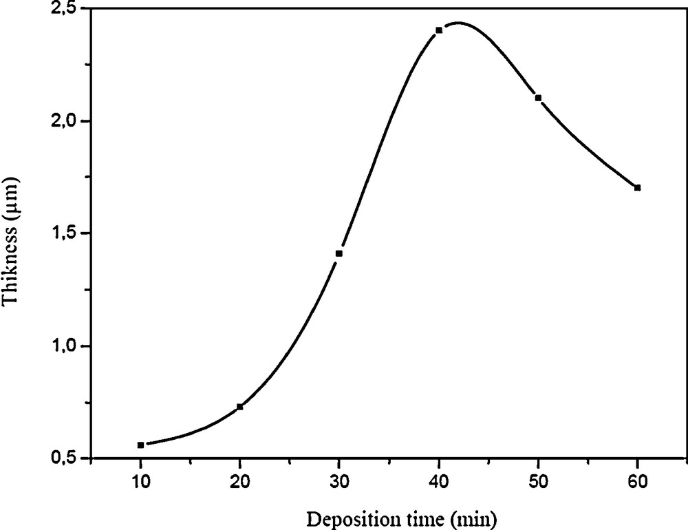
Thickness of Sb2S3 thin films deposited at different time deposition.
The XRD spectra were obtained by means of X’Pert PRO Alpha-1 using CoKα monochromatic radiation and the instrumental broadening is negligible. The wavelength, accelerating voltage and current were 1.789 Å, 40 KV and 20 mA, respectively, with 2θ ranging from 0 to 70°. The scanning electron microscopy (SEM) was carried out with a Quanta 200. Transmittance and reflectance measurements at near normal incidence were performed, at room temperature, over a large spectral range (0.2–2 μm) on Sb2S3 films by a Varian cary 5000 UV–vis/NIR spectrophotometer.
3 Results and discussion
The deposited Sb2S3 films were adherent, uniform, crack-free and covered well over the substrate. The XRD patterns (Fig. 2) of the films deposited at different temperatures in the range of 40 to 70 °C were analyzed. It was found that the Sb2S3 film material is polycrystalline. The labeled peaks in the XRD were compared to the standard JCPDS powder diffraction data set #74-1046 for Sb2S3. The crystallized material is thus identified as orthorhombic Sb2S3. A dominant plane (120) was assigned to the Sb2S3 material at 2θ = 19.10° for films grown at 40, 50 and 60 °C. However, this peak disappears at 70 °C. Peak intensity of the main plane (120) is found to increase from 40 to 50 °C and decrease from 50 to 70 °C until disappearance. Other characteristic peaks (200), (111), (211) and (301) of stibnite structure were present in all X-ray spectra with low arbitrary intensity compared to the (120) peak. We noted also the presence of planes (111) and (210) assigned to the substrate (SnO2/glass). In order to study the grain size of the Sb2S3 thin film particles, films prepared for 40 min at 50 °C, which present a maximum intensity of (120) plane, are studied by taking the slow-scan XRD pattern around the (120) peak. The grain size is estimated using Scherrer's relation:
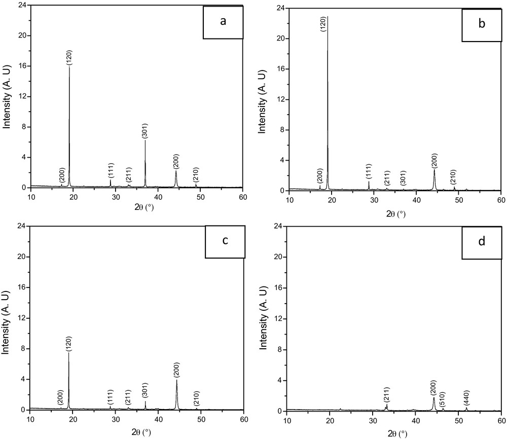
X-ray diffraction patterns of Sb2S3 thin films deposited at 40 min with different deposition temperature. a: 40 °C; b: 50 °C; c: 60 °C and d: 70 °C.
SEM is used for studying the surface morphology of the films. Fig. 3 shows SEM images at ×40,000 and ×10,000 of Sb2S3 film grown at 50 °C for 40 min. In the micrographs, a spherical shape of the grains is obvious in our case as illustrated in Fig. 3. The grains are homogenous and well distributed indicating the formation of uniform thin films. Presence of some irregular distribution of overgrowth of Sb2S3 surface particles are observed in these films (Fig. 3a). Formation of agglomerated surface particles was reported as a common morphological characteristic in Sb2S3 films grown by this method [33,35,38]. The grain size was evaluated from SEM images and the approximate value is around 0.20 μm. The value is greater than the value obtained by XRD analysis. The reason may be that SEM is a tool for surface analysis in the level of micrometers while XRD extracts average information from larger area and entire film thickness.
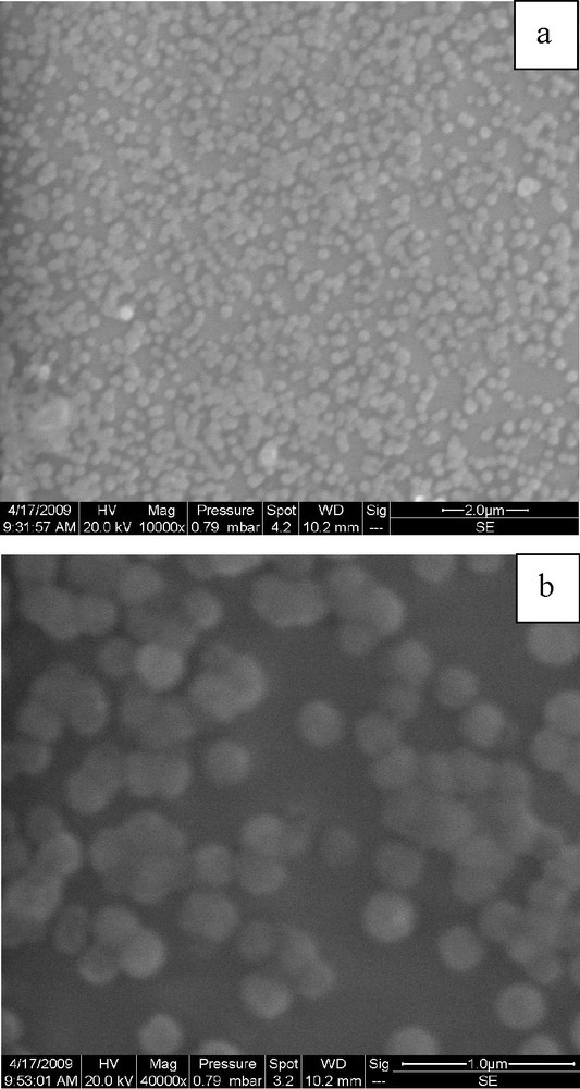
SEM images of Sb2S3 thin film on SnO2/glass substrate. Magnification: a: ×10,000; b: ×40,000.
Fig. 4 shows the optical transmittance and reflectance spectra for a 250 nm thick crystalline antimony sulphide thin film grown on SnO2/glass substrate for 40 min at 50 °C. The broad cut-off of the transmission spectra towards short wavelengths indicates the onset of inter-band absorption in the Sb2S3 layers, while the large wavelengths correspond to absorption edge of the SnO2:(F) underlayer due to the free carries. The corrected transmittance for reflection losses at the air film interface (also displayed in Fig. 4) is calculated using the following equation:
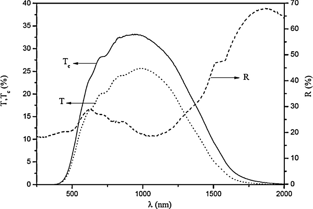
Optical transmittance and reflectance spectra of Sb2S3 film elaborated at 50 °C for 40 min.
Assuming that the reflection is predominantly from the air-film interface where:
In semiconductors, (hαν) is proportional to (hν − Eg)1/n where Eg is the band gap energy and n = 2, 2/3, 1/2 or 1/3 for direct allowed, direct forbidden, indirect allowed or indirect forbidden optical transitions, respectively [39]. Thus, a plot of (hνα)n versus (hν) would yield a linear plot, where the band gap value can be determined from the intercept with the photon energy axis. Concerning crystalline antimony sulphide films, the best straight line fit has been found for values of n = 2, meaning a direct allowed transition between the valence and the conduction band. Thus, Fig. 5 shows plot (hνα)2 versus (hν) for the Sb2S3 thin film grown on SnO2/glass substrate for 40 min at 50 °C. The extrapolation of the data point to the photon energy axis where α2 = 0 illustrates the presence of direct gap located near 2.30 eV for this material. Such a value agrees well with the values of 2.26 eV reported for crystalline Sb2S3 thin films [31], but it is relatively higher than the value of 1.73 eV obtained for samples annealed in nitrogen atmosphere [30,33].
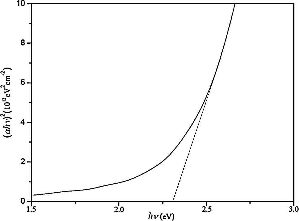
The plot of (αhν)2 versus (hν) for Sb2S3 thin films.
For normal reflectance [40], we have:
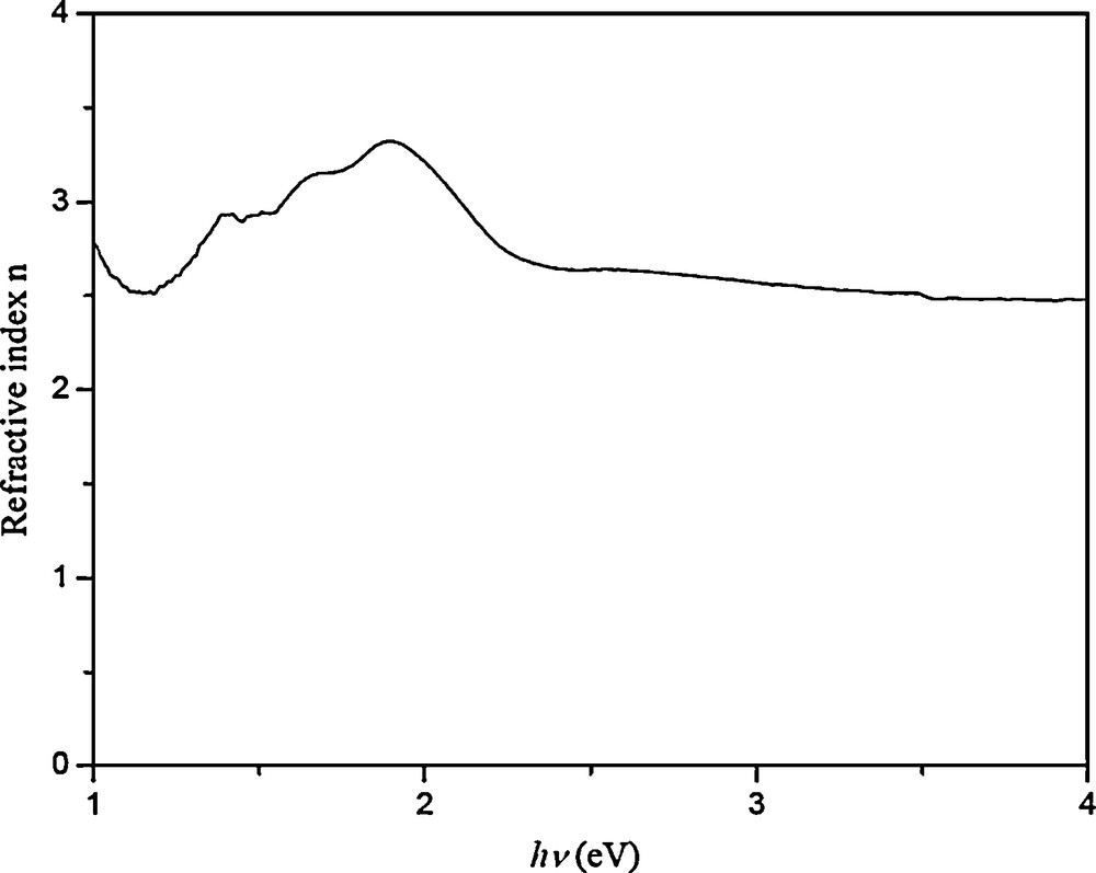
Refractive index versus incident photon energy.
4 Conclusion
A simple chemical method was used for the deposition of Sb2S3 thin films on SnO2/glass substrates. X-ray diffraction studies show that the deposited films at 50 °C for 40 min were well crystallized with the stibnite structure. Scanning electron micrographs show homogenous and well distributed spherical grains indicating the formation of uniform thin films. Optical measurements show that the films present a well-defined direct band gap of about 2.30 eV. The calculated refractive index agrees well with the reported value 2.75. Further work is required to improve the quality of the Sb2S3 films in order to use them as potential materials for the active layer in various solid-state devices, such as thin film solar cells.