


 CC-BY 4.0
1. Introduction
1.1. Background on e-waste challenges
The proliferation of electronic devices is leading to the fastest growing issue of waste management. Concurrently, this need is accompanied by an increasing demand for raw materials for their manufacturing, the extraction of which is also a source of environmental and societal concerns. Furthermore, many raw materials required for electronic device production are exploited only in specific regions of the world, challenging the supply independence of other countries. This is, for example, the case for rare earth elements (REEs: neodymium, yttrium, lanthanum, dysprosium …) [1] or metals like tantalum, cobalt, or nickel, which are fundamental components of many electronic devices [2]. Such metals and materials have therefore been identified as critical raw materials [3].
Facing this dual environmental and strategic challenge, research is committed to developing new solutions for recycling elements found in electronic waste. However, traditional recycling methods fail to recover many such key elements due to their often too low and variable concentration in the overall mass of electronic waste to be processed and the complexity of the associated mixtures of chemical elements. Currently, only about a dozen elements, out of the more than sixty present in electronic waste, are being recycled (see Table 1). Moreover, these traditional recycling methods can potentially be polluting and hazardous because they rely on hydrometallurgical and pyrometallurgical processes [4, 5]. Most of the current recyclers have recycling processes based on these technologies (see Table 1) [6, 7]. The remaining elements are neither recycled nor valorized and mostly end up mixed and diluted in landfilled ashes (bottom and fly), although sometimes used as landfill fill (an application banned in some countries due to the potential leaching of toxic metals by rainwater).
List of some existing recycling processes and elements they can recover, updated from Refs [6, 7]
| Company | Process | Elements recovered |
|---|---|---|
| Umicore | Pyrometallurgy, hydrometallurgy and electrochemistry | Fe, Al, Cu, Ag, Au, Pd, Pt, Ir, Rh, Ru, In, Se, Te, Pb, Sn, Sb, Bi |
| Noranda | Hydrometallurgy and electrochemistry | Fe, Pb, Zn, Cu, Ag, Au, Pd, Pt, Se, Te, Ni |
| Boliden | Pyrometallurgy | Cu, Ag, Au, Pd, Ni, Se, Zn, Pb, Sb, In, Cd |
| DOWA | Pyrometallurgy, hydrometallurgy and electrochemistry | Au, Ag, Cu, In, Pd, Pt, Sn, Pb, Sb, Bi, Se, Te |
| Aurubis | Hydrometallurgy and Pyrometallurgy | Cu, Pb, Sb, Bi, Te, Zn, Sn, Ni |
| Boliden’s Rönnskär | Pyrometallurgy | Cu, Ag, Au, Pd, Ni, Se, Zn, Pb |
| Outotec | Pyrometallurgy | Zn, Cu, Au, Ag, In, Pb, Cd, Ge |
Therefore, today, the primary obstacle to recycling these strategic elements is their low and variable concentrations in the waste stream to be treated. To solve this, it is essential to develop economically viable new strategies for electronic waste management that can simplify the composition and enrich the input materials, allowing us to access these elements and thus reduce the environmental impact of their production while enabling certain regions to access strategic metals that would otherwise be lost.
1.2. Importance of sustainable resource recovery in e-waste management
To achieve this, our analysis of the situation led us to modify the current PCB recycling strategy by combining: (i) a step for disassembling printed circuits, followed by (ii) an advanced component sorting enabling the recovery of targeted elements by the tailored process. The novelty of this approach lies in the technology used for sorting, which, for the first time, allows it to be done based on the elemental composition of the objects to be separated, in order to enrich the outgoing streams with targeted elements [8]. Although various industrial methods already exist for the disassembly phase, which we recently reviewed [9], component sorting is still insufficient, as it is either too rudimentary (done manually), or when optically sorted lacks elemental composition knowledge to sort based on the elements of interest [10]; or too slow (3s per tantalum capacitor recovery using laser desoldering, optical recognition and robotic EC picking) [11]. Two main process families are opposed here: “look and pick” processes, which first evaluate the interesting components on printed circuit boards (PCBs) and then selectively disassemble them, focusing on valuable components, and the “disassemble and sort” strategy, which involves simultaneous disassembly of all components, followed by their sorting, taking into account the total value of the components. Although promising, this sorting strategy based solely on visual recognition quickly reaches its limits when visually similar components have different compositions. Moreover, these approaches are often either too slow or require too much robotic equipment, and hence capital expenditures, to be adopted by a wide majority of recyclers.
To address this problem, several methods for characterizing PCBs and components have been developed and described in the literature. For example, infrared spectroscopy, traditionally used to differentiate plastics, can be applied to the sorting of electronic components [12, 13]. The use of Laser-Induced Breakdown Spectroscopy (LIBS) [14] has also been explored for sorting plastics from electronics, which are often contaminated with flame retardants [15, 16]. These methods can be used to map PCBs and components, creating images in which each pixel represents a spectrum. These hyperspectral images (HSI) contain a large amount of information that can be exploited for component sorting from both spatial and spectral perspectives. However, these methods only allow the analysis of a thin layer at the surface of the component and do not represent the internal composition of materials often encapsulated in plastic, epoxy or ceramics.
To obtain elemental information on the internal composition of often heterogeneous objects, X-ray Transmission Spectroscopy (XRT) at few energy levels (2 to 5 energy bins) has been developed in various fields, mainly in mining, allowing the differentiation of ores through the study of their atomic density [17, 18], as well as in airport luggage scanners. However, this low energy resolution would not allow for the prerequisite capacity to differentiate between chemical elements that are present in PCBs. To address this issue, we present an original method for sorting electronic components that combines optical sorting and multi-energy XRT (MEXRT) relying on artificial intelligence (AI). These new-generation detectors, initially developed at CEA/LETI, have only been commercially available for a few years, under a CEA licensing agreement, from Detection Technologies. Other makers are now also providing such detectors. Indeed, thanks to the 128-level energy resolution of the MEXRT detector used, it is possible to differentiate components based on their elemental composition, hence simplifying the elemental mixture and enrich the final streams with the elements of interest.
This crucial step is highly significant because PCBs exhibit a complex, heterogeneous, and variable composition. Indeed, numerous studies have consistently demonstrated a substantial variation in the composition of different PCBs. Upon careful comparison of these studies, it becomes apparent that, for many elements, the standard deviation for their concentration average can be equal to or even exceed their average concentration (Table 2). Moreover, it should be noted that in some cases, certain element concentrations are not reported from the analysis, either because they were not present or possibly due to the inherent difficulty in quantifying them. Hence, it is worth mentioning that, in the majority of the studies reviewed, refractory elements like Tantalum (Ta) [19], are often not analyzed/reported, the reason is unclear as it is not discussed in these articles. This table highlights the high variability in PCBs composition depending on their type and year of production. Indeed, in most recycling plants, PCBs are received without previous sorting. Therefore, the need for a versatile analytical tool capable of distinguishing and characterizing elements within PCB components is undeniable, as it could play a crucial role in advancing the field of e-waste recycling and critical metals recovery.
Average and standard deviation of metals content in PCBs calculated from analytical values reported in twenty-three different studies [20, 21, 22, 23]; full table and references are available in Supplementary Table S1
| Metal content | Average | Standard Dev. |
|---|---|---|
| Cu (%) | 22.26 | 9.46 |
| Al (%) | 3.67 | 3.32 |
| Pb (%) | 2.50 | 2.70 |
| Zn (%) | 2.51 | 3.58 |
| Ni (%) | 1.99 | 2.89 |
| Fe (%) | 6.41 | 10.42 |
| Sn (%) | 2.61 | 1.48 |
| Sb (%) | 0.06 | 0.01 |
| Cr (%) | 0.18 | 0.25 |
| Na (%) | 0.48 | N/A |
| Ca (%) | 3.05 | 3.30 |
| Ba (%) | 3.05 | N/A∗ |
| Ag (ppm) | 1170.95 | 1570.28 |
| Au (ppm) | 991.50 | 1210.19 |
| Pt (ppm) | 0.00 | N/A∗ |
| Cd (ppm) | 1183.00 | N/A∗ |
| K (ppm) | 180.00 | N/A∗ |
| In (ppm) | 500.00 | N/A∗ |
| Mn (ppm) | 4593.67 | 4836.90 |
| Se (ppm) | 21.00 | N/A∗ |
| As (ppm) | 11.00 | N/A∗ |
| Mg (ppm) | 750.00 | 353.55 |
| Pd (ppm) | 101.00 | 103.41 |
| Co (ppm) | 350.00 | 70.71 |
| Ti (ppm) | 400.00 | N/A∗ |
| Ta (ppm) | 200.00 | 400.00 |
| REEs (ppm) | 30.47 | N/A∗ |
| Total Metals (%) | 32.47 | 7.38 |
∗ N/A indicates that none or only one report of concentration has been found for this element in PCBs.
2. Advanced sorting technics
For the components to be sorted, they first need to be dismantled from the PCBs through a disassembly process. Various industrial or pre-industrial methods are already available for this disassembly, either chemical, by dissolving solder joints using acids, by solder fusion, or by simple mechanical means [1]. These methods all have advantages and drawbacks depending on what constraints are applied to the components, sometimes burning them, corroding them, or possibly breaking them. This is not totally neutral as these alterations can have an impact on the visual aspect of the ECs and therefore on the downstream optical-based sorting process steps and more specifically when it comes to recognizing the components [24]. In our studies, we mostly relied on oven-baking PCBs to melt the solder, followed by vigorous shaking to loosen the ECs and render them free from the bare board.
2.1. Physical sorting process
Although not always efficient as an elemental sorting method, physical methods are simple to use and can easily segregate some similar components [25], and already allow for a simplification of the bin’s elemental composition. Despite the diversity of electronic components, it is important to note that similarities can be observed among components of similar sizes. Therefore, the use of sieve sorting proves to be both easy and effective for removing large components, such as connectors or heat exchangers generally homogenous in terms of composition. Furthermore, this process also eliminates components that are too small for further processing or broken parts of components. This size-based sorting step also contributes to reducing the heterogeneity of the incoming stream by limiting the diversity of components to a few types in each size class, facilitating further sorting processes.
2.2. Presentation of the 10 kg/h sorting prototype
In order to then sort the different electronic components, we chose to convey them on a belt to take them in front of the different cameras, detectors and ejection mechanisms. The prototype has been previously described in detail, and a picture of it can be seen in Figure 1 [26]. In brief, it is composed of a white conveyor belt, measuring 10 cm wide and 2.5 m long, transporting the components under the optical camera and then into the MEXRT spectrometer for classification before they are ejected from the belt into the appropriate sorting bin by a pneumatic air propulsion system.
Picture of the 10 kg/h Electronic Components sorting prototype with (A) the bowl feeder; (B) the Optical camera/Light fixture; (C) the MEXRT housing and imaging system; and (D) Four sorting bins.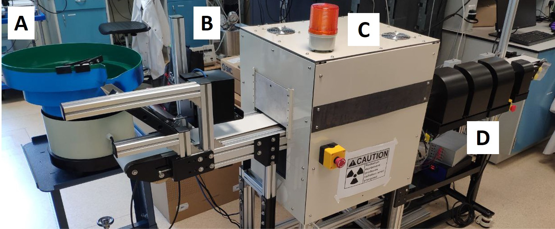
2.2.1. Machine vision-based optical sorting
The components are first subjected to optical sorting. This method utilizes a combination of a high-resolution camera and a convolutional neural network (CNN) specially trained on a dataset created from real components. This optical sorting allows for the precise identification of components by type, leveraging their appearance. With a camera capturing 75 images per second, component image acquisition occurs in real-time. These images are then sent to the computer for classification by the CNN. Optimization of image processing and the recognition algorithm enable the sorting of 60 components per second on a single line with an accuracy above 97%. While this method already separates certain components with relatively homogeneous compositions (CPU, cylindrical aluminum-based capacitors, or copper-rich induction coils), it suffers from a lack of information about the chemical composition of other components, such as resistors, other types of capacitors, or highly integrated electronic components, which are often visually similar but may contain a multitude of different elements.
2.2.2. Multi-energy X-ray transmission spectroscopy
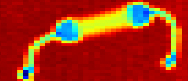
To address this issue of elemental composition-based sorting, components that cannot be differentiated by optical sorting are then subjected to MEXRT sorting. When compared to X-ray Fluorescence (XRF), MEXRT has various advantages. First, since we are looking directly at the absorption of the direct beam, we have the largest possible signal-over-noise-ratio, whereas it is orders of magnitude smaller with XRF when using the same sampling time [27]. Second, we can easily perform an imaging of the devices by combining the 128-pixel 1D detector with the movement of the conveyor belt, which renders a 2D image of the passing ECs. Hence, MEXRT proves to be a rapid method for performing composition-based sorting by using their absorption spectra. Indeed, this method not only relies on studying the atomic density of the material, as a denser material absorbs more radiation at a constant thickness, but also has the ability to study the energy of absorbed radiation. Hence, it is possible to more precisely define the material’s composition by studying the energy of the absorption k-edge of the elements it comprises. The k-edge corresponds to the binding energy of electrons in the k-shell of an atom, representing the minimum energy required for a photon to be fully ejected from this shell. This phenomenon results in a sharp decrease in photon transmission at the corresponding energy, as these photons are absorbed by the electrons. Each chemical element has a unique structure, with binding energies of its core electrons that are specific to it, thus allowing for its identification. By comparing the local maxima of absorption spectra and referencing the theoretical values of these thresholds, it is thus possible to determine the elemental composition of a material from its transmission spectrum (Figure 2).
Schematic description of the dual optical/MEXRT based sorting process.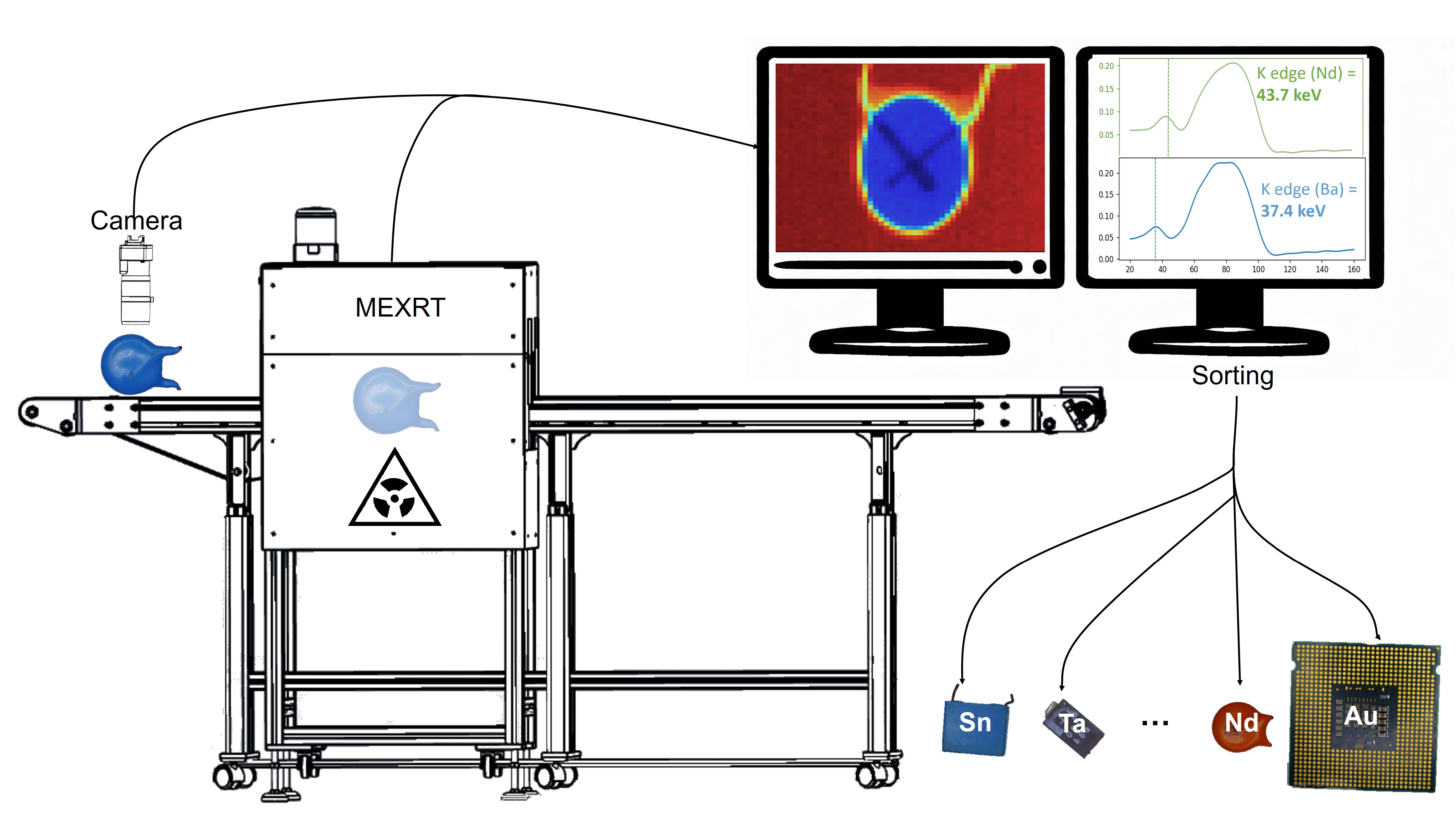
To achieve this, the components are moved on the conveyor belt at a constant speed of 15 cm/s between the X-ray source (VJ X-RAY (NY) LLC MODEL: IXS160BP200P107 equipped with a tungsten anode, working typically at 100 kV and 0.3 mA) and the detector (ME100, Detection Technologies under CEA license). X-rays penetrate the material, and their absorption represents the total radiation absorbed by the elements composing the material. The transmitted radiation is then detected on the other side of the component by the detector. Moreover, the detector used allows for multi-energy spectroscopy. It consists of a line of 128 pixels, with each pixel capable of detecting photons and their energy from 20 keV to 160 keV, with a precision of 1.1 keV (128 levels of energy). By stacking the acquisition lines, it is possible to reconstruct a hyperspectral image of the components, with each pixel representing the transmission spectrum of the material at that specific location. With a pixel size of 0.8 mm and an acquisition speed of 2 ms per line, the image of a 40 mm component can be obtained in 100 ms. Adding the processing time for these hyperspectral images, it is possible to sort up to 4 components per second using MEXRT spectroscopy (and per line of ECs on the conveyor belt). It should indeed be noted that our prototype currently works with a single line of ECs. Faster sorting rates could easily be obtained using multiple lines and an end-of-belt sorting mechanism.
3. Tailored extraction methods and advancements in hydrometallurgical processes
The extraction of electronic components with simplified and specific compositions from the electronic waste stream opens up new possibilities for recycling processes. This is especially relevant when dealing with spent critical metals that are not currently recovered and recycled. This is the case, for example, with the recycling of rare earth elements such as the highly-priced neodymium (Nd) found in ceramic capacitors (according to https://strategicmetalsinvest.com/, its trading price has varied from $65,000 per metric ton in 2020 to $265,000 at its peak in early 2022; it is currently traded around $126,000/Mt). These capacitors use barium titanate (BaTiO3) as a dielectric material, sometimes doped with rare earth elements to adjust its electronic properties. Nd in particular is used in these capacitors, either as a sole rare earth or together with others. From a market share point of view, if Nd is mostly used in permanent magnets, it should be noted that in 2011 capacitors represented 12% of the overall Nd market [4]. PCBs from the urban mine therefore represent a very significant potential source of it. However, no efficient recycling strategy has been proposed nor implemented yet due to its too low concentration in the overall waste PCB supply due to the inaccessibility of a concentrated source of such capacitors. Thanks to the use of our dual optical/MEXRT sorting demonstrator, sorting bins containing almost solely ceramic capacitors containing Nd are now accessible. They can indeed be separated from other electronic components through optical sorting and from visually similar ceramic capacitors using MEXRT sorting with an accuracy of 100% [28]. Using this sorting process, the Nd concentration in the sorting bin containing Nd-containing ceramic capacitors can reach 15% by mass. One can then tailor a specific extraction method based on simple physical and hydrometallurgical processes [28]. In brief, the process begins with a physical beneficiation step involving the controlled fracturing of capacitors, facilitating the separation of their various components through density-based separation and subsequent magnetic sorting. Following this, the fractions rich in Nd are subjected to nitric acid leaching, selectively dissolving the Nd. Subsequently, Nd is precipitated via oxalic acid and ultimately undergoes calcination to yield Nd oxide (Figure 3). This process, tailored for Nd extraction from ceramic capacitors, provides better control over the quantity and reuse of solvents used.
Neodymium (Nd) recovery process from Nd-based ceramic capacitors.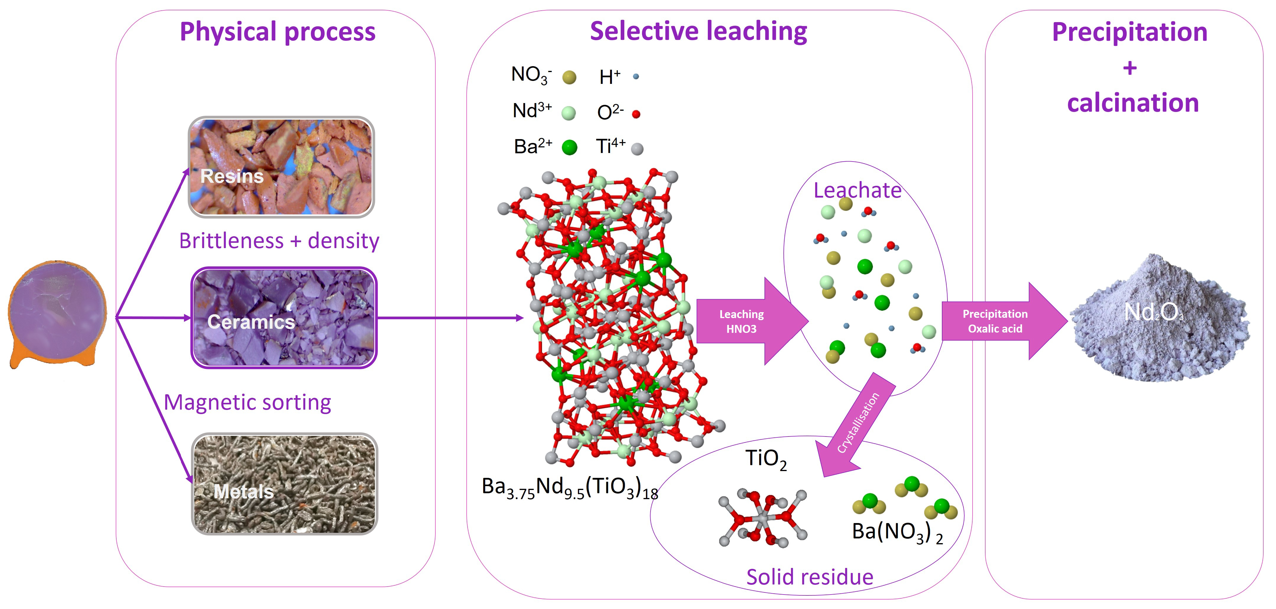
Overall, by combining this sorting with a suitable process for extracting Nd from these capacitors, we modelled that it is possible to establish an economically viable and sustainable recycling process. Indeed, this custom-developed process allows for the recycling of 91.1% of the Nd present in the capacitors into pure Nd oxide at 99.6% purity, and the extra capital expenditure associated with implementing this approach was modelled to be recovered within three to five years (based solely on the Nd recovery) [28]. By developing similar processes or utilizing existing ones for the recycling of other specific components/elements, this sorting method opens up prospects for more sustainable and efficient electronic waste recycling.
4. Large-scale validation and perspectives
The process described in the previous sections based on sieving, optical and MEXRT sorting has then been studied on a larger scale for better evaluation. The performance of this sorting process can be evaluated in two ways: firstly, by its accuracy in sorting components based on a database of known components; secondly, the process’s ability to enrich bins with targeted elements was assessed to study the process’s relevance from this perspective.
4.1. Validation and key figures of the process
Optical sorting allows distinguishing eight types of component families with an accuracy of 97.4%. The use of MEXRT sorting then allows distinguishing other types of components and composition, within any given optical-sorting bin. This is mainly the case for ceramic capacitors, which for example can contain (i) rare earth elements but whose visual appearance provides no information about the composition, or (ii) Ta capacitors. By combining optical sorting and MEXRT, the total process can sort up to fourteen types of components with an average accuracy of 96.9% (Table 3). The global sorting process has been evaluated using a total of 442 ECs divided into different size categories and types (∼50 ECs for each type).
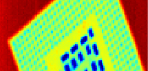
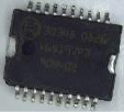
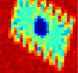
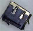
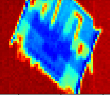
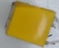
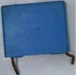
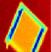
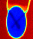
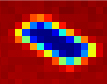
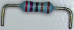
Electronic components with their respective MEXRT images, main elements and recognition precision
| Components | Optical image | X-ray transmission image | Main elements or of interest | Accuracy Global process (optical + MEXRT) |
|---|---|---|---|---|
| CPU |
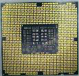 |
 |
Au, Cu | 92% |
| IC chips |
 |
 |
Au, Ni, Cu, Sn, Si | 96% |
| Connectors |
 |
 |
Au, Ni, Cu, Sn, Si | 98% |
| Relays |
 |
 |
Fe, Cu, Sn | 100% |
| Inductors |
 |
 |
Fe, Cu | 100% |
| MPC |
 |
 |
Fe, Cu, Ca, Sn, Al | 100% |
| Al capacitors |
 |
 |
Al, Ni, Sn | 97% |
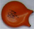
| Nd-based ceramic capacitors |
 |
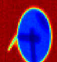 |
Ba, Nd, Ti, Ni, Sn, Ag | 100% |
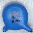
| Ba-based ceramic capacitors |
 |
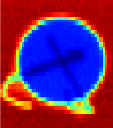 |
Ba, REEs, Ti, Ni, Sn, Ag | 92% |
| Non Ba-based ceramic capacitors |
 |
 |
Ca, Mn, Ni, Sn, Ag | 90% |
| Ta-based capacitor |
 |
 |
Ta, Ni, Mn, Ag, Co, Fe | 100% |
| Ba-based MLCC |
 |
 |
Ba, REEs, Ti, Ni, Sn, Ag | 100% |
| Non Ba-based MLCC |
 |
 |
Ca, Mn, Ni, Sn, Ag | 86% |
| Resistors |
 |
 |
Ni, Cu, Sn | 100% |
Adapted with authorisation from [26].
The speed of optical sorting reaches 60 components per second, while the acquisition and sorting speed by MEXRT is 4 components per second. The average mass of the studied components being 0.65 g, the average sorting speed of the prototype would be 9.36 kg/h if all the components were processed both optically and by MEXRT. Although slower than optical sorting, MEXRT sorting allows for more precise differentiation of other types of components. Due to its reduced speed compared to optical sorting, MEXRT sorting is reserved for a sub-fraction of components that cannot be sorted optically. This dichotomy thus accelerates the overall sorting speed by minimizing the use of MEXRT sorting. Furthermore, it should be noted that this strategy appears reasonable as our current observation is that only 10% of the ECs requires a MEXRT sorting step. Since this step is roughly ten time slower, this indicates that a cascade sorting process for 100% of the ECs is achievable at industrial sorting rates requirements.
Compared to traditional sorting methods, this process combining optical sorting and MEXRT therefore represents a promising solution to meet the needs of electronic waste sorting in the recycling process. This method offers several significant advantages. Firstly, it provides access to a greater number of components, thus expanding the range of recyclable chemical elements. Furthermore, this method allows components to be sorted based on their elemental composition with increased precision. By combining the advantages of fast optical sorting and the capability of MEXRT sorting to differentiate elements, this process represents a major advancement in the field of electronic waste recycling, providing access to classified and chemically simplified components, and enriched in targeted critical elements, once sorted.
4.2. Large-scale sorting evaluation
The process’s ability to sort components and concentrate elements of interest was proven on a larger scale on a mixture of 9.05 kg of waste PCBs [26]. The results of this study demonstrate a significant enrichment of target elements such as Au, Pd, Mn, Ta, or Nd in certain fractions. In particular, sorting CPUs allows for the enrichment of the final stream to a rate of 0.14 wt% in gold, while its concentration was not even detectable in the initial stream (less than 0.1 ppm). Other components, for which recycling processes already exist, were also separated, such as Ta capacitors [24], aluminium electrolytic capacitors [29], Nd ceramic capacitors [28], or multilayer ceramic capacitors (MLCCs) [30]. Although recycling processes for some of these components already existed, a means of accessing them was lacking, and that is precisely what this sorting process now accomplishes and enables.
In addition to its role in enriching streams with certain targeted components and elements, this sorting process also reduces the chemical complexity of sorting bins. Indeed, after sorting, the fraction containing inductors exhibits a composition of 45.6 ± 2 wt% of iron, 38.5 ± 2 wt% of copper, and 20.82 ± 2 wt% of tin. This significant simplification of the composition of the streams greatly facilitates the recycling of various elements, making the streams less complex to process and the recovery rates higher. By eliminating the presence of undesirable elements and enriching the streams with targeted elements, the process contributes to creating more homogeneous streams, thus facilitating their subsequent treatment. Furthermore, the development of microfluidic platforms [31] fully integrated with on-line characterization methods, such as FTIR [32] and XRF [8], will ensure the cost effective and fast development of new hydrometallurgy processes, whether liquid–liquid [33, 34, 35], solid–liquid [36] or for the measurement of thermodynamic data such as components chemical activities, including for the solvent [30, 32].
The larger-scale modeling of this sorting process has demonstrated its effectiveness and relevance for electronic component sorting on Nd-based ceramic capacitors [28]. This process simplifies recycling and access to various elements present in electronic waste by reducing the complexity of the final streams. This approach opens up new prospects for more sustainable electronic waste management and the recycling of previously overlooked and therefore spent chemical elements.
4.3. Perspectives
This prototype enables a sorting speed of 10 kg/h of sorted components on a single line. Extrapolating this technology to an industrial scale enabling 50 components to be classified in parallel, the average sorting speed could reach 500 kg/h. In comparison, plastic sorting lines have a speed comprised between 100 kg/h and 1000 kg/h [37]. In 2020, France generated 849,097 metric tons of electronic waste [38], which translates into ∼23,000 metric tons of electronic components (PCBs represent ∼6 wt% by weight of global electronic waste [39]). With the sorting process presented here, all the electronic components discarded in France could be sorted in 46,000 hours using a 500 kg/h sorting speed. To achieve this task, six 500 kg/h capacity sorting lines would be sufficient to sort all the electronic components generated in France over one year. Extrapolated worldwide (52 Million Mt of waste from electric and electronic equipment), a minimum of ∼725 machines would be needed (with the hypothesis of a 24 h-a-day 365-days-a-year running time). These results suggest considerable market potential for a large-scale usage and application in the field of e-waste recycling. However, collection rates and volumes of e-waste production can vary considerably geographically (from almost 50% at present in the best cases to zero in the worst). For these reasons, different types and sizes of treatment facilities may be needed, whether in the form of large centralized facilities or smaller facilities spread over an area, either in fixed or containerized form, allowing for a nomadic facility that can move to the waste. We are currently expanding our library of economically viable complete processes to as many chemical elements possible (targeting the critical ones first), as well as searching for a tool manufacturer to scale it up and bring it to the market. It should be noted that the output of the developed processes is not only the targeted metals but also allows for the recovery of all the chemical elements in a composition that can be traded. This solution for EC recycling is a paradigm shift in the recycling industry and will require a process upgrade compared to current recycling methods, with the addition of two new upstream process steps (dismantling and sorting). While industrial tools for the first step are already available on the market, we are looking for industrial partners to commercialize this smart sorting tools. The many discussions we have had with recyclers have made it clear that they are eager to have access to this technology.
5. Conclusion
In conclusion, the described prototype and the associated processes, have been validated at a technological readiness level of 4 and they represent a significant advancement in the field of electronic waste recycling. The combination of physical sorting methods, optical characterization, and MEXRT supported by AI allows for the first time to precisely target elements of critical interest to enrich the sorting output streams. This sorting process provides access to strategic and critical elements that were previously lost during recycling processes due to their overall low concentration. Furthermore, this process enables a more environmentally friendly recovery of the targeted elements by tailoring specific process that limits energy and chemicals usage. Finally, this process has been modeled to be economically viable on an industrial scale, thereby opening the door to numerous new business opportunities in the field of electronic waste recycling.
Declaration of AI-assisted technologies in the writing process
During the preparation of this work the authors used “DeepL Write” in order to double-check for English spelling or grammatical errors or typos. After using this tool, the authors reviewed and edited the content as needed and take full responsibility for the content of the publication.
Declaration of interests
The authors do not work for, advise, own shares in, or receive funds from any organization that could benefit from this article, and have declared no affiliations other than their research organizations.
Funding
All authors acknowledge financial support from SCARCE project, which is supported by the National Research Foundation, Singapore, and the National Environment Agency, Singapore under its Closing the Waste Loop R&D Initiative (Award No. USS-IF-2018-4) and Closing the Resource Loop Funding Initiative (Award No. CTRL-2023-1D-01). NMC acknowledges financial support (salary) in 2023 by the REVIWEEE project grant managed by the French National Research Agency (ANR) under the France 2030 program, award No. ANR-22-PERE-0009.