

1 Introduction
Surface nanostructuration, or nanopatterning, is gaining more and more interest in nanotechnology since miniaturizing objects down to the nanoscale can lead to a considerable increase in device efficiency [1]. Pushing feature size and spatial resolution down to sub-100 nm length scales has thus become a priority. Processing of nanopatterned surfaces can be accomplished by “top-down” techniques that consist of creating nanostructures by controlled cutting of supported bulk solids often achieved by selective local chemical etching in lithography, or using powerful (electrons, ions, protons, X-ray) single ultrathin beams (FIB, EBL), offering further possibilities of obtaining complex architectures and high control over pattern regularity [2]. However, the resolution of conventional photolithography is limited by light diffraction through the mask, and single beam techniques encounter the challenges of high fabrication costs, low throughput, and templates lacking durability when the size and periodicity are scaled down [1,3,4].
Alternative approaches that allow fabrication of robust high-resolution nanopatterns over large surfaces are essential for developing technologies compatible with industrial production requirements. A promising alternative that allows overcoming the resolution limitations of lithography is the bottom-up approach. This strategy is based on the self-assembly of molecules or pre-formed nano-objects on the surface such as in the case of block-copolymer self-assembly or nanosphere lithography [5–7]. These strategies have shown great potential in terms of pattern quality and resolution but some issues concerning their processability and their chemical, thermal and mechanical stability are still unsolved. One strong candidate among the bottom-up techniques has emerged recently by the marriage between supramolecular self-assembly, sol-gel chemistry and controlled liquid deposition [8]. The so-called “Inorganic Nanopatterns” (INPs) were obtained by the controlled cooperative self-assembly of inorganic precursors with supramolecular aggregations such as block-copolymer micelles, which can be applied to elaborate 2D materials over large areas.[9] Both structuring and precursor agents are usually dispersed in solution and then applied to a substrate by liquid deposition before curing to stiffen the inorganic phase and eliminate the structuring agent. This strategy allows the facile preparation of large surfaces, patterned with sub 100 nm periodical assemblies, overcoming the scale-up and resolution limits of most lithographic methods. Once deposited onto a substrate, these inorganic nanopatterns (INPs), bearing periodic physical and/or chemical heterogeneities, can be exploited in many applications. The present article reviews the preparation of such INPs based on TiO2, ZrO2, and CaTiO3, and how they have been exploited in nanofabrication or as a functional component for different domains of nanotechnology as illustrated in Scheme 1. In this contribution, we will first describe how this novel generation of substrates is prepared and how one can perfectly control the morphology and the dimensions of the nanoperforation motifs. Some examples of how the ordered topography can be used to add new functionalities to the system will be shown. In particular, they have been used as controlled wetting surfaces, as photoactive layers, as growth directing substrates for co-deposition of magnetic, semiconducting, photomagnetic, and photoluminescent dots…, as nanoelectrode arrays, as charge injection and recombination enhancers in HyLed stacks. In addition, they have been combined with nanofabrication techniques such as reactive ion etching and deep X-ray lithography for the fabrication of even more complex nanostructures.
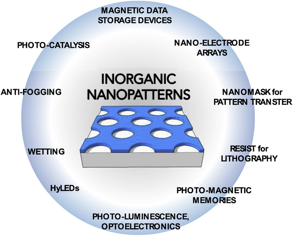
Domains of applications of sol-gel derived inorganic nanopatterns.
2 Controlled elaboration of inorganic nanopatterns
2.1 Overview of the chemical/process strategy
Metal oxide inorganic nanopatterns were synthesized via a sol-gel based strategy based on the co-deposition by dip-coating of the inorganic precursors and block copolymer micelles, followed by a short thermal treatment. [9] INPs can be made from almost any inorganic precursors, giving rise to a wide panorama of compositions, taking advantage of the versatility of sol-gel chemistry. In the following sections we will discuss the case of titania, calcium titanate, and zirconia nanopatterns prepared with commercial polybutadiene-polyethylene oxide block-copolymers. Compared to others, this type of block-copolymer has been chosen because it forms micelles in the typical ethanol/water system and it usually does not require other unfriendly solvents, such as THF or dichloromethane, to adjust the medium polarity [10].
The overview of the typical INP preparation steps is illustrated in Fig. 1. This protocol was followed for each of the prepared systems. Synthesis conditions and structural characteristics are reported in Tables 1 and 2. First, (a) the PB-PEO templating agent is mixed with water and with ≈ 4/5 of the total amount of ethanol. (b) The solution is annealed at 70 °C for 2–4 h until complete dissolution of the block copolymer. During cooling down at room temperature, homogeneous spherical micelles form with the hydrophobic PB chains comprising the core and the hydrophilic flexible PEO shell been in interaction with the relatively polar solvent. (c) The chloride salt precursors are then dissolved in the remaining ≈ 1/5 part of ethanol. Both inorganic and block copolymer solutions are then mixed together. The Ti(IV) and Zr(IV) species are expected to remain in the PEO-hydro-alcoholic medium shell since the polar PEO units are hydrophilic and have the ability to form strong coordination bonds with the M (IV) metallic center through the interaction between the free electron pairs of O atoms and the vacant d-orbital of the metallic atoms (Lewis acid / base pair). (d) After mixing the system for at least 2 h, the substrate is dip coated in the solution. Through the exact control of the deposited material, the surface is covered just by a monolayer of micelles surrounded by the inorganic species. (e) The final step is the thermal treatment that enables the complete evaporation of the absorbed water, the decomposition of the block-copolymer, and eventually the condensation and potential crystallization of the oxide matrix.
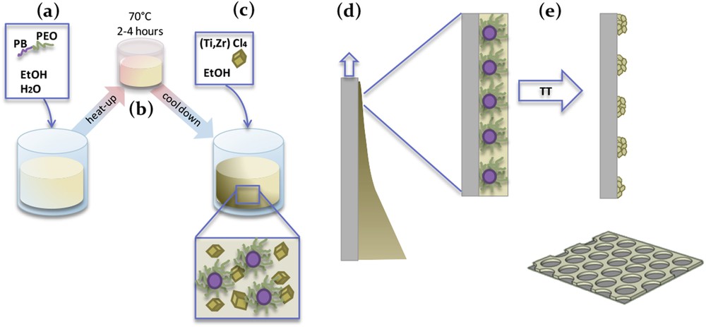
Schematic illustration of the preparation process of inorganic nanopatterns.
Chemical and process parameters used to fabricate the ZrO2 INP.
| Structure | Solution compositions | Processing conditions | ||||||
| D nm | b nm | PB-PEO | m | c mmol/L | u mm/s | T Dipcoating | TT 5 min | |
| A | 9 | 15 | 8678 | 1.5 | 38.3 | 0.5 | 25–40°C | 500°C |
| B | 12 | 25 | 6605 | 1.5 | 38.3 | 0.5 | 25–40°C | 500°C |
| C | 14 | 40 | 3902 | 1.1 | 33.9 | 1.2 | 25–40°C | 500°C |
| D | 16 | 26 | 2753 | 1.5 | 38.3 | 0.5 | 40°C | 500°C |
| E | 17 | 34 | 3017 | 0.8 | 68.2 | 0.5 | 40°C | 500°C |
| F | 18 | 36 | 4755 | 1.5 | 34.1 | 0.5 | 40°C | 500°C |
| G | 17 | 44 | 3017 | 6 | 11.4 | 0.5 | 40°C | 500°C |
| H | 20 | 41 | 3017 | 3 | 22.7 | 0.5 | 40°C | 500°C |
| I | 24 | 35 | 3017 | 1.5 | 34.1 | 0.5 | 40°C | 500°C |
| L | 25 | 64 | 1945 | 1.5 | 50.3 | 1.2 | 60°C | 500°C |
| M | 32 | 42 | 2999 | 1.5 | 50.3 | 0.5 | 25–40°C | 500°C |
| N | 31 | 89 | 2231 | 1.5 | 49.1 | 1.2 | 40–60°C | 500°C |
| O | 42 | 75 | 3397 | 0.7 | 76.6 | 1.5 | 60°C | 500°C |
| P | 51 | 79 | 3397 | 1.5 | 38.3 | 1.5 | 60°C | 500°C |
| Q | 53 | 81 | 3397 | 3 | 19.2 | 1.5 | 60°C | 500°C |
| R | 67 | 110 | 2325 | 1.5 | 34.1 | 2.5 | 60°C | 500°C |
Chemical and process parameters used to fabricate the TiO2 INP.
| Structure | Solution compositions | Processing conditions | ||||||
| D nm | b nm | PB-PEO | m | C mmol/L | u mm/s | T Dipcoating | TT 5 min | |
| A | 9 | 16 | 8678 | 1.8 | 26.7 | 0.5 | 25–40°C | 500°C |
| B | 15 | 39 | 3902 | 1.8 | 37.5 | 0.5 | 25–40°C | 500°C |
| C | 17 | 33 | 2753 | 1.8 | 26.7 | 0.5 | 25–40°C | 500°C |
| D | 17 | 47 | 3017 | 10 | 5.75 | 0.5 | 25–40°C | 500°C |
| E | 20 | 42.7 | 3017 | 4 | 12.3 | 0.5 | 25–40°C | 500°C |
| F | 27 | 39 | 3017 | 1.8 | 21.5 | 0.5 | 25–40°C | 500°C |
| G | 29 | 43 | 2999 | 1.8 | 25 | 0.9 | 25–40°C | 500°C |
| H | 28 | 68 | 1945 | 1.8 | 28.1 | 0.9 | 40°C | 500°C |
| I | 28 | 72 | 2231 | 1.8 | 36.8 | 1.2 | 40°C | 500°C |
| L | 42 | 88 | 2325 | 0.8 | 56.6 | 1.2 | 40–60°C | 500°C |
| M | 48 | 95 | 3397 | 1.8 | 35.1 | 1.5 | 25–40°C | 500°C |
| N | 58 | 98 | 2325 | 1.8 | 24.2 | 3 | 40–60°C | 500°C |
An example of titania INPs on a silicon substrate is shown in Fig. 2. The SEM-FEG images display the characteristic nanoperforations of about 20 nm in diameter. Several domains with hexagonal-type compact structure and of a few hundreds of nanometers long-range ordering are found with different orientations. Fig. 2(b) shows the SEM-FEG photo of the cross-section tilted at 70°; one can clearly identify the perforation network, and the good adhesion to the silicon substrate. The same surface has been characterized by X-ray diffraction and the corresponding GISAXS 2D pattern is displayed in Fig. 2(c). The organization of the perforations into a 2D hexagonal-like structure leads to the presence of the two characteristic diffraction rods indexed (100) and their harmonics. The elongated shape of the rods suggests that the film is very thin and the perforations have a low aspect ratio. Their elongation in the vertical direction (normal to the surface) evidences that a single layer of nanoperforations is present with a similar trend on the whole irradiated surface. The intensity profile in the qy direction, reported with the blue line, shows a d-spacing of 33 nm that corresponds to the (10) planes. This morphology is confirmed by atomic force microscopy (AFM), as reported in Fig. 2(e). Spectroscopic ellipsometry can also be used to determine the thickness of the layer as a function of the process conditions and to follow the evolution of the thickness upon thermal treatment by in-situ ellipsometric analysis. The combination between all these techniques gives access to a complete structural characterization of the INPs, throughout the determination of the following values:
- • D – average diameter
- • b – center to center distance
- • w – wall thickness –
- • d(10) –
- • h – thickness

Titania nanoperforated thin film: (a) SEM-FEG top view and autocorrelation function in the inset; (b) 70° tilted SEM-FEG micrograph; (c) the GI-SAXS pattern and intensity profile in the blue line; (d) structural parameters of the array; (e) surface topography by AFM.
The adjustment of these structural characteristics is achieved through a precise tuning of the solution chemical composition and of the conditions of liquid solution processing. In what follows, we will discuss the influence of each of the following critical parameters (Mn+ stands for the sum of all inorganic cations used as precursors).
- • B – Units of butadiene in the PB chain
- • EO – Units of ethylene Oxide in the PEO chain
- • – Molar concentration of EO in ethanol
- • – Molar ratio between the metal salt and the PEO
- • – Molar concentration of the inorganic salt in ethanol
- • – Molar ratio water/ethanol; 0.11 for TiO2; 0.17 for ZrO2
2.2 Influence of the block copolymer chain lengths
The easiest and more effective way to tune the size of the holes and their center-to-center distance is to choose the suitable structuring agent as shown in Fig. 3. Several ZrO2 INPs have been prepared from PB-PEO block copolymer micelles having a wide range of lengths of both PB and PEO chains. For all the samples, the ratio m (the molar ratio between the metal salt and the PEO) was fixed constant at 1.5. Fig. 3(a) shows the correlation between the units' number of Butadiene (B) and the average perforations size D. Similarly, the wall thickness (w = b−D) versus the length of the ethylene-oxide chain (EO) is plotted in the graph of Fig. 3(b). The plots in Fig. 3 evidence a fairly good linear relation between the PB chain and the average final diameter and the PEO chain with the wall thickness respectively. INPs prepared using different PB-PEOs are shown in the SEM images (Fig. 3(c–f)). As expected, longer PB-PEO chains lead to larger micelles, and therefore to larger perforations. In this way, the center to center distance b of the INPs can be easily adjusted between 15 nm and 110 nm.
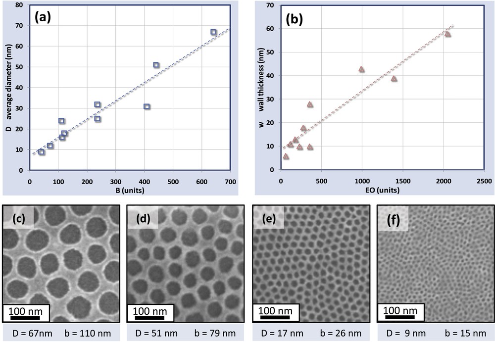
Correlation between the PB-PEO chain and the structural parameters D and W of the ZrO2 nanoperforated layers. (a) Plots of the average diameter versus chain length of butadiene. (b) Plots of the wall thickness versus the chain length of ethylene oxide. (c), (d), (e) and (f) SEM micrographs of ZrO2 obtained from typical block-copolymer micelles with different chain lengths.
2.3 Influence of the inorganic precursor to block copolymer ratio
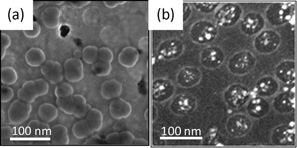
Another parameter that has been taken into account is the molar ratio m between the metallic precursor and the ethylene oxide in the template. Evidence of the latter consideration is reported in Fig. 4. For this investigation, a highly diluted solution of c = 12.2 mM was used to deposit dispersed hybrid micelles instead of a continuous network. Under these conditions, and fixing m = 2, arrays of TiO2 nanorings were obtained. The AFM topography of the surface bearing discrete single rings is displayed in Fig. 4(a), while the depth profile from the ring center to the outer part is plotted in Fig. 4(b). Three regions can be identified: region 1 is the internal hole of the ring (average diameter of 65 nm) and corresponds to the PB core of the initial micelle; region 2 is the thicker corona referring to the polar EO part of the micelle. Assuming that the coordination of Mn+ by the EO groups is highly favorable, most cations are prevalently located in region 2 for m ≤ 1. In the case of Fig. 4, the molar ratio Ti4+/EO is equal to 2 (m = 2). There is an excess of cations that cannot be coordinated and is free in solution and is found in the outer part of the ring after deposition in region 3. Other ring systems have been obtained starting from solutions having different m ratios (from 1 to 8). For each system we considered 20 rings and the depth profile (from the center to the outer part of the ring) was accessed by AFM for each of them. The average depth value was plotted for each system versus the distance from the center of the ring in Fig. 4(c).
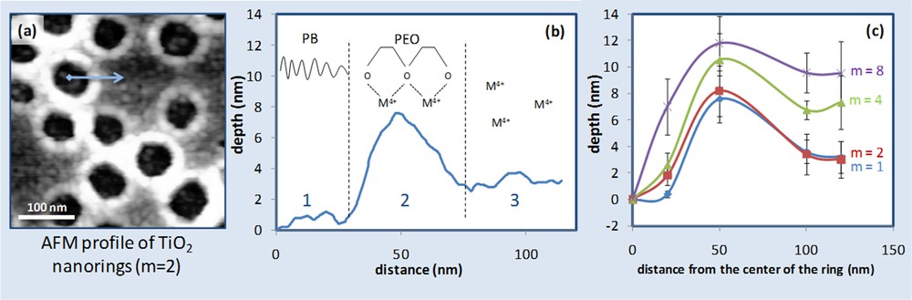
(a) AFM topography of TiO2 nanoring arrays; (b) depth profile versus distance from the ring center; (c) evolution of the depth values at distances ranging from 0 to 120 nm from the center for various m values (m = Ti4+/EO).
As expected, this results in an increase of the thickness of the rings for higher values of m. The latter consideration is more evident in region 3 where, for m = 8, the outer part of the ring has almost the same depth as that of the corona. Additionally, for higher m, the corona is broader, suggesting also a reduction of the perforation diameter (error bars are related to the sharpness of the AFM tip). The influence of the parameter m on INPs prepared from more concentrated solutions, for which a continuous network can be described, is shown in Fig. 5. Three films were obtained from 3 starting solutions having Ti4+/EO molar ratios equal to 1.8, 4 and 10. Solutions with higher m (and thus richer in Ti4+) have been diluted in order to keep the same inorganic content (see Table 2 preparation d–f). SEM photos of the samples are reported in Fig. 5 (a–c). Samples obtained by solutions having m = 10 exhibit perforations assembled in pseudo-squared arrays that is an indication of the formation of a bi-layer system. The micrographs have been image-analyzed and the resultant values of D, b and % area covered are reported in Table (h) in Fig. 5.
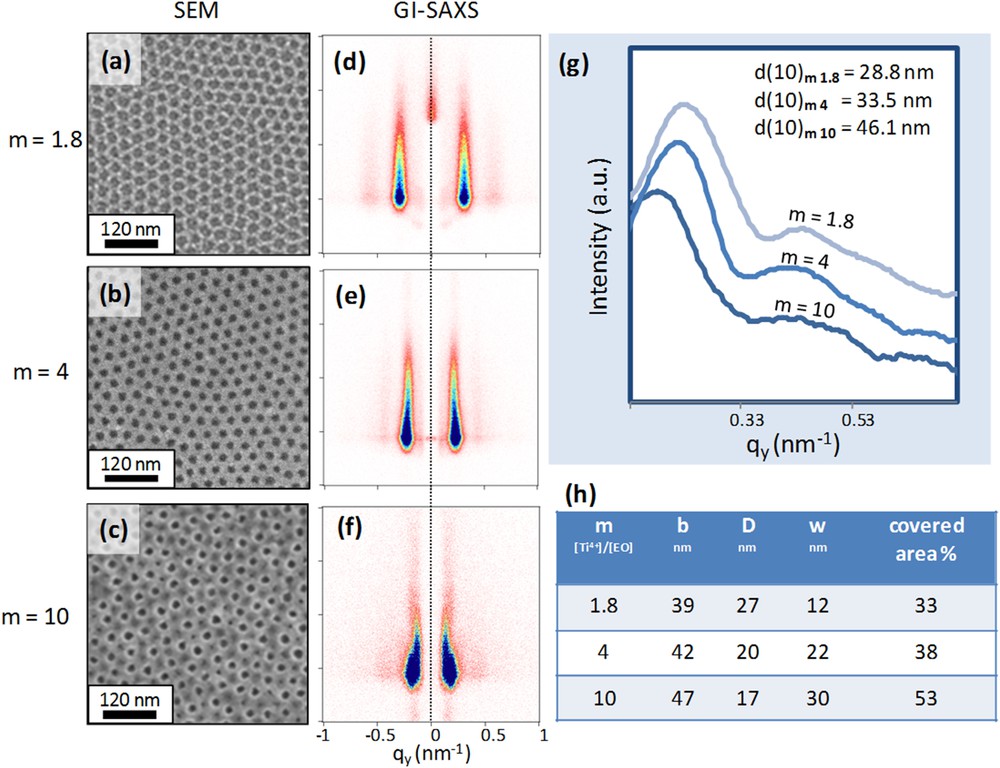
Nanoperforated layers obtained from solutions having m equal to 1.8, 4 and 10. SEM photos (a), (b), (c) and GI-SAXS patterns (d), (e), (f) respectively; (g) plot of diffraction intensity versus qy; Table (h) gathering structural parameters obtained from image analysis.
As expected, the area covered by TiO2, and the center-to-center distance, both increase when increasing the ratio m, which consequently leads to a lower density of perforation and smaller perforation size. The periodicity of the three layers has been accessed by GI-SAXS and the corresponding 2D patterns are shown in Fig. 5 (d–f). The plots of the diffraction intensity versus qy for the three INPs are shown in Fig. 5(g). The (10) diffraction rods shift to lower qy values for increasing m ratio, confirming the microscopy analyses.
2.4 Solution conditioning to improve micellar homogeneity
As described in Fig. 1, step (b) consists of heating the solution containing the block-copolymer at 70 °C for 2–4 h until complete dissolution. Cooling triggers the self-assembly of BCP into micelles through a progressive decrease of solubility. The rate of cooling has an influence on the rate of micellization and therefore on the distribution in size of the micelles and consequently on the final perforation homogeneity. A qualitative indication of such a kinetically driven effect is shown in Fig. 6. Two identical initial BCP solutions (free inorganic precursors) were heated up at 70 °C for 2 h. The first one (i) was rapidly cooled down at 20 °C with a rate of −5 °C/min. The second one (ii) was taken back to room temperature at a rate of – 1 °C/min. Inorganic precursors were then added to both solutions just before INP elaboration. The SEM photos of the resulted INP are shown in Fig. 6 (i) and (ii) with the respective autocorrelation functions in the insets. A broad size distribution of the perforations and a poor organization resulted from the rapid cooling-down process. On the other hand, the film obtained from slow cooling-down exhibited a narrower perforation size distribution (Fig. 6b), which leads to a higher degree of hexagonal organization. The SEM photo in Fig. 6 (ii) highlights with the dashed lines the presence of quasi-perfectly organized domains having sizes of 400– 500 nm. Due to the length of co-polymer molecules and of the related entropic factor, a slow micellization is needed to achieve the thermodynamic homogeneous distribution through the slow dynamic exchange. This is further confirmed by the fact that a several-day long ageing of the micellar solution (>5 days) before adding the precursor leads to even narrower size distribution. This is probably one of the main important criteria to follow to improve the degree of local organization and the long-range ordering of the patterns. The assembly takes place during the evaporation and consists of the arrangement of the micelles that are considered as rigid spheres. The homogeneity in the size of these spheres is a necessary condition to obtain highly organized motifs such as in the case of colloidal lithography [11]. Other self-assembled systems such as pure block-copolymer thin films can be annealed after deposition at high temperature or in a saturated solvent atmosphere in order to increase the chain mobility and improve long-range order arrays [12]. This is not the case for most sol-gel systems since after evaporation of the solvents, cross-linking of the inorganic network takes places, provoking a consequent loss of mobility.
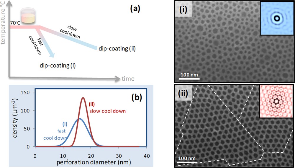
(a). Schematic diagram of the cooling down and ageing steps. (b) perforation size distribution for the two samples; ZrO2 layers on Si after fast cooling down (i) and after slow cooling down and ageing (ii).
2.5 Mastering dip-coating processing conditions for INPs
Sol-gel layers can be obtained by liquid deposition processes such as spin coating, dip coating, dropcasting, etc. Despite the fact that these techniques are well known and easy to apply, the deposition and, eventually the self-assembly of the preformed micelles, is a complex multi-step mechanism that involves homogeneous wetting of the substrate, evaporation of the volatile species, and dynamic evolution of the physico-chemical characteristics (concentration, viscosity, solvent polarity, temperature). The combined effects of all evaporation-governing parameters can be controlled and contribute to the quality of the layer in terms of thickness, nano-ordering, and long-range homogeneity. Dip coating is without any doubt the technique that allows the highest degree of control during evaporation and can be applied to large surfaces without wasting the mother solution [13]. A good control on withdrawal speed during the process is necessary to prepare perfectly homogenous or controlled graded films [14,15]. The process thus plays a key role in the formation of good quality INPs since they are formed by a single monolayer of micelles and the quantity of material applied has to be carefully modulated. A higher film thickness leads to multilayers of micelles and thus to a mesoporous film (if not collapsed after thermal treatment). A lower amount of materials applied on the substrate will result in an uncompleted covering of the surface with the formation of islands of nanorings as shown in the AFM micrograph of Figs. 4(a) and 7(c).
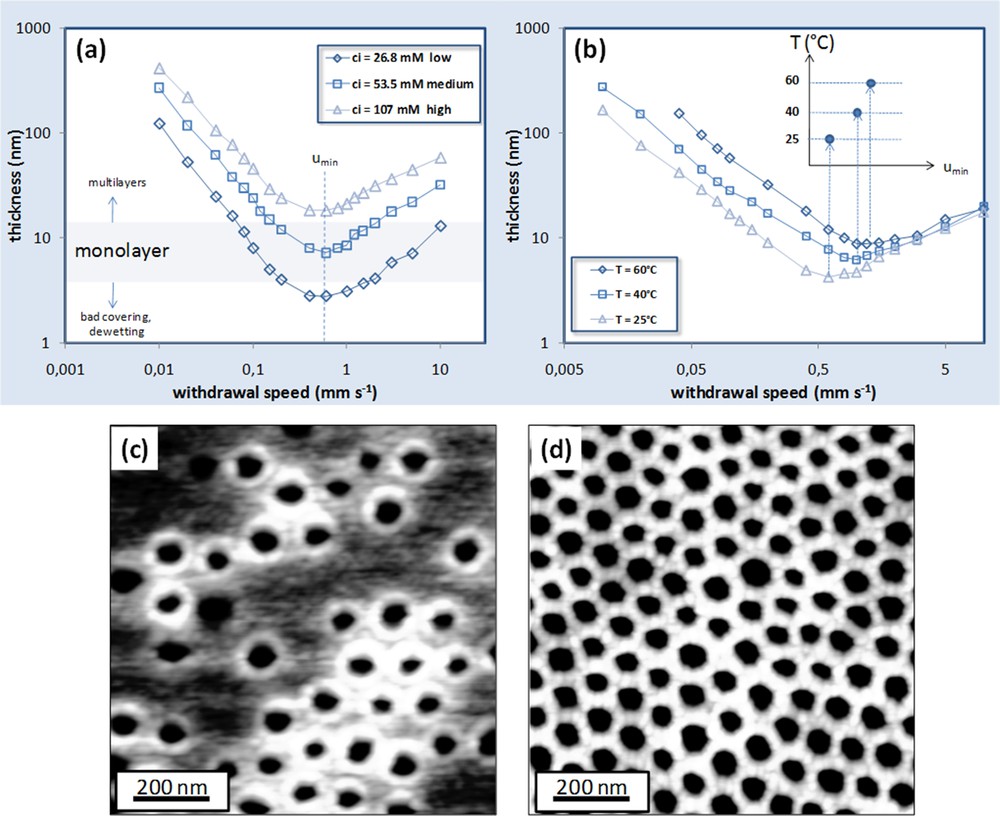
Final thicknesses versus withdrawal speed for a PB-PEO titania system. (a) The influence of concentration of the inorganic part and (b) the influence of the evaporation temperature. AFM micrographs showing (c) low coverage of the substrate (nanorings) and (d) monolayer of nanoperforations.
Fig. 7(a) shows the plot of the final thickness versus withdrawal rate at 25 °C of a TiO2 system for three different inorganic molar concentrations ci (called low, medium and high) with the ratio Ti4+/EO m = 2. The typical tendencies attributed to the capillarity and draining regimes are highlighted for low and high withdrawal speeds respectively [13]. As expected, the more concentrated solutions lead to thicker final films. For intermediate speed, a minimal value of thickness is found for each concentration that is referred to as critical speed uc equal to 0.7 mm·s−1 in the three cases. For the preparation of good quality perforated layers, the final thickness must be found between 7 and 15 nm. INPs can be obtained from the “medium” concentration in a wide range of speeds, corresponding to the mixed regime. If the more concentrated solution “high” is used, multilayers of micelles are always obtained even dipping at critical speed uc. The dip coating in dry air at high temperature often results in a better quality of the patterns since a higher evaporation rate prevents dewetting and leads to more homogenous layers. The evaporation temperature in the chamber was thus investigated in detail. Fig. 7(b) shows the plot of the final thickness versus the withdrawal speed for the “medium” concentrated solution deposited at different temperatures inside the chamber (25, 40, 60 °C). As reported in previous studies [13], the temperature in the chamber affects the final thickness only for low withdrawal speeds, because the capillary deposition is governed by the evaporation rate of the solution in the meniscus region. On the other hand, in the draining regime, the evaporation rate does not influence considerably the final thickness.
The increase of the evaporation rate induces an increase of the minimal thickness and a shift of the corresponding critical speed uc to higher values. From the same “medium” concentrated solution, good quality mesoporous films can be obtained at lower withdrawal speed as shown in Fig. 8. The TiO2 layer obtained in the capillarity regime (u = 0.1 mm·s−1 at 60 °C) is 90 nm thick and is mesoporous with a 3D ordered organization of pores.
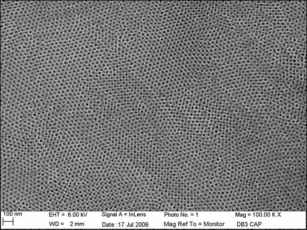
SEM image of the surface of a PB-PEO templated titania film, obtained in the capillarity regime and after thermal treatment at 500 °C.
2.6 Thermal treatment step
The evolution of the thickness of a PB-PEO templated ZrO2 system with temperature has been accessed through thermal ellipsometric analysis (TEA) as displayed in Fig. 9. The experiment consists of an in-situ measurement of the thickness and refractive index by spectroscopic ellipsometry while the sample is heated. In the presented example, the sample was heated with a continuous ramp rate of 10 °C per min. Curves of thickness h and its derivative dh/dT versus temperature allow identification of the phenomena occurring during the thermal treatment. Between 25 and 100 °C, a significant contraction occurs due to desorption of water and ethanol. After 100 °C the thickness contraction is less pronounced: the system starts to consolidate due to the polycondensation reactions and the consequent formation of the rigid inorganic network. Around 200 °C the highest contraction occurs due to the decomposition of the block-copolymer. At 380 °C a slight decrease of thickness and the simultaneous increase of refractive index (not shown) are attributed to the crystallization of the tetragonal zirconia, as also confirmed by X-ray diffraction analysis (data not shown). After crystallization, diffusive sintering takes place, inducing complete opening of the perforations. Further heating-up is accompanied by Ostwald's ripening of the elementary particles that eventually results in solid dewetting. Particles would then discretize and grow in height, as suggested by the increase of the thickness at temperatures higher than 600 °C. Different from the TEA ramp, in the standard preparation of the INP, the layers are treated by flash thermal treatment at 500 °C for at least 5 min. According to the literature [16], in the case of faster heat treatment, the block-copolymer decomposition and crystallization temperatures are expected to be shifted to higher values. One example is shown in Fig. 10 for TiO2 INPs heated up directly to 300, 400, 500 and 600 °C for 5 min. After calcinations at 300 °C we can barely distinguish the sites where the micelles were assembled before being decomposed. After 5 min at 400 °C the system is evolving but the perforations are not completely open. The kinetics of crystallization and diffusive sintering are clearly enhanced at higher temperatures 500 and 600 °C where the final pattern is formed and the ordered arrays of perforations surrounded by the polycrystalline walls are clearly visible.
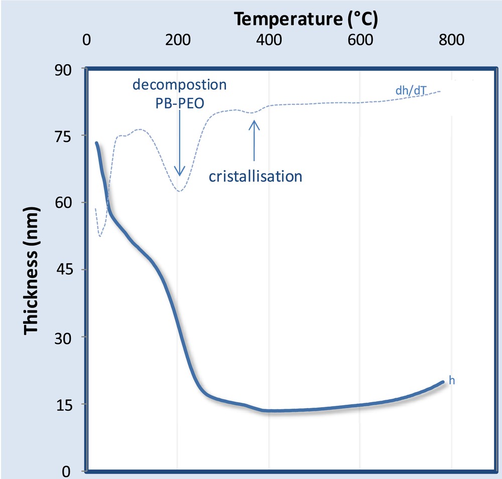
Evolution of thickness versus temperature of PB-PEO / ZrO2 layer through thermal ellipsometric analysis (TEA).
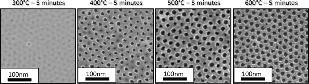
SEM top view of TiO2 nanoperforated layers after thermal treatment at 300 °C, 400 °C, 500 °C and 600 °C for 5 minutes.
2.7 Versatility of INPs towards perforation size and periodicity
As described in the previous sections, a wide range of patterns with variable perforation size and period can be obtained by modulating the chemical and processing parameters. Structural parameters and preparation conditions are detailed in Tables 1 and 2 for ZrO2 and TiO2. The PB-PEO templates were indicated with their commercial code as purchased by PolymerSource; the term e corresponding to the molar ratio water/ethanol was fixed to 0.11 for TiO2 and 0.17 for ZrO2. After deposition all the layers were treated at 500 °C for 5 min to ensure the complete decomposition of the block copolymer and the crystallization of the inorganic matrix.
2.8 Micro-patterning of INPs
The coupling between bottom-up and top-down processing is highly promising since complex hierarchical materials with additional functionalities can be potentially integrated into real devices [17,18]. Among the various top-down techniques, deep X-ray lithography (DXRL) is particularly suitable to process sol–gel materials since X-ray radiation acts as a cross-link promoter and leads to the local densification of the exposed structure while the unexposed material is removed by chemical etching [19]. In this example, the titania nanopatterned layers have been used as a resist for deep X-ray lithography in order to add a micrometric texturation to the system [20]. The whole process is illustrated in Fig. 11a. The titania-based INP was prepared as described in the previous sections. Directly after deposition (no thermal treatment), the hybrid film is exposed to X-rays through a DXRL mask. According to the literature [19], high energy X-ray radiation promotes the formation of free radicals H° and OH° from the residual water molecules present in the sol–gel film. Such radicals enhance the polycondensation kinetics of the inorganic part and thus the consolidation by cross-linking of the network. In addition, the ionization radiation causes bond-cleavage in the PB–PEO block-copolymer chains, initiating its decomposition and the consecutive formation of the porosity as confirmed by FTIR experiments. In the subsequent stage, the unexposed material and the organic residues of the exposed parts are removed by chemical etching. The final samples can be further thermally cured. An example of a micropatterned INP system on silicon is shown in the SEM images of Fig. 11. A micrometric array of hexagons (Fig. 11b) composed of nanoperforated TiO2 layers (Fig. 11c) is clearly observed. The same approach was used to fabricate hierarchical micro and nanoelectrode arrays that were obtained by processing the layer on a conductive Pt-coated silicon wafer [20].
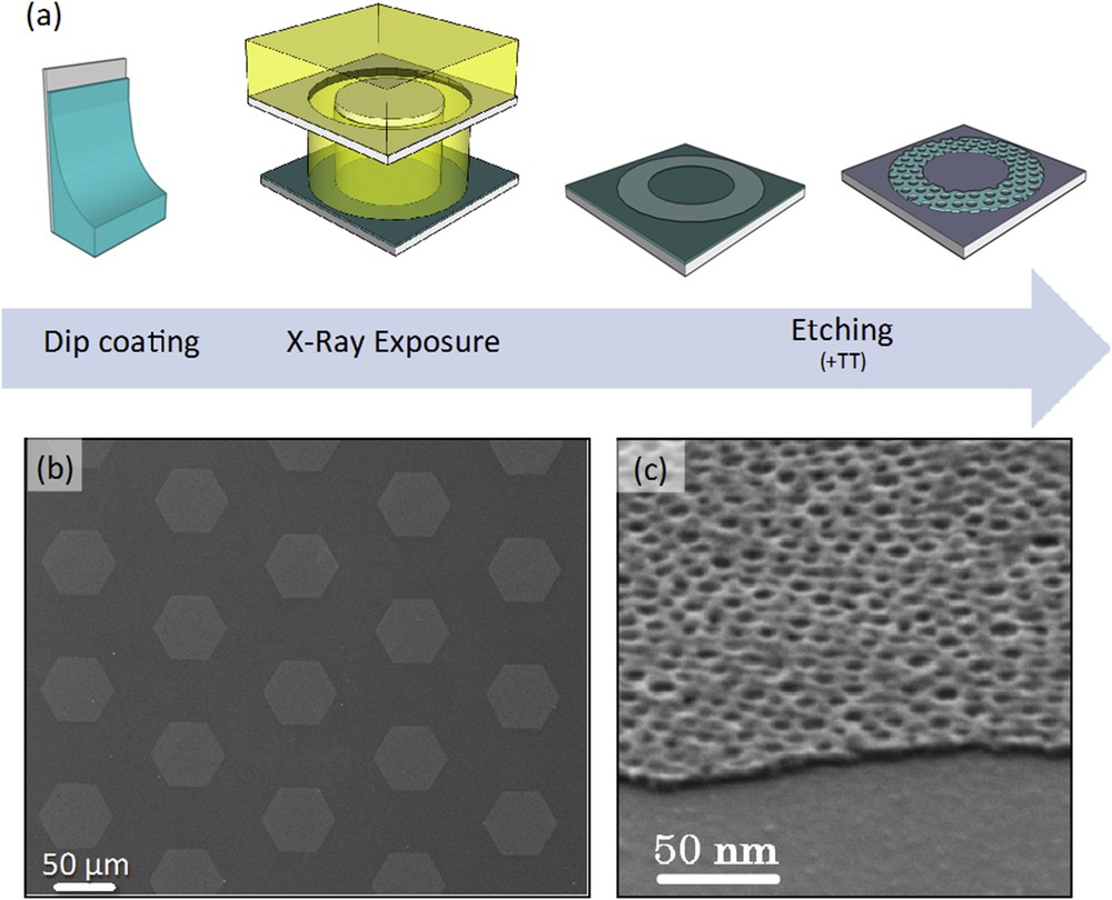
(a) Schematic flow diagram of the microfabrication process. SEM images of (b) the TiO2 micrometric hexagonal features and (c) details of the nanoperforated layer.
3 Applications in nanotechnology
3.1 Wetting
Constructing surfaces with controlled dispersion of surface energy at the nanoscale and understanding their interaction with liquid phases are interesting in many fields of application, including lab-on-chip, tribology, sensing, electronics, or biotechnologies. INPs are ideal systems to investigate such aspects related to wetting since they offer the possibility to create model surfaces exhibiting a homogeneous dispersion of two materials onto a single surface with a controlled topography that would account for the roughness. TiO2 INPs on oxidized silicon substrates [9] or on a thin gold layer surface [21] were used as heterogeneous nanostructured surfaces for fundamental wetting investigations. Due to the different chemical affinity of the substrates and of the INP materials, the discrete SiO2 or gold patches found at the bottom of the perforations, and the thin continuous TiO2 network surrounding them, could be selectively grafted with hydrophobic perfluorinated chemical functions using suitable silane or phosphonate coupling agents. When not grafted, SiO2 and TiO2 surfaces remained hydrophilic while gold is intrinsically hydrophobic. Static and water dynamic contact angles were then measured for different perforation dimensions and for the 4 possible combinations (hydrophobic/hydrophobic; hydrophilic/hydrophobic; hydrophobic/hydrophilic; hydrophilic/hydrophilic). The results were then compared to predictions made using the various available models (Cassie, Baxter, Wenzel) and the experimental reference contact angles measured on the plane systems. Three different types of wetting were observed depending on the contrast conformation, and the volume of the sessile drop applied on the patterned surface. For hydrophilic INP systems, full wetting of the surface was observed regardless of the contact angle of the perforation bottom surface. When small volumes of water were used, static and advancing contact angles between 100° and 130° were measured on hydrophobic INP systems, regardless of the contact angle of the perforation bottom surface (Fig. 12b). In both cases, the hydrophilic properties of the continuous network seem to govern the wetting behavior. For hydrophobic INPs, the contact angles match what is expected from the Cassie-Baxter model for which a nanobubble of vapor is trapped within each perforation (Fig. 12c). When the volume of water is high, the contact angles are lower and could be fairly well described by a combination of the Cassie and Wenzel equation. Large hysteresis between advancing and receding angles are observed for perforations larger than 20 nm due to the pinning effect allowed by the hydrophilic patches homogeneously dispersed onto the hydrophilic surface as schematized in Fig. 12(a).
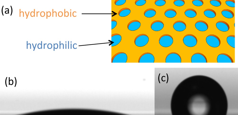
(a) Scheme of heterogeneous hydrophobic layer with hydrophilic patches. (b) Static water sessile drop on hydrophilic INPs and (c) hydrophobic INPs.
3.2 Photocatalytic surfaces
In all types of photovoltaic devices, the need for a sustainable optical antireflective coating on the top glass cover is a crucial issue to avoid the loss of photons due to reflection. The low refractive index required for these layers is usually achieved by a precise combination of silica and voids (porosity), with domains that must remain small enough to prevent scattering. It is however known that small pores tend to easily adsorb pollutants such as VOC, which induces increase of the coating refractive index and consequently reduction of its optical performances. These must then be continuously eliminated, which could be easily done by combining the TiO2 photocatalyst, already used in self-cleaning windows [22], with the porous layer [23]. However, such a combination would be required to dramatically increase the porosity of the film to compensate the high refractive index of TiO2, which would significantly decrease the mechanical stability of the layer. In order to overcome this issue, TiO2 INPs have been deposited on top of a sol-gel water repellent mesoporous silica film as shown in Fig. 13(a)[24]. The antireflective properties of the optical bilayer are only slightly affected by the presence of the INPs because of its extreme thinness (≈10 nm) and the presence of the perforations that reduce its refractive index down to 1.8. During the liquid deposition process, titania molecular intermediates do not infiltrate the pores of the underneath silica layer because of their stabilisation in the hydrophilic complexing shell of the block-copolymer micelles, that are much larger than the pores. This hard TiO2 INP top layer acts as a protecting barrier toward mechanical aggressions and brings high water wetting (antifogging) and photocatalytic (self-cleaning) properties. Indeed, the system shows an excellent capability to photo-decompose organic species that were adsorbed at the surface but also adsorbed in the anti-reflective (AR) layer pores as shown in the plot of Fig. 13 (b). It has been demonstrated latter that this decomposition takes place mainly through the diffusion of the pollutants towards the surface [25]. These bilayer multifunctional systems are easy to produce on a large scale at low cost and exhibit high mechanical and chemical durability. They are thus serious candidates to be used as antireflective, self-cleaning coatings for photovoltaic cells.
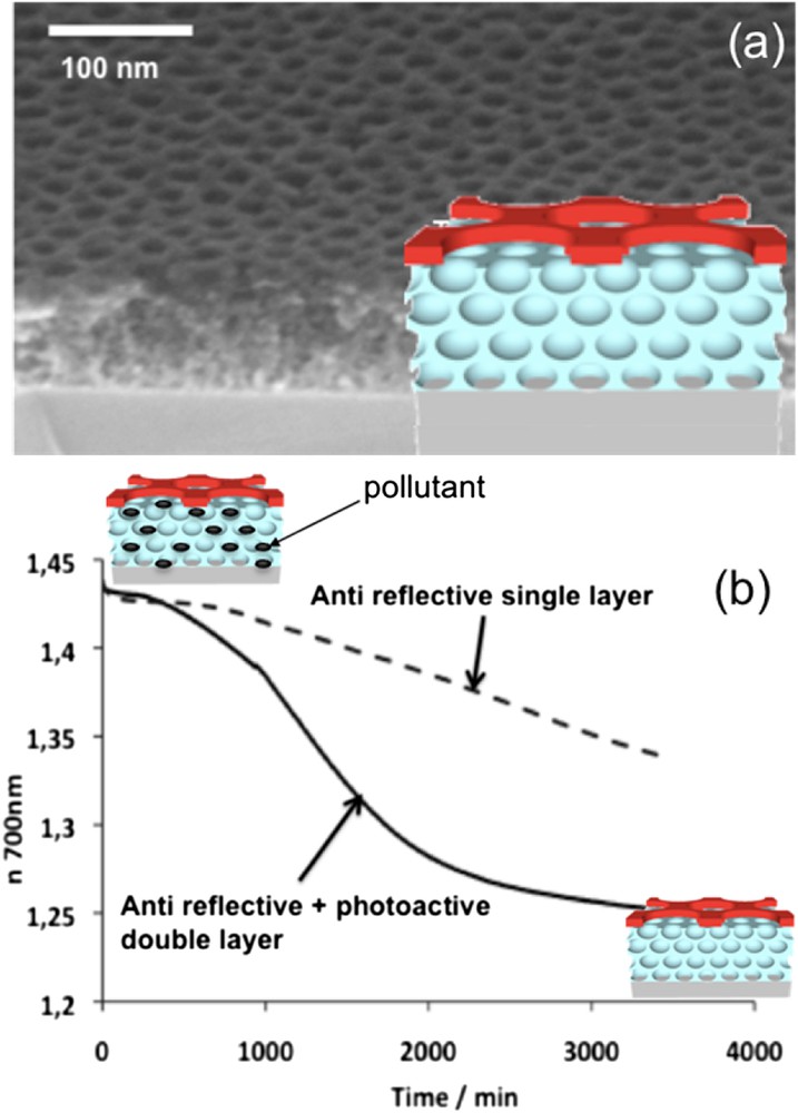
(a) SEM image and profile scheme of the anti-reflective, water repellent layer covered with self-cleaning TiO2 INPs. (b) Evolution of the refractive index versus time during the UV-decomposition of a pollutant for the anti-reflective layer with and without the INP photoactive layer.
3.3 Nanoelectrode arrays
Nanoelectrode arrays (NEAs) are defined as a collection of ordered electrodes. Their nanometer dimension allows for overlapping of linear and radial diffusion regimes, which is then exploited in analytical electrochemistry to enhance mass sensitivity through mass transport difference. They also operate in parallel, which amplifies the signal while the individual electrochemical properties of the nanoscale electrodes are retained [26]. Several more or less effective methods exist to construct NEAs, however none of them allows for simultaneous control over perforation size and dispersion, and membrane thickness. It was demonstrated that self-assembled block copolymer layers act as an efficient nanoperforated NEA surface [27], however they suffer from poor chemical and mechanical stability, which in fine make their use very restricted. In the present system, the nanoperforated polymer was replaced by TiO2 INPs [28] since the high thermal, chemical and mechanical stabilities of the TiO2 protective membrane is advantageous compared to the polymer. The latter thin layer was deposited and treated onto gold conductive substrates, such that the highly ordered nanoperforations mediate the transport of electroactive species to the underlying electrode surface. These surfaces constitute the first examples of NEA devices where a ceramic matrix is used to delimitate conducting discoid nanopatches having very small dimension. Perforations of 17 nm in physical diameter, separated by 26 nm, and allowing for 74% of the surface to remain electroactive, have been evidenced. The cyclic voltammetry and galvanostatic investigations revealed that these NEAs exhibit characteristic overlapped regimes of diffusion associated with enhanced red/ox probe sensitivity (see Fig. 14) [29,30]. These INP NEA surfaces were then modified by growing polymers (poly(phenylene)oxide) by anodic electro-polymerisation at the bottom of the discrete gold nanodisk electrodes or by attaching a functional group ((CF3–(CF2)2–(CH2)5O)2POO–) locally to the continuous ceramic network [28]. Because the polymer can act as a semi-permeable membrane, it can limit the transport of specific molecules, solvent, or reactants to the gold surface. In addition, the bi-dimensional network interface, which can thus be tuned in terms of surface chemical composition by specific functionalization, would influence the diffusion layer extent, the chemical interaction, and the adsorption capacity near the nanoelectrode. Such complex hybrid electrodes would combine the advantages of NEA sensitivity with an adjustable surface energy and a semipermeable membrane. Moreover, if the polymer is thermoresponsive, the response of the NEA can be tuned by changing the temperature. Such an ability to modify the surface of these NEAs opens a promising route to elaborate complex electrochemical devices suitable for analytical chemistry like biosensors, sensors, etc. As already mentioned, because the latter system can be patterned using deep X-ray lithography, complex NEA surfaces and devices can also be constructed [20]. Such TiO2 INP NEAs have also been used to selectively grow metals and alloy nanoparticles within the perforations [31]. More recently, tin-rich ITO nanoperforated electrodes, bearing a single Au nanoparticle per perforation, were prepared using an evaporation-induced hydrophobic nanoreactor templating (EIHNT) approach. These nanoperforated composite electrodes have shown enhanced electrocatalytic activities in the CO oxidation reaction compared to non-perforated electrodes [32].
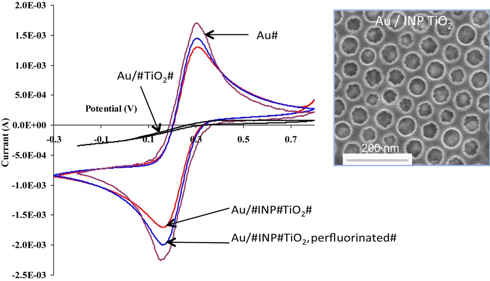
Cyclic voltammograms of 1 mM Fe(CN)6 in KCl collected on Au electrodes (bare, or covered 20 nm dense TiO2 , INP TiO2 and INP TiO2 perfluorinated); inset: SEM image of Au/INP TiO2 typical system bearing large perforations.
3.4 HyLEDs
Hybrid organic-inorganic light emitting diodes (HyLEDs) are novel devices with inverted organic LED structures that have proved to have efficiencies comparable to polymer LEDs. Competitive light emitting hybrid devices must deal with the optimization of light emission and efficiency through the reduction of the exciton quenching and of the decrease of the current density leakage at the organic/inorganic interface. The typical structure of a hybrid LED is made of an electron transport layer (ETL), an n-type transition metal oxide (e.g., ZnO, TiO2, ZrO2), deposited onto the indium-doped tin oxide (ITO) cathode, followed by the successive deposition of the light emitting polymer active layer (LEP), the hole transport layer (HTL), and finally the metallic anode. Electrons are injected through the ITO into the conduction band (CB) of the ETL, and into the LUMO of the LEP. However, the mismatch between these two energy levels results in a barrier for electron injection. Additionally, the mismatch between the ETL valence band and the HOMO of the LEP results in the accumulation of positive charges at the ETL/LEP interface. It is assumed that this built-up field enhances electron injection into the LEP despite the energetic barrier, and allows the subsequent electron–hole recombination. The decay of this excited state is accompanied by the emission of radiation whose frequency is in the visible range. Issues for the optimization of the HyLed efficiencies are the interfacial contact and the energy level alignment between the active ETL and LEP layers. Therefore, the morphology at the ETL/LEP interface determines the device efficiency. The ZrO2 INP (thickness < 10 nm and perforation diameter around 60 nm with periodical distance of 90 nm) layers have been intercalated between both plane ZrO2 ETL and F8BT ((poly-9,9′-dioctyl fluorene-co-benzothiadiazole, maximum emission at 540 nm)) LEP layers to address both issues at once [33]. This system showed the best modulation of the current density leading to record efficiencies of 13.8 cd/A and 4.6 lm/W, one order of magnitude higher than what was obtained for the INP-free devices. This improvement was attributed to the presence of the nano-perforated layer at the ETL/LEP interface that increases the surface area, which thus extends area for injection, and that enhances hole-blocking through increase of the ETL thickness. Because the F8BT polymer shows an excellent charge transport in the parallel and perpendicular directions to the substrate, the nano-perforations provide an excellent pathway for charge injection and recombination, reducing the charge density reaching the electrodes. It was also assumed that a more intimate contact between the surface of the nanoperforated ZrO2 and the polymer has been achieved, compared to the dense films. This better contact favors charge recombination that results in the enhanced luminance and the reduction of the charge density.
4 Applications in nanofabrication
4.1 Nanomasks for pattern transfer
The development of bottom-up methods to prepare large nano-patterned surfaces is stimulated by requirements in large area electronics, photovoltaics, displays, or integrated smart systems. While top–down lithographic approaches yield extremely well resolved periodical feature arrays with dimensions as small as 20 nm, they remain slow, costly and have low throughput and thus not directly appropriate for industrial production on large surfaces. Bottom-up approaches are capable of self-assembling organic [34] and inorganic materials [35] of much smaller dimensions using liquid deposition, but they suffer from poor long-range order and the presence of localized points and extended defects. They can thus be used as a cheap alternative or an intermediate step in conventional nanofabrication protocols. Self-assembled nanosphere arrays [36] or block copolymer nanostencils [37] have been used in combination with reactive ion etching (RIE) for transferring 20–50 nm features with hexagonal or square organisation on Si wafers, but their implementation at the industrial scale is not straightforward. Another alternative is to use the robust and simple to prepare sol–gel derived INPs as self-assembled reactive nanomasks (RNMs) [38] for lithographic transfer through dry etching as shown in Fig. 15. The distinctive feature of the latter RNMs is that they can react with the etching plasma to yield a highly stable, and thus highly selective, stencil. The present INP RNM is composed of CaxTi(1−x)O(2−x) so that Ca2+ can react with the fluoride species of the plasma to yield CaF2, while Ti species are etched away. The formal calcium titanate INP is thus replaced by calcium fluoride, a solid compound that is extremely stable under the present etching conditions, without changing the initial lateral morphology. Using this approach, and depending on the perforation size and the Ca2+ concentration of the initial mask, transfer of ordered arrays of Si vertical pillars or wells, having diameters down to 20 nm and height, or depth, of 200 nm could be achieved. This novel concept combines simple self-assembly with RIE to achieve features up to 1:25 selectivity and aspect ratio up to 8. These novel RMNs are homogenous, robust, and they can be applied on a surface size limited only by the capacity of the RIE device. In addition, the complete process (mask fabrication + dry etching) can be performed within only 15 min. This versatile approach is thus likely to be a promising candidate for the industrial large surface production of electronic and optical components.
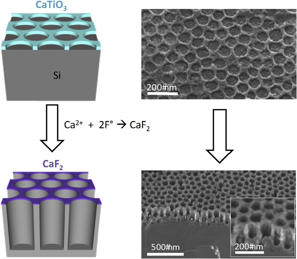
Scheme of the pattern transfer (left) and corresponding SEM images (right) of the INP initial nanomask and of the etched surface.
4.2 Nanomask for LBL growth of photomagnetic nanodots
Molecular materials that exhibit bistability in their physical properties as a function of external stimuli, such as light or electric field, offer appealing perspectives for the realization of molecular-scale electronic devices [39]. In most cases, these functional materials need to be integrated as nanodomains within planar devices in specific locations or/and under controlled dispersion. TiO2 INPs have been used here as self-assembled heterogeneous substrates to selectively guide the growth of photomagnetic bistable CoFe Prussian blue analogues (PBAs) nano-objects [40] within the nanoperforations [41,42]. The selective and controlled growth was achieved through INP functionalisation followed by molecular layer-by-layer (LBL) deposition. The INPs were first prepared onto Au substrates with thickness around 10 nm and a perforation diameter of 60 nm. The titanium oxide network was then simply passivated with phenyl hydrophobic groups, while the Au nanopatches were activated with carboxylic acid groups. Both selective functionalisations were done using phosphonate and mercaptopropyl coupling agents, respectively. The carboxylic acid functions play the role of active nucleating centers in initiating the PBA growth by LBL from the perforation bottoms only. The grafted system was then immersed in successive aqueous solutions containing each of the PBA precursors (hexaaquacobalt (II), hexacyanoferrate (III), and Rb (I)). Washing in water is performed between each immersion. The thickness of the PBA multilayer can be adjusted by tuning the number of cycles, and the chemical composition of the PBA can be varied at will by the choice of the precursors. It is important to precise that the formation of the nanodomains at the position of the perforations is achieved only if the pre-functionalisation of both TiO2 and Au is done (see Fig. 16a). The magnetization of the PBA/INP film after irradiation at 10 K with λ = 642 nm and 50 mW cm−2 excitation power is higher than the magnetization of the film before. The initially diamagnetic Co III (LS)/Fe II (LS) PBA is trapped in the paramagnetic Co II (HS)/Fe III (LS) metastable state after irradiation at low temperature and the thermal relaxation occurs at 55 K, suggesting that these small domains can be optically addressed. As expected for nanosized particles, the collective magnetic bistability associated with the long-range magnetic order is lost whereas the molecular electronic bistability associated with the electron transfer persists. The periodically organized nanoperforations filled with photomagnetic PBA can be seen as data bits, which could, a priori, be optically addressed separately.
TiO2 INPs bearing (a) PBA and (b) FePt nanoparticles.
4.3 Nanomask for salt-assisted magnetic nanodot deposition
As for the PBA, nanometer-scale assemblies of permanent magnets on surfaces would constitute magnetic data storage or spintronic devices. One of the most promising materials for magnetic applications is FePt alloy in the face-centred tetragonal (fct) phase since it is known to exhibit large magneto-crystalline anisotropy and high coercivity at room temperature. The major challenges that have to be faced for achieving such complex systems are the preparation of hard magnetic FePt nanoparticles with permanent residual magnetization and their positioning on the surface by a controlled and versatile process. In this context, magnetic nanocomposite surfaces composed of hard magnetic FePt nanoparticles into TiO2 INPs, were prepared by controlled chemical solution deposition of hexaaquairon(II) hexachloroplatinate, ([Fe(H2O)6][PtCl6]) salt into the INP perforations, followed by its direct transformation into the FePt (fct) phase by thermal annealing at 400 °C in a reductive atmosphere (see Fig. 16b) [43]. This strategy exploits the dip-coating process that is highly suitable to homogeneously impregnate porosity as a result of the progressive evaporation that tends to drag solutes within the porous network upon solvent departure [44]. In addition by carefully modulating the deposition conditions, the dip-coating process enables exact control of the amount of material that can be applied onto the substrate [13]. The magnetic properties of these systems have been investigated by SQUID. The H–M curve shows typical hysteresis loops. At 300°K, the TiO2/FePt system reveals a coercivity of 899 eO that indicates the presence of hard magnetic nanoparticles, confirming the effectiveness of the transformation from salt to the fct phase locally in the nanoperforations.
4.4 Nanomasks for magnetically percolated perpendicular media
The demand for higher storage capacities is one of the driving forces in the development of innovative magnetic materials and several novel concepts for magnetic recording are being explored to achieve above 1 Tbit/ in2 [45] areal densities. One of the proposed approaches is based on percolated perpendicular media (PPM), which consists of an exchange coupled magnetic film with a dense distribution of defects which serve as pinning sites for magnetic domain walls [46]. Several experimental realizations of PPM have already been reported through codeposition of the magnetic material and nonmagnetic oxides [47], magnetic films on anodized alumina templates [48], and the deposition of hard magnetic materials on arrays of nonmagnetic nanoparticles [49], to name a few. An alternative route based on the deposition of hard magnetic CoPt films on nanoperforated ZrO2 has also been proposed [50,51]. Two ZrO2 nanoperforated surfaces with an average perforation diameter of 67 nm and a period of about 110 nm for the first one, and with an average perforation diameter of 17 nm and an average period of 34 nm for the second one were used. In these systems, as displayed in Fig. 17 (c), the nanoperforations act as pinning sites for the magnetic domain walls, while the exchange coupling between the magnetic material inside the nanoperforations and the continuous film outside can be used for tuning the pinning strength. 4.8-nm-thick Pt seed layer was deposited onto the substrates, followed by 8 repetitions of 0.28 nm Co/0.76 nm Pt bilayer and a 2 nm Pt cover layer using a dc-magnetron sputter technique as shown in Fig. 17(b). The recording performance of these two samples was investigated by scanning magnetoresistive microscopy using conventional hard disk read/write heads having a magnetic write width and magnetic read width of about 110 nm and about 70 nm, respectively [52]. The size of the magnetic domains that can be written by a recording head is limited by the spacing between pinning sites induced by the nanoperforated INP template surface. Due to the period of 110 nm on the sample with the larger perforations, the minimum bit pitch is expected to be on the order of 200 nm. In this case, domains written with a smaller bit pitch merge together as observed experimentally. Fig. 17(d) shows the read back image for various bit periodicities written on the sample with smaller perforations. On the sample with a period of 34 nm, the individual domains can be clearly separated even at a bit pitch as low as 100 nm, close in dimension to that of the head read/write characteristics. Based on the signature of the pinning controlled domain wall movement for percolated media, a zero field energy barrier of 93 kBT is determined by fluctuation field measurements and is elucidated by micromagnetic calculations using the nudged elastic band method. This value is sufficiently large to qualify the material as promising percolated media [53]. It is proposed that further optimization of the magnetic layer stack, including the use of a soft magnetic underlayer, of a hard scratch resistant overcoat and lubricant, might still increase the recording performance of this type of PPM.
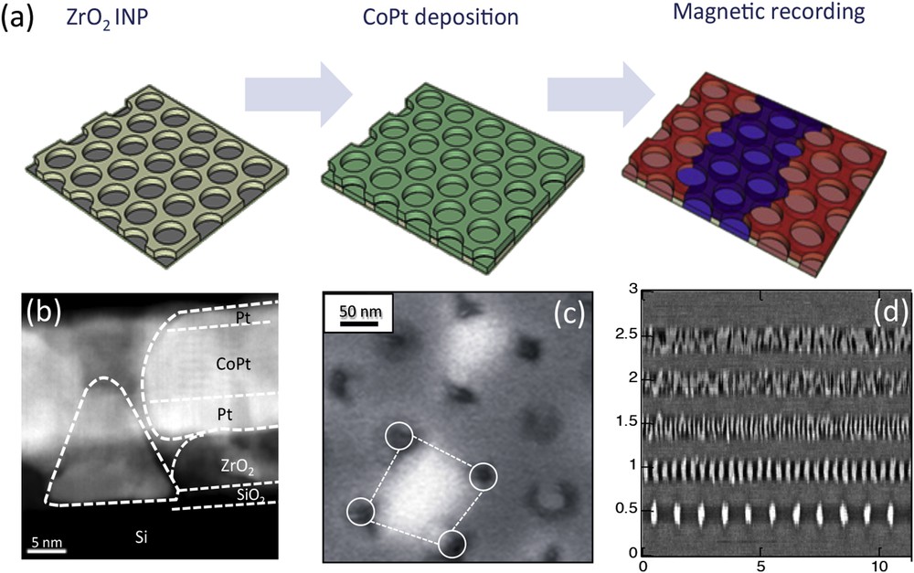
(a) Schematic illustration of the deposition process and recording of ZrO2 /CoPt magnetic nanocomposites. (b) HR-TEM cross section of the ZrO2 /CoPt system. (c) MFM images of the system highlighting one single magnetic domain stabilized by “pinning”. (d) MFM image of the ZrO2 /CoPt nanocomposite with 17 nm large perforations after magnetic recording test.
4.5 Nanomasks for controlled solid dewetting of semiconductor nanodots
Self-organized germanium (group IV semiconducting materials) nanoparticles, for which the quantum confinement effect provides an additional engineering dimension to tune the emission wavelength, are of particular interest for applications in optoelectronics, or nanocrystalline memory devices [54]. The electron–hole recombination induced photoluminescence (PL) in Ge nano-crystal dots is dependent on the quantum confinement states and occurs in the near IR infrared and in the visible region [55]. It is known that dot size affects the bandgap energy Eg, and that the PL spectrum can be predicted using theoretical models [55]. Here, germanium dots have been formed by a dewetting process that occurred during an in situ thermal annealing at 450 °C of an amorphous Ge layer deposited by molecular beam epitaxy on a thin nanoperforated TiO2 layer prepared on SiO2/Si(001) [56–58]. Three different TiO2 nanoperforated thin layers, having perforation sizes between 10 and 50 nm, were used to modulate the dimensions of the nanodots during solid dewetting. The dot size measured by AFM revealed that particles were in the range of 10–35 nm depending on the sample. Larger particles were found for larger perforations and thus larger periodic distance of the TiO2 pattern substrates, suggesting that the variation of surface free energy, related to the presence of the heterogeneous nanoperforated TiO2 layer on the Si wafer, is efficient to govern the nucleation growth and dispersion of crystalline Ge nanoparticles from thermal annealing of an initial amorphous continuous layer. The PL measurements performed on such self-assembled systems are shown in Fig. 18 and reveal an emission as a wide near-infrared band between 0.7 and 1 eV. An analysis of the PL response with respect to theoretical predictions of the bandgap versus dot size allowed an assessment of the size dependence of the PL quantum efficiency in Ge dots. Good qualitative agreement was obtained between the PL-derived dot size distributions and those from AFM. Further work showed a nonlinear increase in the PL efficiency with decreasing dot diameter, suggesting that dot PL spectra used in conjunction with the theory provided a promising method to evaluate Ge dot size distributions [59]. The latter approach confirms that oxide nanoperforated surfaces with controlled motif dimension and periodicity can be used to control the size of metallic Ge nanodots formed by solid dewetting. This method could then be further applied to other interesting dot/substrate systems that require controlled distribution of nanoparticles onto a specific surface.
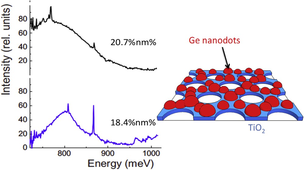
Photoluminescence spectra recorded at 5 K with a 20 mW excitation laser (458 nm) for two different populations of Ge nanodots on TiO2 INPs having two different average diameters (20.7 and 18.4 nm). Inset: scheme of the Ge nanodots formed by dewetting on TiO2 INPs.
5 Conclusions
The latter examples showed that INPs obtained by the self-assembly of a single layer of block copolymer micelles in the presence of suitable inorganic sol-gel precursors during controlled dip-coating have potential interest in many fields of nanotechnology and nanofabrication. This is related to the versatility in adjusting the INP chemical composition together with the perforation dimensions and separation distance, to the chemical–mechanical and thermal stability of the material, and to the ease of preparing very large surfaces at low cost. Despite the already very promising results, it is with no doubt that such INP systems will become more and more appealing and that other types of composition and combination will soon see the light of day.
Acknowledgements
We thank the funding agencies together with the students, the post-docs and the collaborators that were involved in the development of these inorganic nanopatterns in the past years.