1 Scope of nanoscience in environmental chemistry
In this new millennium, we are faced with the challenge of cleaning our natural water and air resources. While we enjoy the comforts and benefits that chemistry has provided us, from composites to computer chips, from drugs to dyes, we are faced with the task of treating wastes generated during manufacturing processes and the proper disposal of various products and byproducts. Nanotechnology can provide us ways to purify the air and water resources by utilizing semiconductor nanoparticles as catalysts and/or sensing systems. Furthermore the utilization of light and ultrasound to activate such nanoparticles opens up new ways to design green oxidation technologies for environmental remediation.
The size and shape dependent optical and electronic properties of nanoparticles make an interesting case for environmental chemists to exploit their role in environmental remediation processes [1–5]. Of particular interest is their application in advanced oxidation processes [6]. TiO2 nanoparticles have been extensively studied for oxidative and reductive transformation of organic and inorganic species present as contaminants in air and water. Technological advances in this area have already led to product development for a variety of day-to-day operations. Commercialization of products such as self-cleaning glasses, disinfectant tiles and filters for air purification demonstrates the early successes of nanosystems for environmental applications [7].
Maximizing the efficiency of photoinduced charge separation in semiconductor systems remains to be a major challenge to the scientific community. Obtaining insight into charge transfer processes is important to improve the photoconversion efficiencies in semiconductor-based nanoassemblies. Earlier reviews [8–10] have focused on the principles and mechanism of photocatalytic reactions in advanced oxidation processes. We present here some of the recent developments related to semiconductor nanoparticles in advanced oxidation processes.
2 Semiconductor nanoparticles as phototocatalysts
The participation of a semiconductor nanoparticle in a photocatalytic process can be either direct or indirect as illustrated in Fig. 1a and b respectively.

Photoinduced charge transfer processes in semiconductor nanoclusters. (a) Under bandgap excitation and (b) sensitized charge injection by exciting adsorbed dye molecules. CB and VB refer to conduction and valence bands of the semiconductor.
Charge separation in semiconductor particles occurs when they are subjected to bandgap excitation. The photogenerated electrons and holes are capable of oxidizing or reducing the adsorbed substrates (Fig. 1a). Alternatively the semiconductor nanoclusters also promote a photocatalytic reaction by acting as mediators for the charge transfer between two adsorbed molecules (Fig. 1b). This process, which is commonly referred to as photosensitization, is extensively used in photoelectrochemistry and imaging science. In the first case, the bandgap excitation of a semiconductor particle is followed by the charge transfer at the semiconductor/electrolyte interface. However, in the second case, the semiconductor nanoparticle quenches the excited state by accepting an electron and then transfers the charge to another substrate or generates photocurrent. In the present context, the contaminant dye itself acts as a sensitizer and undergoes oxidative degradation. Such an approach (Fig. 1b) was found to be useful in discoloration of the textile dye on TiO2 nanoparticles [11, 12]. The energy of the conduction and valence bands of the semiconductor and redox potential of the adsorbed molecule control the reaction course of the photochemical process.
The TiO2 photocatalyst has been the popular choice of much of the published photocatalysis work. Its large bandgap energy (3.2 eV) necessitates UV excitation to induce charge separation within the particle. In a pioneering article of 1955, Markham pointed out the photocatalytic properties of zinc oxide, titanium oxide and antimony trioxide under UV irradiation [13]. In aqueous solutions, the holes are scavenged by surface hydroxide groups to generate •OH radicals, which then induce the oxidation of organics [14–18]. The •OH radical mediated oxidation has been successfully employed in the mineralization of many chemical contaminants. Interestingly, electron scavenging becomes the rate-limiting factor in such oxidation processes [19–25]. Alternative methods have also been suggested to promote the charge separation by applying an electrochemical bias to a TiO2 particulate film electrode [23]. On the other hand both reductive and oxidative steps can be beneficially used to degrade aromatic compounds such as trinitrophenol [26].
Several research groups have attempted to extend the photoresponse into the visible by doping the TiO2 with transition metal ions. In many instances, such doping procedure directly influences the intrinsic properties of the semiconductor and extends its photoresponse into the visible [27–29]. Nitrogen doped into substitutional sites of TiO2 has shown bandgap narrowing as well as photocatalytic activity in the visible [30]. Films and powders of TiO2–xNx have shown an improvement over TiO2 under visible light (up to 500 nm) irradiation. Arakawa and coworkers have synthesized a photocatalyst that produces stoichiometric amounts of oxygen and hydrogen under visible light irradiation [31]. The bandgap change in these Ni-doped indium tantalum oxide compounds was attributed to internal transitions in a partly filled Ni d shell and is characterized by the absorption band at 420–520 nm.
Another approach to utilize the visible light for inducing a charge transfer process in a large bandgap semiconductor system is to modify the surface with a sensitizing dye such as Ru(II) polypyridyl complex [32]. The electron injected into the semiconductor is transferred for the reductive transformation of a pollutant such as CCl4 [33]. However, if one is interested in making use of the dye molecule as an active sensitizer, one needs to address the stability issues related to dye regeneration. While charge injected from excited Ru(II) polypyridyl complex into TiO2 can be efficiently utilized for the reduction of an organic molecule such as carbon tetra chloride [33], it is necessary to regenerate the oxidized sensitizer with another sacrificial electron donor. Failure to regenerate the sensitizer will eventually cause the degradation of the sensitizer [34].
3 Semiconductor-metal nanocomposites for improving the efficiency of photocatalytic processes
By designing semiconductor–metal composite nanoparticles, it is possible to improve the catalytic properties of photocatalysts (Fig. 2). Contact of metal with the semiconductor indirectly influences the energetics and interfacial charge transfer processes in a favorable way. The deposition of a noble metal on semiconductor nanoparticles is an essential factor for maximizing the efficiency of photocatalytic reactions [35]. It is commonly assumed that the noble metal (e.g., Pt) acts as a sink for photoinduced charge carriers and promotes interfacial charge transfer processes.

Charge-transfer and Fermi-level equilibration in a metal–semiconductor nanocomposite. E′F and EF refer to Fermi levels before and after equilibration.
Metal islands or nanoparticles deposited on a semiconductor surface undergo Fermi level equilibration following the charging with photogenerated electrons. The effect of Fermi level equilibration is predominantly seen when the metal deposits consists of small islands or small particles. Unlike bulk metals, the nanoparticles do not often exhibit ohmic contact with the semiconductor surface which retain the charge before transferring them to the redox species. During extended UV photolysis, electron capture by metal islands of Ag, Au and Cu becomes inhibited as their Fermi-level shifts close to the conduction band of the semiconductor. Pt on the other hand acts as an electron sink and fails to achieve Fermi-level equilibration. Based on the photoelectrochemical study a Fermi-level shift of about ~150 mV was observed for the TiO2/Au composite film [36, 37]. The metal nanoparticles deposited on TiO2 films thus proved beneficial for improving the photoelectrochemical and photocatalytic performance (Fig. 3).

Energy-level diagram illustrating the role of A. Pt and B. Au in dictating Fermi level equilibration of ZnO–Metal composite system (from [38]).
Photoelectrochemical studies [36, 39] carried out by depositing gold nanoparticles on nanostructured TiO2 films exhibit enhanced photocurrent generation. Improved interfacial charge transfer at the semiconductor/electrolyte interface resulted in nearly three-time enhancement of photocurrent generation and a shift in the apparent flat band potential. Although the TiO2@Au interface may offer many complex scenarios, the photoelectrochemical and photocatalytic measurements support the argument that the metal nanoparticle deposition facilitates charge (electron) stabilization in nanostructured TiO2 films and promote interfacial hole-transfer processes.
3.1 Sensing the chemical environment with semiconductor nanostructures
A variety of sensors for environmental applications have been developed in recent years, including SnO2–based semiconductor systems that have been used as conductometric gas sensors [40, 41] and a TiO2 electrode for determining the chemical oxygen demand (COD) of water [42]. The system that has drawn attention in recent years vis-à-vis its potential to be used as chemical sensors is semiconductor nanostructures. Prompted by the discovery of photoluminescence from porous Si and subsequent observation that many organic and inorganic molecules quench this emission, has led to their exploitation as chemical sensors [43, 44]. The photoluminescence in porous Si arises from charge carrier recombination in the quantum confined nanosized environments [45, 46]. Both energy– and electron-transfer mechanisms have been proposed to explain the quenching by organic molecules. Sailor et al have attributed the quenching of the PL by aromatic molecules such as anthracene, pyrene, benzanthracene etc. to energy transfer to the triplet state of the organic substrate [47]. El-Shall and coworkers [48] have shown that the emission from silicon nanocrystals is quenched by aromatic nitrocompounds via electron transfer from the conduction band of the silicon nanocrystal to the vacant orbitals of the quenchers.
The feasibility of using porous silicon nanocrystals as sensors has been demonstrated for detecting nerve gas agents [49] and nitroorganics [48, 50]. Using detection based on electrical conductivity [51], photoluminescence [49, 50], or interferometry [49], researchers have achieved sensitivity in the range of ppb–ppm levels.
3.2 Simultaneous detection and degradation of low-level organic contaminants
A desirable feature for the detoxification of air and water is to develop methodologies that can simultaneously sense and destroy toxic chemicals. Such a catalyst system is especially useful when it triggers the photocatalytic operation on demand, i.e., photocatalysis becomes operational only when the system senses the presence of an aromatic compound in the immediate surrounding. Semiconductor nanoclusters such as ZnO and CdSe have an added advantage that they emit quite strongly in the visible region. Size-dependent emission properties of these semiconductor systems have been explored in earlier photochemical studies [52–56]. The size-dependence properties of these nanoparticles and the ability to tailor the sizes of the nanoassemblies find ready application in chemical sensors. The thermal conductivity of metal oxide semiconductors is often used to sense organic vapors and gases [57]. The visible emission of nanosized ZnO, which usually arises from anionic vacancies, is very sensitive to hole scavengers [56].
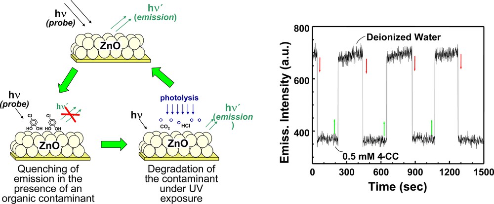
ZnO is a promising candidate for such a specialized environmental application (Fig. 4). The visible emission of ZnO, which usually arises from anionic vacancies, is very sensitive to hole scavengers. The emission is quantitatively quenched by hole scavengers such as iodide ions or phenols [59]. The feasibility of employing nanostructured ZnO films for simultaneous sensing and degradation of organic contaminants has been demonstrated recently in our laboratory [58]. The ZnO emission is very sensitive to the presence of aromatic compounds such as chlorinated phenols in water. The observed emission quenching is quantitative as the extent of quenching by the organics is determined by the adsorption equilibrium. A detection sensitivity of the order of 1 ppm can be achieved in these systems. A major feature of the ZnO semiconductor system is its ability to degrade the organic contaminant under high-intensity UV illumination.

Principle of simultaneous detection and degradation approach in photocatalysis. The emission response of ZnO film to the presence of 4–chlorocatechol is shown on the right. (From [58]).
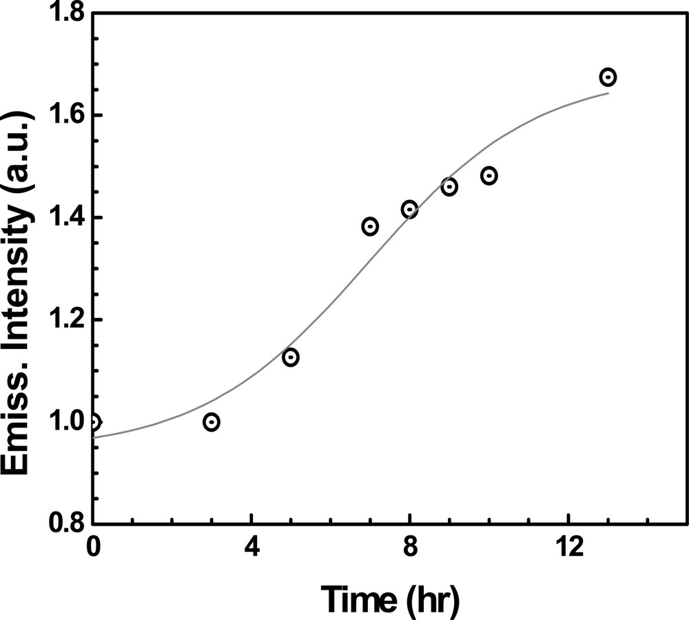
Experiments illustrating the emission increase during photocatalytic degradation (Fig. 5) show that the emission recovery parallels the degradation of aromatic intermediates from the aqueous solution. Thus, emission from ZnO films can be used to monitor the course of a photocatalytic reaction. Though not selective, ZnO emission quenching serves as a probe to sense the presence of aromatic intermediates in water. ZnO film-based nanosensors should be useful in applications such as monitoring the quality of drinking water, or assessing the contamination in underground water. Design engineering of fiber optic probes can miniaturize the sensor for environmental applications.

Emission recovery during the degradation of 4–chlorophenol at an UV-irradiated ZnO film (from reference [58]).
3.3 Combining photocatalysis with other advanced oxidation processes (AOP)
Combining photocatalysis with another AOP such as sonolysis could be an effective approach to improve the mass transfer of reactants and products to and from the catalytic surface in photocatalytic reactions [60–64]. While hydroxyl radicals play a role in TiO2 photocatalysis, direct hole induced oxidation on the catalyst surface opens up an alternative route in the degradation mechanism [65]. Many organic compounds are readily broken down, but others are not readily transformed by this heterogeneous oxidation system. The TiO2 photocatalysis process is most useful in its ability to rapidly degrade polar compounds. When highly polar compounds are formed during the oxidation of organic contaminants, complete breakdown to CO2 and H2O (mineralization) is quickly realized.
Since the strengths of sonolysis and photocatalysis are complimentary, a system that employs them together seems a worthwhile endeavor. We tested a combination of sonolysis and photocatalysis in both a simultaneous and a sequential manner using the dye naphthol blue black as the model pollutant [66]. In addition to increasing the rate of degradation and mineralization of environmental contaminants, the combinative approaches are implemented to solve the problem of toxic intermediates that often accumulate as chemical intermediates during the degradation process.
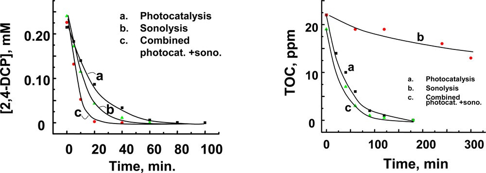
The merits of combining sonolysis and photocatalysis were evaluated by investigating the degradation of an azo dye, naphthol blue black (NBB) [66] and an herbicide, 2,4-dichlorophenoxyacetic acid [67]. Experiments were carried out by employing a high-frequency ultrasonic generator and UV photolysis simultaneously. Fig. 6 shows the degradation of 2,4-D and the decrease in TOC observed during the sonolysis, photocatalysis and combined sonolysis and photocatalysis experiments. An additive effect on the degradation rate of the parent compound was observed when the sonolysis and photocatalysis experiments were carried out together. Whereas sonolysis was effective in the initial degradation of 2,4-D, photocatalysis was more efficient in decreasing the TOC. Moreover, the combined approach also minimizes the production of chemical intermediates such as chlorinated phenols [67]. The combination approach overcomes the deficiencies of the individual techniques and makes the overall remediation process more effective. The added benefit of sonication on photocatalysis also stems from several other sources. For example, during combined sonolysis and photocatalysis experiment we expect the photocatalyst to be well dispersed and its surface constantly refreshed. This mass transport of reactants and products to and from the catalyst surface improves as the slurry is constantly agitated.

A. Degradation of 2,4–D. B. Decrease in total organic carbon (TOC) during (a) photocatalytic, (b) sonolytic and (c) combined photocatalytic and sonolytic degradation of 2,4–D in aqueous solution (from [67]).
One of the major concerns in any Advanced Oxidation Process is the formation of undesirable reaction intermediates. It is not unusual to observe several intermediates with toxicity greater than the parent compound itself. Rapid mineralization of an organic contaminant should be the goal. Minimizing the survival time of toxic intermediates is prerequisite to obtain fast mineralization. A combinative AOP approach could serve as a solution to tackle such an issue. While analyzing the merits and deficiencies of sonolysis and photocatalysis, several complimentary aspects of these two processes were noted. Table 1 summarizes the salient features of the two advanced oxidation processes and highlights the benefits of the combined approach in the mineralization of 2,4–dichlorophenoxyacetic acid. Quick degradation and mineralization of the chlorinated organic compounds is induced by carrying out sonolysis and photocatalysis simultaneously. More importantly, no build-up of toxic intermediates such as chlorinated phenols is detected in the combination experiment.
Comparison of salient features of different advanced oxidation processes†
| Feature | Sonolysis | Photocatalysis | Combined Sonolysis and Photocatalysis |
| Degradation of non-polar compounds | good | variable | very good |
| Degradation of polar compounds | poor | good | very good |
| Mineralization | poor | good | very good |
| Avoidance of toxic intermediate | good | poor | very good |
| Need for a catalyst | no | yes | yes, in smaller quantity |
4 Scope of future research
In recent months concerns have been raised regarding the adverse impact of nanotechnology on environment [68]. It should be noted that most of the nanotechnological advances are based on known chemicals and materials that are already employed in various applications. The novel aspect of nanotechnology has been to organize the molecules into clusters or assemblies so that the properties of the produced nanomaterials are tailored to the desired application. A recent thrust in this area has been the exploration of size and shape dependent properties of semiconductor and metals. While the contamination caused during manufacture and/or application of nanomaterials is a major concern, it should not be difficult to devise environmentally friendly protocols similar to those regulating the manufacture and use of other chemicals and materials.
On a positive note, semiconductor nanostructures can play an important role in developing smart materials that can simultaneously sense and destroy harmful chemical contaminants from the environment. Such an application seems to be important as the concern over chemical contamination of drinking water and air needs to be addressed. Application of semiconductor nanoparticles as photocatalysts is still limited by the fact that they respond only to UV-excitation. Continued efforts to extend the response to the visible range have met with limited success. Semiconductor–metal nanocomposites that improve the selectivity and efficiency of the photocatalytic process are expected to draw the attention of future research.
Acknowledgements
This work is supported by the US Department of Energy (DOE), Office of Science, Basic Energy Sciences. This is contribution NDRL No. 4443 from the Notre Dame Radiation Laboratory.


