

1 Introduction
In recent years silicon nanowires have gathered much attention due to their potential nanotechnology applications [1,2]. Two different methodologies have been proposed in the literature for their fabrication: (i) a top-down and (ii) a bottom-up approach. The latter is based on silicon wafer processing by means of either high resolution lithography and etching, or employing AFM, optical lithography fabrication processes. The former one is usually based on wires grown by means of chemical vapor deposition using metal nanoparticles as catalysts. Thus, many successful synthetic strategies have been developed to obtain large amount of nanowires [3–9], and, a broad range of multicomponent semiconductor nanowires has been explored. Silicon nanowires (SiNWs) are particularly attractive due to the central role of the silicon semiconductor industry for potential nanotechnology applications.
The growth of silicon nanowires in these techniques is commonly described either by the vapor–liquid–solid (VLS) or solid–liquid–solid (SLS) process. Let us review briefly these two mechanisms.
The VLS process was first suggested by Wagner and Ellis [10] who showed that micrometer-scale silicon whiskers (wires) could be grown from metal-droplet catalysts under Chemical Vapor Deposition conditions at about 1000 °C. A typical VLS mechanism starts with the dissolution of gaseous precursors (SiH4, or SiH2Cl2) into nanosized liquid alloy (metal Au–Si) droplet considered as a catalytic site. Once the liquid droplet is supersaturated with silicon, then the precipitation of solid silicon nanowire occurs. The process was named the VLS after the three phases involved.
In the SLS process, silicon-based nanowires are formed when metal (Au)-coated silicon substrate (wafer) are heated at high temperature in a stream of argon containing less than 10% of hydrogen. In that process, no gaseous precursor of silicon is used. The SLS process has been tentatively explained [11–16] by the silicon diffusion from the substrate to the gold–silicon melt formed on the surface at high temperature. With time, more silicon, from the substrate, diffuses into the droplet, making it supersaturated with silicon and then the coexisting pure silicon phase precipitates and crystallizes as nanowires. Because, during this process, the only source of silicon available is the one issued from the wafer, the process was termed SLS. It must be pointed out that, to our knowledge, no clear-cut evidence has been demonstrated in the literature to prove the unlimited dissolution of silicon from solid substrate into the droplet. It may be worthwhile to remind at this point some of the basic ideas on the solubility of a solute in a solvent. A solution said saturated with a solute is incapable of dissolving greater quantities of that particular solute under equilibrium conditions. Supersaturation needs the presence of a driving force.
From a thermodynamic point of view, it is easy to accept the saturation of gold with silicon from the substrate. However, once the saturation is obtained, the chemical potential of silicon in solid, liquid alloy (metal–Si) and gaseous phases is the same, and there is no energetic reason for the silicon of the wafer to supersaturate the binary liquid phase.
The problem in these processes is to know how to reach supersaturation.
In the VLS process, conditions are created where the vapor phase (SiH4) is thermodynamically unstable relative to formation of the solid material to be prepared in condensed nanowires form. This includes usual situation of supersaturated vapor. Continuous vapor delivery provides the driving force for diffusion of the semiconductor from the liquid-catalyst particle surface to the growth interface. This contrasts with SLS processes that are carried out in inert or reducing atmospheres. The only source of silicon in the SLS process is “apparently” the solid substrate (wafer). No driving force exists to explain the supersaturation without accounting for a metastable equilibrium. The foreseeable sources of metastable state are either the nanometric liquid phase (Au–Si) or the gaseous phase based on silicon and both sources should be analyzed. The interpretation of the nanowire growth by SLS will be advanced on the basis of the comparison of equilibrium diagrams of the bulk and the nanosystem Au–Si, and on the important equilibrium relations of condensed phases and of volatile species in such a system.
Systematic data which would be helpful for elucidation of the growth mechanism of nanowires, as well as information concerning the binary Au–Si diagram for the catalytic nanosystem, are practically unavailable in the literature. Although substantial progress has been made in the production of nanometric materials since their discovery more than a decade ago, the supersaturation of the SLS growth mechanism is still poorly understood.
Thus, the purpose of the present work is to discuss from a thermodynamic point of view the growth of nanowires by the SLS process and to point out the conditions in which nanowires can be obtained. Our attention will be focused on the phase diagram which is reproduced in many articles from which we note that many aspects of the growth mechanism are poorly understood. We will try to fill in the gaps in the thermodynamic description by carrying out our own key calculations based on the minimization of the Gibbs energy. In addition, we will show how the growth model can predict the existence of a size limit of the nanowires grown via the solid–vapor–liquid–solid process (SVLS).
2 Experimental part
Single-polished Si (100) wafers were cleaned by rinsing in acetone 5 min followed by methanol for another 5 min and were then dried in air.
Gold (Au) with various thicknesses ranging from 2 nm to 10 nm was deposited by evaporating Au metal (99.99%) from a tungsten boat in a standard evaporator at a base pressure below 10−6 mbar. The wafers were then cut to samples of size ≈10 × 10 mm2. Annealing treatments (900–1200 °C) were carried out in an alumina tube mounted in the horizontal tube furnace. A flow of 3% H2–Ar at the rate of 50 cm3 min−1 is introduced under atmospheric pressure.
Certainly, to synthesize semiconductor nanowires via SLS mechanism seems as simple as preparing a dish of noodles (see Fig. 1). However, the ease of the experiment disguises the risks of conducting it badly and of interpreting it thoughtlessly. From there, rather frequent errors, sometimes clumsy, show up in the literature. We have tried, through a purely fundamental approach via thermodynamics, to demonstrate solutions of the thorny problem of the mechanism of the growth of nano-objects.
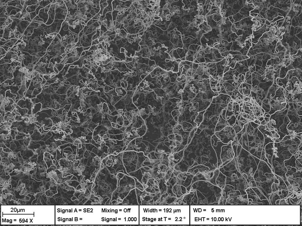
SEM micrograph showing the general morphology of SiNWs grown via SLS mechanism at 1100 °C under Ar–3% H2 atmosphere.
3 Results
3.1 Thermodynamic evaluation of the Au–Si binary alloys
The calculation of phase diagrams reduces the experimental effort required to determine equilibrium conditions in a multicomponent system. The way to resolve such problems is using computational thermodynamics that encompasses the creation of thermodynamic databases based on the Calphad (CALculation of PHAse Diagrams) method and their use in calculation of phase equilibrium with appropriate software Thermocalc developed by Sundman et al. [17].
The equilibrium phases of the Au–Si system are (1) the liquid (L), (2) the face-centered cubic solid solution based on gold 〈Au, fcc〉 and (3) the diamond-type cubic solid solution based on silicon 〈Si, dia〉. We will assume that the condensed phases contain only pure Au and pure Si and that the total pressure P is fixed, as is the temperature T.
Equilibrium between phases can be expressed in one of the two ways: either the total Gibbs free energy of the system is minimized or the chemical potentials (μi) of each component in coexisting phases are equated. It must be pointed out that, in the nanomaterial properties, surface energy cannot be neglected, because of the large ratio surface/volume. Let us first calculate the chemical potentials of silicon in the solid nanowire and in liquid phases.
3.2 The Gibbs energy of a liquid droplet
Let us consider the following transformation:
| (1 − x) 〈Au, fcc〉 + x 〈Si, dia〉 → (solution, liquid) | (1) |
The Gibbs energy of the transformation is given by
| (2) |
By choosing as a standard state for the elements 〈Si, dia〉 and 〈Au, fcc〉:
GL, the molar Gibbs energy of the liquid droplets is the sum of two contributions [18,19]: a volume contribution GLvol, which is the only one taken into account with a macroscopic liquid alloy, and a surface contribution GLsurf which becomes noticeable when the size of the liquid droplet goes down below 100 nm:
| (3) |
The volume contribution is given by the well known thermodynamic expressions:
| (4) |
Since , represent, respectively, the Gibbs energy of fusion of 〈Si, dia〉 and 〈Au, fcc〉. GLxs represents the excess Gibbs energy of mixture given [20] by the Redlich–Kister polynomial expansion:
| (5) |
The surface contribution is given by the general expression
| (6) |
σ(L) and V(L) are the surface tension and the molar volume of the liquid droplet, respectively; r1 and r2 are the main curvature radii of the particle. If the liquid droplet may be considered as a sphere of radius r:
| (7) |
Eq. (6) may be applied to a cylindrical nanowire, in which case r1 = r, radius of the wire and r2 = ∞:
| (8) |
The molar volume V(L) and surface tension σ(L) values were taken from the literature in which the Butler's [21,22] approach has been used for the calculation (Table 1). The surface energies of alloys depend on their composition. There is a large uncertainty in the values of surface energies of solid–liquid interfaces of pure elements and therefore, of their alloys. For the sake of simplicity a linear dependence was assumed between σ(L) of pure Au and of pure Si. Application of such an approximation shows that it has a small effect on the equilibrium states.
Molar volumes and surface tensions of the liquid metals
| σ/J m−2 | Ref | V/m3 mol−1 | Ref | |
| (Au)L | 1.503–2.5 × 10⁻⁴ T | [20] | 8.783 × 10⁻⁶ + 1.427 × 10⁻⁹ T | [24] |
| (Si)L | 1.084–1.3 × 10⁻⁴ T | [20] | 1.003 × 10⁻⁵ + 9.804 × 10⁻¹⁰ T | [24] |
| 〈Si〉dia | 1.299–1.3 × 10⁻⁴ T | [20] | 1.227 × 10⁻⁵ | Calculated |
For Au and Si the partial molar volumes in a solution are nearly equal to those of the pure elements. Thus the molar volume of the liquid alloy V(L) is taken to be a weighted average of molar volumes of the pure liquid elements [20,21]:
GL depends explicitly on T, x and r. For a liquid droplet of radius r:
| (9) |
Fig. 2 shows three curves GL(x) drawn at 1100 °C for r = ∞ (lowest curve), for r = 25 nm (dashed curve) and for r = 5 nm (upper-most curve). The surface contribution increases the Gibbs energy of the droplet, and, as a consequence, decreases its thermodynamic stability.
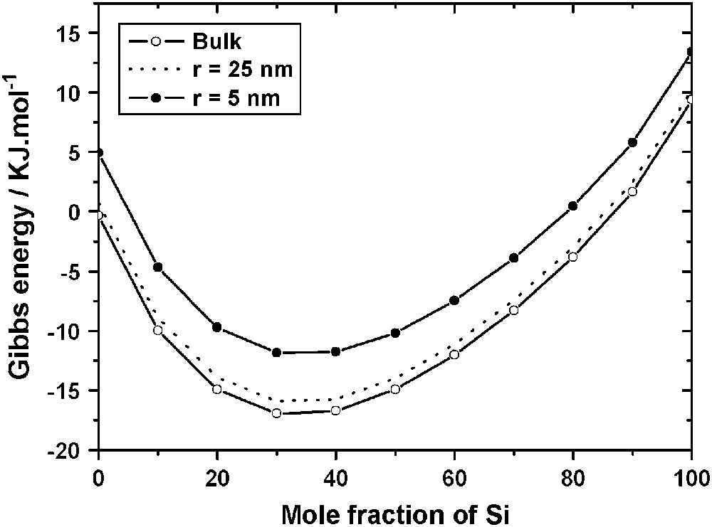
Gibbs energy of Au–Si liquid alloys at 1100 °C for the bulk (r = ∞) and for droplets (r = 5 nm and r = 25 nm).
3.3 The chemical potential of the elements in the liquid
From a curve GL(x) given (Fig. 2), T and r being fixed, it is possible to calculate the chemical potentials μSi, L and μAu, L of the elements Au and Si in the droplet. Introducing activities, instead of molar fractions x, for describing the chemical potential in the real alloy solution and rewriting GL we finally obtained:
| (10) |
| (11) |
| (12) |
Eqs. (11) and (12) may be used with the contributions of GL, namely GLvol and GLsurf, which, are both molar integral Gibbs energy of mixture.
Geometrically, the chemical potentials μAu, L and μSi, L in a given droplet of radius r and composition x, are constructed by drawing the tangent from the point of abscissa x and taking, respectively, the intercept of the tangent to the axis x = 0 (Au axis) and x = 1 (Si axis).
The equilibrium of Si between two phases (namely solid Si and liquid droplet) is expressed by equating the chemical potentials:
| (13) |
- If the solid Si is the Si diamond of the wafer, then and the solubility of the Si bulk in the liquid droplet is obtained by drawing the tangent to the curve issued from the point x = 1, G = 0.
- If the solid Si is the Si nanowire, then and the solubility of the Si nanowire in the liquid droplet is obtained by drawing the tangent to the curve issued from the point x = 1, .
3.4 Chemical potential of silicon in the solid nanowire
The chemical potential of Si in a Si nanowire whose radius is r is given by
| (14) |
aSi, nano, PSi, nano and are the activity of Si in the nanowire, the vapor pressure of Si above the nanowire and the vapor pressure of Si diamond, respectively. aSi, nano > 1 because the nanowire is a metastable form of silicon. σ〈Si〉 and V〈Si〉 are the surface tension and the molar volume of pure solid Si, respectively. Fig. 3 allows the comparison of the solubility of nano- and macroparticles of Si in a liquid alloy: The following conclusions may be drawn:
- • if the liquid alloy is nanometric, the solubility of a nanoparticle of Si is higher than that of bulk Si (S′nano > Snano). The conclusion is the same if the liquid alloy is macroscopic (S′bulk > Sbulk). This conclusion agrees with the accepted statement that the solubility of small particules in a given solvent is higher than the solubility of large particles;
- • however, if the solid Si is nanometric, its solubility is higher in a macroscopic liquid than in a nanometric liquid (S′bulk > S′nano). The conclusion is the same if the solid Si is macroscopic (Sbulk > Snano). This important phenomenon, which deserves attention because of its occurrence in phase diagrams of nanosystems, must be expressed in terms of the nature and properties of the phases involved. The generalization may be made, however, that the solubility of any particle (stable or metastable) is always higher in a macroscopic solvent than in a nanometric solvent.
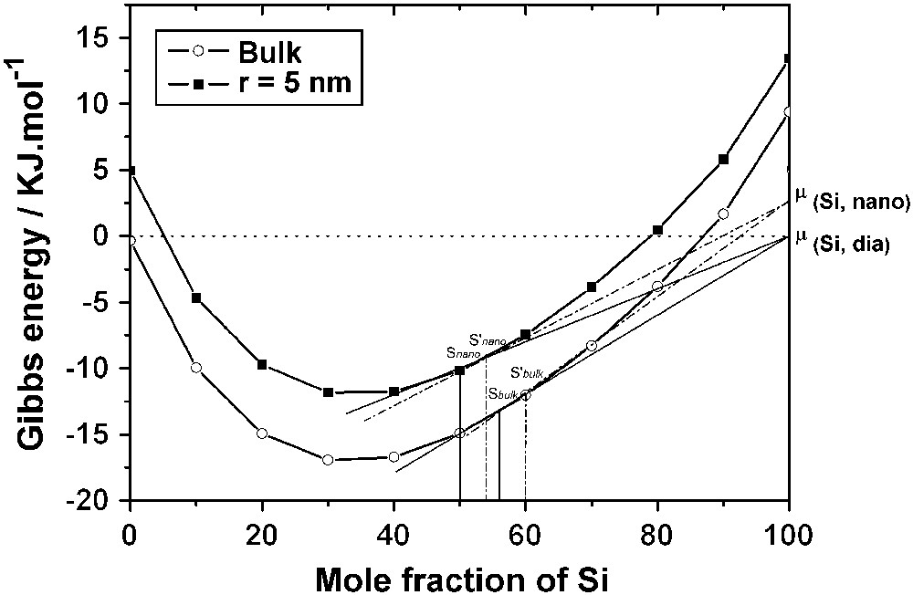
Comparison of the solubility of silicon in a liquid droplet whose radius is 5 nm and in the bulk. Snano and S′nano represent the solubility of 〈Si, dia〉 and 〈Si, nano〉, respectively, in the droplet; Sbulk and S′bulk represent the solubility of 〈Si, dia〉 and 〈Si, nano〉, respectively, in the bulk.
The resolution of Eq. (13) at 1100 °C shows that the solubility of bulk Si in a droplet (r = 5 nm) is Snano = 50 mol% Si compared with Sbulk = 56 mol% Si; the solubility of a nanowire in the same droplet depends on the radius of the nanowire, but it is always observed that (S′bulk > S′nano).
3.5 Phase diagram of the Au–Si system
The calculated phase diagrams are deduced from Eq. (13) and are shown in Fig. 4. The comparative results between bulk and nanosystems show that the trends of the liquidus curves are qualitatively the same, but some differences are evident. The melting temperatures of the pure components decrease with the size of the nanoparticle. The reduction in melting points of the components accompanies a decrease in the eutectic temperature of the system. The crystallization temperature of gold goes down from 1064 °C (r = ∞), to 1043 °C when r = 25 nm and 962 °C when r = 5 nm. For silicon, the temperatures are, respectively, 1414 °C (r = ∞), 1405 °C (r = 25 nm) and 1365 °C (r = 5 nm).
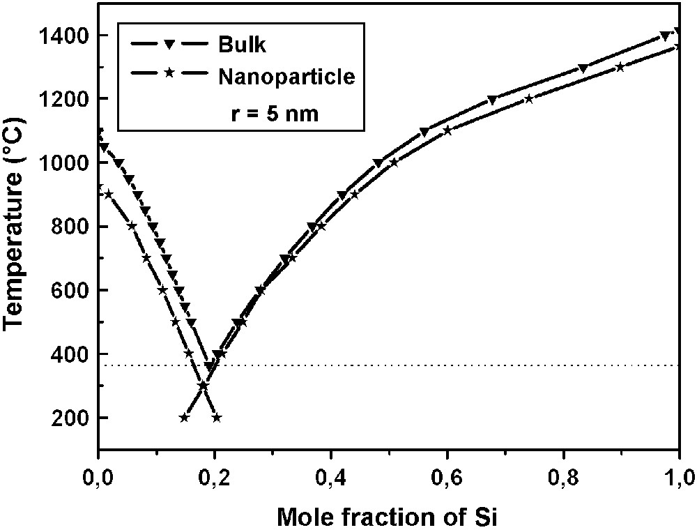
Comparison of the Au–Si phase diagram for the bulk and for droplets (r = 5 nm) in equilibrium with nanocrystals (r = 5 nm).
The conclusion to be drawn from the build up of nanodiagrams is that a gold droplet in equilibrium with the silicon of the wafer is saturated in silicon. Nanowires may be grown from the Au–Si liquid droplets only if the concentration of Si in the liquid is much greater (supersaturation) than that in equilibrium with stable crystals of the same solid (saturation). A first examination of the condensed phases present in the system shows that there is no driving force coming from the wafer to justify any supersaturation of the gold droplet with silicon. It is thus necessary to look towards Si present in the gaseous phase.
3.6 Chemical potentials of gaseous species
In the SLS mechanism, Au, Si and Ar (with or without H2) are the main elements introduced in the synthesis chamber. Another element to be considered is oxygen which arises either from leakage, from degassing of Al2O3 tube or simply from SiO2 which may be native or even intentionally grown by thermal deposition on the substrate. Hence, the silicon species present in the gaseous phase may be either Si, Si2 and Si3 in equilibrium with the solid silicon of the wafer, or SiO in equilibrium with the Si–SiO2 mixture. A rapid analysis of the thermodynamic data shows that the predominating species in the temperature range of interest (800–1400 °C) is SiO. The main equilibrium to be considered is thus the following one:
| 〈Si〉 + 〈SiO2〉 → 2 SiO | (15) |
| (16) |
| (17) |
The coefficients of Eq. (17) are extracted from [23] and are listed in Table 2.
Thermodynamic parameters for the Si–O system
| Δr15G | Δr19G | |
| A | 718 614.749 | 21 951.202 |
| B | −532.537892 | −156.202 |
| C | 24.4690697 | 22.12745 |
| D | 4.99486782 × 10⁻⁴ | −147.0421 × 10⁻⁴ |
| E | 187.917772 × 10⁻⁹ | 1775.6603 × 10−9 |
| F | −923 266.15 | −1 584 843.057 |
The standard state for SiO2 is the solid cristobalite, which is the stable form of silica under the temperature range of interest. As seen above, the standard state for Si is the pure solid silicon 〈Si, dia〉; the standard pressure for gaseous species (O2 and SiO) is P0 = 105 Pa.
If the wafer (aSi = 1) is in equilibrium with the solid cristobalite , the calculated partial pressure of SiO is 4.05 Pa at 1100 °C. When the equilibrium is reached, the chemical potential of silicon is the same in every phase and no more driving force exists to justify the nanowire growth experimentally observed. The explanation of this process has to be researched in the presence of metastable equilibria developed in the system.
The only source of metastability comes from the fact that SiO2 on the wafer is amorphous silica rather than crystallized under the form of stable cristobalite, as it can be easily shown by X-ray diffraction on the silica layers. Actually, all deposited and thermally grown oxides in semiconductor process are amorphous.
The partial pressure of SiO developed by the equilibrium (Eq. (15)) would be higher above the Si/SiO2 (amorphous) couple than above the Si/SiO2 (cristobalite) couple:
| (18) |
aSiO2, am is calculated from the transformation:
| 〈SiO2〉crist → 〈SiO2〉am | (19) |
Δr19G0 is expressed by the same expansion (Eq. (17)) than Δr15G0 and the corresponding coefficients are given in Table 2.
is obtained by extrapolation of towards low temperatures. At 1100 °C:
This difference brings the driving force needed to supersaturate the gold droplets with Si. Gaseous SiO above the wafer, stable with respect to the Si/SiO2 (amorphous) mixture, is thus metastable with respect to the Si/SiO2 (cristobalite) mixture, and the reaction (Eq. (15)) will naturally proceed towards the decomposition of SiO. Without gold droplets, Si and SiO2, resulting from the disproportion reaction 2 SiO → SiO2 + Si, will germinate on the wafer. The gold droplets acting as a catalyst, SiO will decompose on the surface of the droplet and silicon will dissolve until the liquid–gas equilibrium is reached. When the liquid is in equilibrium with the gaseous phase but supersaturated in silicon with respect to the wafer, the precipitation of silicon nanowires will be observed. Amorphous SiO2 synthesized by the disproportion reaction will deposit on the nanowire and on the wafer.
3.7 Calculation of the driving force
From the thermodynamic point of view, the SLS mechanism involved in the growth of silicon nanowires is shown to be the net result of two consecutive reactions: (i) the production of supersaturated SiO (metastable) by reacting amorphous SiO2 coating with the silicon of the wafer and (ii) the disproportion reaction of SiO with formation of Si which supersaturates the gold droplet and SiO2 which deposits on the wafer and on the nanowire. That is why the term SVLS seems more appropriate to describe the nanowires growth than the term SLS often used in the literature, because it takes into accounts the important role of the SiO species into the gaseous phase.
The driving force of the silicon nanowire growth ΔdG is the difference between the chemical potential of the silicon in the droplet in equilibrium with the gaseous phase and that of the silicon wafer:
| (20) |
The ratio is calculated from the equilibrium Si + ½O2 → SiO by taking into account the fact that oxygen pressure, imposed by the system, is constant throughout the whole experiment:
| (21) |
The strength of a model lies in its predictive character. Our model allows foreseeing the minimum radius of the nanowires grown from the supersaturated gold droplets. Indeed, the driving force given by Eq. (21) is used to allow the transformation of stable Sidia, into metastable Sinano. The Gibbs energy of the transformation, depending on the radius of the nanowire, is given by Eq. (8):
| (22) |
At last, Eq. (22) gives the minimum radius of the nanowires:
This calculated value is indeed a minimum one because the available driving force for the nanowire growth depends on the ratio (PSiO nano/am/PSiO dia/am) whereas the energy needed to synthesize a nanowire, given by Eq. (8), increases when r decreases. The minimum size of the nanowire will be obtained when both members of Eq. (22) are equal.
4 Conclusion
In conclusion, the nanowires' growth cannot be explained by the slight modification of the Au–Si phase diagram with the radius of the nanodroplets. An important factor revealed by our research and, heretofore, not given sufficient attention is the issue of a gas phase induced by metastable equilibrium. In the limit where thermodynamic arguments remain valid, it is deduced that the nanowire size limit is in fact imposed by the difference between the chemical potential of the silicon in the gaseous phase and that of the silicon in the wafer. At 1100 °C, temperature commonly used for the growth of nanowires by the SVLS mechanism, the minimum size limit of the first generation of nanowires lies in the 10 nm radius range. The open question remains concerning the nanowire growth from alloy droplets less than 10 nm in size. From a thermodynamic point of view the answer is there is no growth via SVLS mechanism from small particles (radius < 10 nm) of alloy (Au–Si). However, very small size nanowires can also be obtained owing to the existence of the new metastable equilibrium Si nanowire/SiO2 amorphous. The characterization of nanowires continues and will provide further support in determining the size limit of the next generation of nanowires. The results will be published in a future paper. It is therefore a convincing suggestion that the size of nanowires should be further reduced in the second and the third generations.
This work has been supported in part by the ANR-France (contract JC05_46152).