

1 Introduction
The wetting of solid surfaces is an important physical property that is controlled by both the surface energy and the geometrical micro/nanostructure of the surface. The study of wetting properties of a solid surface is crucial for potential applications including hydrophobic interactions, microfluidic devices and self-cleaning surfaces [1–3]. Tailoring the wetting properties of a solid is achieved by controlling the surface termination and roughness. The chemical composition/termination of a surface is tuned by chemical functionalization, while surface roughness is introduced through micro- or nanostructuration of the surface.
The functionalization of hydrogen-terminated silicon (Si) and porous silicon (PSi) surfaces has generated a huge interest, because of the interest of such silicon in modern technology [4–7]. While the primary interest in the surface modification was aimed at preserving the good electronic properties offered by the hydrogen termination, introducing functional groups on the surface allows for designing chemical and biosensors.
The characterization of the wetting properties of hydrogenated and derivatized Si [8–11] and PSi [12,13] surfaces has been addressed in a few independent reports. Water contact angle values comprised between 104 and 110° were measured on hydrogen-terminated Si(111) surface modified with 1-dodecene under thermal [8,11] or photochemical [9] conditions. Water contact angle values of 44° [9] and 48° [8] were reported for acid-terminated Si(111) surfaces, prepared through acid hydrolysis of ester-terminated surfaces. A quite different behavior was observed on hydrogenated PSi surfaces functionalized with 1-undecene (135°) [12] and 1-dodecene (115°) [13] under thermal conditions. Similarly, the water contact angle values of hydrogenated PSi surfaces modified with undecylenic acid vary between 60 and 83° [12,13]. This difference is most likely due to the preparation conditions (surface roughness) of the surfaces investigated in these reports.
In contrast to flat silicon and PSi surfaces, the chemical functionalization of hydrogenated silicon nanowires (SiNWs) surface is investigated only in a few reports. Indeed, the direct reaction of hydrogen-terminated (SiNWs) with 10-N-Boc-amino-dec-1-ene [14,15] or tert-butyl allylcarbamate [16] under UV irradiation was used to introduce – NH2 terminal groups on the nanowires surface for subsequent biomolecule immobilization. A two-step functionalization procedure consisting of chlorination/alkylation of hydrogenated SiNWs was used to introduce alkyl groups onto the surface and impart good stability against oxidation [17–19]. A “clickable” monolayer platform was formed on hydrogen-terminated SiNWs by thermal reaction with α,ω-diyne 1,2-ethanediol dipropiolate. The terminal alkynyl groups were subsequently reacted in a Huisgen 1,3-dipolar cycloaddition reaction with an alkyl azide [20]. Electrografting of hexynoic acid to H-SiNWs resulted in an organic layer terminated with carboxylic moieties used for protein covalent immobilization through amide bond formation [21].
While these reports focused mainly on the chemical functionalization of hydrogenated SiNWs with the aim to passivate the surface against oxidation or to immobilize biomolecules, the wetting properties of the modified H-SiNWs were investigated only in a few reports. Furthermore, the direct reaction of the hydrogenated SiNWs with 1-octadecene or undecylenic acid was not previously reported.
Recently, we have demonstrated that superhydrophobicity can be achieved through the combination of the high surface roughness of silicon [22–27] and silicon oxide [28] nanowires and coating with low surface energy molecules. The SiNWs were prepared by the vapor-liquid-solid (VLS), solid-liquid-solid (SLS) growth mechanisms or via metal-assisted chemical etching. Furthermore, we have shown for the first time that for silicon nanowire substrate of given length and density, the wetting properties can be reversibly switched [22]. The self-cleaning properties of the nanostructured silicon surfaces were furthermore exploited to design Lab On Chip devices for efficient collection of biological particles (proteins, bacterial spores and a viral simulant) using electrowetting on dielectric (EWOD) actuated droplets [29]. Furthermore, the large wetting contrast, superhydrophobic/superhydrophilic, of chemically modified SiNWs was used to study the interaction with biomolecules [30], cells [31] and bacteria [32]. In all these studies, the SiNWs surface was first oxidized and then modified with a low surface energy molecule such as octadecyltrichlorosilane (OTS), 1H,1H,2H,2H-perfluorodecyltrichlorosilane (PFTS) or through C4F8 coating.
Here, we investigate the effect of surface roughness and chemical composition on the wetting properties of silicon-based substrates: crystalline, porous and nanowires. The surface roughness was controlled through porosification of crystalline silicon in HF-based solutions while the chemical composition was varied by the incorporation of different molecules through hydrosilylation reaction under thermal conditions [33–37]. The surface morphology of the resulting surfaces was characterized using scanning electron microscopy (SEM) and atomic force microscopy (AFM). The chemical composition of the surfaces was evaluated using transmission mode Fourier transform infrared (FTIR) spectroscopy and X-ray photoelectron spectroscopy (XPS). The wetting properties of the surfaces were examined using static water contact angle measurements.
2 Experimental part
2.1 Materials
All cleaning (H2O2, 30%; H2SO4, 96%) and etching (HF), (NH4F, 40%) reagents were of VLSI grade and supplied by Merck. All chemicals were reagent grade or higher and were used as received unless otherwise specified. Silver nitrate (AgNO3), dimethylformamide (DMF), 1-octadecene, undecylenic acid, chloroform (CHCl3) and hexane were obtained from Aldrich.
2.1.1 Sample preparation
2.1.1.1 Hydrogen-terminated crystalline silicon
Hydrogen-terminated Si(111) was prepared from shards of silicon (single side polished, n-type, phosphorus-doped, 0.03-0.05 Ω-cm resistivity) by cleaning sequentially in acetone, ethanol and deionized water in an ultrasonic bath, and 3:1 concentrated H2SO4/30%H2O2 at 100 °C for 20 min, followed by copious rinsing with deionized water. The clean surface was immersed in deoxygenated 40% NH4F aqueous solution for 10 min under inert atmosphere, rinsed with deionized water and dried under a stream of nitrogen.
2.1.1.2 Porous silicon
Double side polished (100) oriented p-type silicon wafer (boron-doped, 5-10 Ω-cm resistivity) was first cleaned in 3:1 concentrated H2SO4/30% H2O2 for 20 min at room temperature and then rinsed copiously with Milli-Q water. The clean wafer was immersed in 40% aqueous HF solution for 1 min at room temperature to remove the native oxide. The resulting hydrogen-terminated substrate was electrochemically etched in a 1:1 (v/v) pure ethanol/40% aqueous HF for 5 min at a current density of 10 mA/cm2. After etching, the samples were rinsed with pure ethanol and dried under a stream of dry nitrogen prior to use.
2.1.1.3 Silicon nanowires
Single side polished (100) oriented p-type silicon wafers (boron-doped, 0.009-0.01 Ω-cm resistivity) were sequentially cleaned in acetone, ethanol and deionized water in an ultrasonic bath, and 3:1 concentrated H2SO4/30%H2O2 at 100 °C for 20 min, followed by copious rinsing with deionized water. The clean surface was placed in a sealed Teflon beaker containing HF (5.25 M)/AgNO3 (0.02 M) aqueous solution and heated up to 50 °C for 10 min. The resulting surface was further dipped three times in an aqueous solution of H2O/HCl/HNO3 (1/1/1 in volume) for 2 h at room temperature to remove the electroplated metal [30,38,39].
Safety considerations. The mixture H2SO4/H2O2 (piranha) solution is a strong oxidant. It reacts violently with organic materials. It can cause severe skin burns. It must be handled with extreme care in a well-ventilated fume hood while wearing appropriate chemical safety protection.
HF is a hazardous acid which can result in serious tissue damage if burns were not appropriately treated. Etching of silicon should be performed in a well-ventilated fume hood with appropriate safety considerations: face shield and double-layered nitrile gloves.
2.1.2 Chemical functionalization
The freshly prepared hydrogen-terminated silicon-based substrate was placed under nitrogen in a Schlenk tube containing a deoxygenated neat 1-octadecene or undecylenic acid and allowed to react at 180 °C for 4 h. The excess of unreacted and physisorbed reagent was removed by rinsing, at room temperature, with chloroform. Then, the functionalized surface was rinsed in boiling acetic acid during 5 min followed by a bath of ethanol. Finally, the sample was dried under a gentle stream of nitrogen.
2.1.3 Surface characterization
2.1.3.1 FT-IR Spectroscopy
Transmission FT-IR spectra were recorded using a Perkin Elmer Spectrum 2000 spectrometer at 4 cm−1 resolution. The samples were mounted in a purged sample chamber. Background spectra were obtained using a flat untreated Si(100) wafer that had been dipped in 5% HF aqueous solution to remove the native oxide layer.
2.1.3.2 X-ray photoelectron spectroscopy
X-ray photoelectron spectroscopy (XPS) measurements were performed with an ESCALAB 220 XL spectrometer from vacuum Generators. A monochromatic Al Kα X-ray source (1486.6 eV) was operated in the CAE (constant analyser energy) mode (CAE = 100 eV for survey spectra and CAE = 40 eV for high resolution spectra), using the electromagnetic lens mode. The angle between the incident X-rays and the analyzer is 58°. The detection angle of the photoelectrons is 90°, as referenced to the sample surface.
2.1.3.3 AFM measurements
The samples were imaged with a Dimension 3100 model AFM (Veeco, Santa Barbara, CA) equipped with a Nanoscope IV controller (Digital Instruments) under ambient conditions. Single beam silicon cantilevers (AFM-TM Arrow, Nanoworld) with spring constants of ∼42 N m−1 and resonant frequencies of ∼250 kHz were used. All AFM images were acquired in tapping mode at a constant force of 5-50 pN.
2.1.3.4 Scanning electron microscopy
SEM images were obtained using an electron microscope ULTRA 55 (Zeiss) equipped with a thermal field emission emitter, three different detectors (EsB detector with filter grid, high efficiency In-lens SE detector, Everhart-Thornley secondary electron detector) and an energy dispersive X-ray analysis device (EDX analysis).
2.1.3.5 Contact angle measurements
Water contact angles were measured using a 1 μL droplet of deionized water. We used a remote-computer controlled goniometer system (DIGIDROP by GBX, France) for measuring the contact angles. The accuracy is ± 2°. All measurements were made in ambient atmosphere at room temperature.
3 Results
3.1 Flat silicon Si(111)
The chemical functionalization [4,5,7] and the wetting properties [8–11] of hydrogen-terminated Si(111) surfaces under different conditions have been investigated by several research groups. We have used the thermal approach to functionalize atomically flat hydrogen-terminated Si(111) surface with 1-octadecene or undecylenic acid (Fig. 1). Tapping mode AFM imaging confirms that the hydrosilylation process preserves the surface morphology (atomically flat with easily recognizable Si(111) edge steps) with an average line roughness of 0.165 nm over 6 μm, as shown in Fig. 2.

Schematic illustration of the functionalization process of hydrogen-terminated silicon-based substrates with undecylenic acid or 1-octadecene.
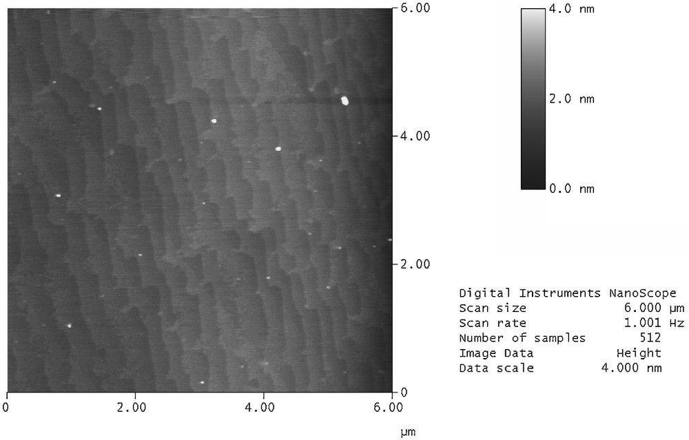
Tapping mode AFM image of crystalline silicon substrate chemically modified with 1-octadecene.
The as-prepared Si(111)-H surface displays a water contact angle of 84° comparable to the literature data [8,9]. After reaction with undecylenic acid at 180 °C for 4 h, the water contact angle decreased to 58°. This value is consistent with a monolayer terminated with COOH groups rather than C = C double although it is not excluded that a small fraction of the monolayer is bonded to the silicon surface through the acid group. The value is slightly higher than 48° reported for an acid-terminated Si(111) prepared by hydrolysis in acid solution of an ester-terminated surface [8] and lower than 65° measured on a surface that has been modified with undecylenic acid in the presence of 0.1% of 2,2,6,6,-tetramethyl-1-piperidinyloxy (TEMPO) [10]. The hydrosilylation reaction of 1-octadecene with Si(111)-H surface under thermal conditions led to a surface with a static contact angle of 105°, in accordance with values reported for surfaces functionalized with 1-alkenes (104-110°) [8,10,11].
3.2 Porous silicon (PSi)
The shape, size, and orientation of the pores generated during the electrochemical etching of silicon wafers are dependent on the current density, electrolyte composition, and dopant type and level. We have used low doped p-type Si(100) and a low current density to generate mesoporous structures. AFM and SEM were used to characterize the porous layer morphology and thickness. Tapping mode AFM image of freshly etched PSi sample shows a smooth surface with statistical rms roughness value in the order of 2.50 nm. AFM imaging did not show significant changes in the topographical characteristics between freshly etched and chemically functionalized samples. SEM top view of the porous surface that has been etched at 10 mA/cm2 for 10 min is shown in Fig. 3a. The image clearly shows average pore sizes below 10 nm. A cross-sectional view (Fig. 3b) shows the branched morphology of the porous layer. Under the conditions that were used, the typical thickness of the porous layer was about 0.6 μm. The porous silicon layer is transparent to wavelengths in the IR region, and spectra can conveniently acquired using transmission FTIR spectroscopy. Fig. 4a exhibits the FTIR spectrum in transmission mode of a hydrogen-terminated PSi surface. It displays typical bands for Si-H stretching modes νSi-H at 2082 and 2110 cm−1, Si-H scissor mode δSi-H2 at 907 cm−1 and Si-Si stretching modes νSi-Si at 628 cm−1. A small peak at 1037 cm−1 due to Si-O-Si stretching mode, resulting most likely from partial oxidation of the reactive Si-H surface bonds upon exposure to ambient air, is also observed. These results are in accordance with those reported in the literature [36,37]. After thermal hydrosilylation reaction between PSi-H and undecylenic acid, new peaks at 2855 and 2924 cm−1 (C-H stretching modes), 1465 (methylene bending modes), 1713 cm−1 (C = O stretching mode) and 3060 cm−1 (νOH) appeared in the FT-IR spectrum (Fig. 4b). A large decrease of νSi-H (2110 cm−1) and δSi-H2 (907 cm−1) intensity was observed, indicating that the reaction took place with silicon-hydride consumption. However, a small increase of νSi-O-Si suggests that a partial oxidation of the surface occurred during the thermal process. The FT-IR results clearly indicate that the thermal reaction between the PSi-H surface and undecylenic acid has successively led to the formation of an organic layer terminated with –COOH terminal groups. The results are similar to those reported in the literature [36,37]. In a similar way, the reaction of hydrogenated porous silicon substrate with 1-octadecene at 180 °C for 4 h led to the formation of an organic layer covalently attached to the surface through SiC bond [37,40]. Additional peaks at 2922 and 1465 cm−1 due to CH stretching and methylene bending modes, respectively of the alkyl chain appeared in the FTIR spectrum (Fig. 4c). Again, a large decrease of νSi-H (2110 cm−1) suggests that the reaction took place with Si-Hx consumption.
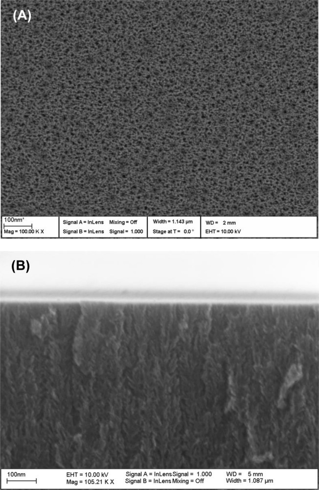
Top (A) and cross-sectional (B) view SEM images of porous silicon.
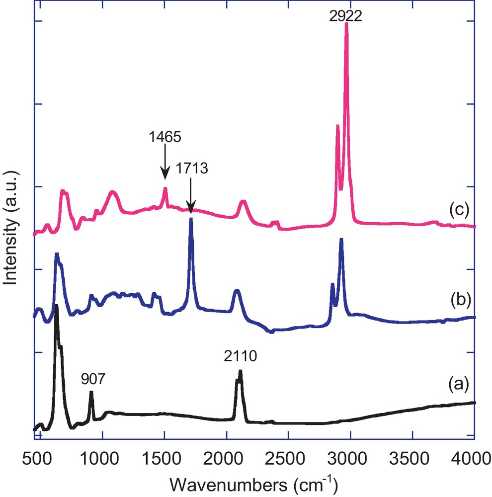
Transmission FTIR spectra of hydrogen-terminated PSi surfaces before (a) and after chemical functionalization with undecylenic acid (b) and 1-octadecene (c).
The wetting properties of the PSi surfaces before and after chemical functionalization were evaluated using static contact angle measurements. The as-prepared PSi surface exhibits a hydrophobic character with a contact angle of 104°, slightly higher than 99° measured on porous silicon with mesopores of 10 to 20 nm in diameter. After functionalization with undecylenic acid under thermal condition, the contact angle decreased to 60°. This value is comparable to that reported for hydrogenated PSi (anodization of p-type Si(100), 7 Ω-cm, in HF/EtOH: 1/1 at a current density of 15 mA/cm2 for 5 min) modified with undecylenic acid under thermal conditions [13]. On the other hand, thermal modification of the hydrogen-terminated PSi surface with 1-octadecene resulted in a significant increase of the static contact angle to a value of 122°, slightly higher to that reported for PSi modified with dodecene (115 ± 5°) [13]. These contact angle values are, however, lower than those reported for PSi surfaces (prepared from p-type Si(100), 0.008 to 0.012 Ω-cm, by anodization at 400 mA/cm2 in HF/EtOH:1/1) modified with undecene (133.5°) or undecylenic acid (83°) under thermal conditions [12]. The difference in the nanotexture of the PSi samples prepared under different conditions may contribute to the observed contact angles.
3.3 Silicon nanowire arrays (SiNWs)
The silicon nanowire arrays investigated in this work are prepared by chemical etching of p-type silicon wafers (boron-doped, 0.009–0.01 Ω-cm resistivity) in HF (5.25 M)/AgNO3 (0.02 M) aqueous solution at 50 °C for 10 min. The technique is easy to carry out and allows the formation of nanostructures on a whole wafer. As shown in SEM images (Fig. 5), dense arrays of silicon nanowires with diameter size in the range of 20 to 80 nm and 2.7 μm in length are formed under these experimental conditions. The top view SEM image (Fig. 5A) shows that the nanowires are stuck to each other to form bundles, giving rise to the formation of pores of 1 to 2 μm in diameter. This phenomenon may be attributed to van der Waals attraction between the nanowires upon drying [31,41]. This phenomenon has previously been highlighted on Ag nanowires grown in highly ordered porous aluminum oxide template after controlled dissolution of the alumina matrix and drying [42]. Alternatively, it was also suggested that some nanowires may be left undetached due to inhomogeneous etching induced by a random Ag particle distribution [43,44]. The high roughness of the surface and the presence of large voids (or pores) limit its AFM imaging.
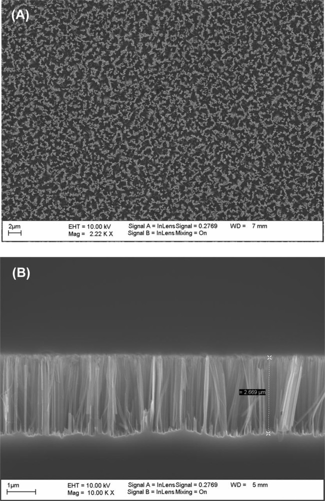
Top (A) and cross-sectional (B) view SEM images of silicon nanowires.
X-ray photoelectron spectroscopy (XPS) was used to analyze the chemical composition of the surface after functionalization (Fig. 6). XPS survey of the as-prepared SiNWs arrays surface shows signals due to silicon Si 2p and Si 2s at 99 and 151 eV, respectively (data not shown). After reaction with 1-octadecene, a significant increase of the carbon signal was observed (Fig. 6a). It is worth to notice that there is no trace of oxygen in the spectrum, suggesting that the hydrosilylation process occurred without any apparent oxidation of the surface. Thermal derivatization of the hydrogenated SiNWs surface with undecylenic acid led to an increase of the carbon signal at 285 eV and appearance of a new peak at 532 eV due to oxygen (O 1s), consistent with an incorporation of the organic molecule onto the surface (Fig. 6b).
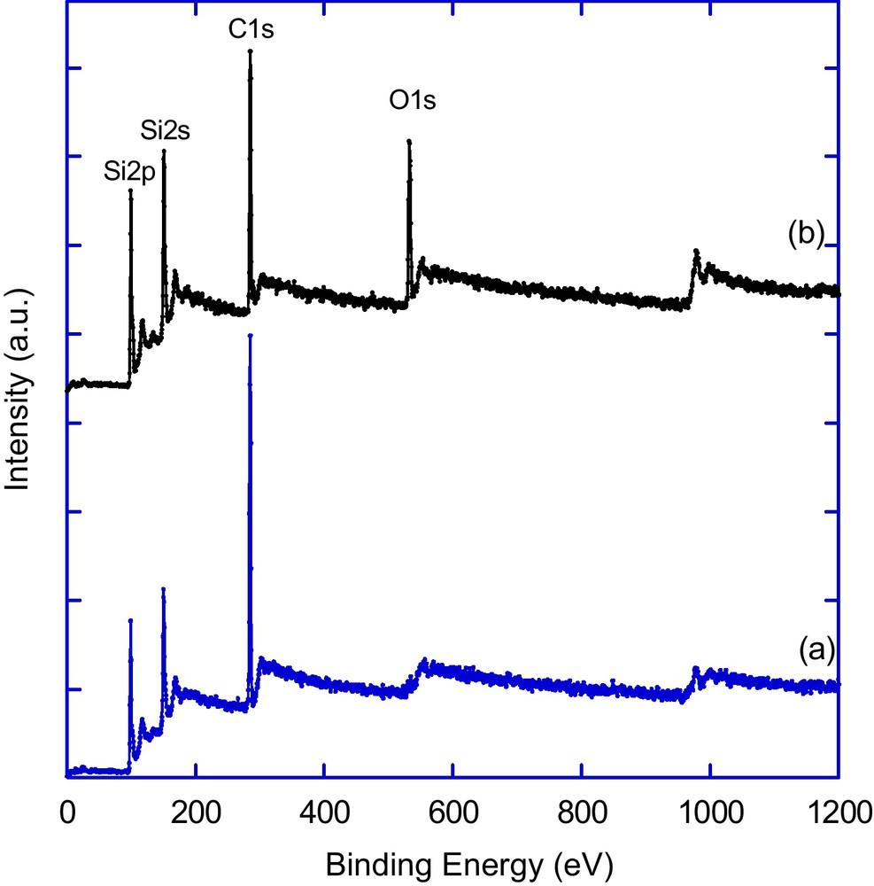
X-ray photoelectron spectroscopy (XPS) survey spectrum of silicon nanowires surface functionalized with 1-octadecene (a) and undecylenic acid (b).
The high resolution XPS spectrum of the C1s of the SiNWs surface functionalized with 1-octadecene consists of two peaks at around 284.0 eV (C-Si) and 285.1 eV (C-C and C-H), characteristic of the alkyl chain (Fig. 7a). The carbon peak of the surface derivatized with undecylenic acid can be deconvoluted into four peaks, ranging from low to high binding energies, as follows:
- • a peak at 283.9 eV for carbon atoms that are covalently bonded to silicon (C-Si);
- • a peak at 285.0 eV for carbons in the aliphatic chain (C-C and C-H);
- • a peak at 286.3 eV for α-carbons adjacent to the carbonyl atoms;
- • a peak at 289.6 eV for the carbonyl carbon atoms (Fig. 7b).
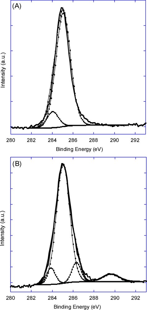
High resolution X-ray photoelectron spectroscopy (XPS) spectra of C1s of silicon nanowires surface functionalized with 1-octadecene (A) and undecylenic acid (B).
The results are in accordance with those reported on hydrogenated SiNWs chemically functionalized with an alkyl chain [17,18], and hydrogenated flat silicon [45] and porous silicon surfaces modified with undecylenic acid. The absence of a peak at 103 eV in the high resolution spectrum of Si2p confirms that the hydrosilylation reaction took place without oxidation of the surface.
Water contact angle measurements were used to follow the changes of the wetting properties of the surface. The water contact angles of the hydrogenated SiNWs arrays before and after thermal hydrosilylation are displayed in Table 1. The hydrogen-terminated SiNWs arrays exhibits a water contact angle of 137°, much higher than that measured on a flat hydrogenated silicon substrate (84°). After functionalization with undecylenic acid at 180 °C for 4 h, the surface remains hydrophobic with a contact angle of 124°. This value is still remains higher than those measured on flat and porous silicon surfaces modified with the same molecule. The water contact angle increased to 160° after thermal treatment of the hydrogenated SiNWs arrays with 1-octadecene. This treatment confers a superhydrophobic character to the surface with a rolling ball effect. Indeed, by tilting the substrate (< 5°), the droplet rolls off the surface.
Water contact angle of the as-prepared, hydrogen-terminated, substrates before and after functionalization with undecylenic acid or 1-octadecene.
| Contact angle (± 2°) | Rms (nm) | H | COOH | C18 |
| Si(111) | 0.165 | 84 | 58 | 105 |
| PSi | 2.50 | 104 | 60 | 122 |
| SiNWs | – | 137 | 124 | 160 |
4 Discussion
The wetting properties of a surface are determined by the contact angle (CA) between the liquid and the solid surface. It depends on the surface nature (chemical composition, termination, roughness, …) and the nature of interfacial surface tension (solid-liquid-vapor). When a liquid droplet is placed on perfectly smooth and chemically homogeneous surface, the CA is described by the Young's relation and is called the Young's contact angle, θ [46].
| (1) |
In practice, a surface always displays structural defects or roughness as well as chemical heterogeneities. In that case, the CA between the liquid and the surface is described by the apparent contact angle θ*. The wetting properties of rough surfaces are explained by two well-established models, attributed to Wenzel [47], and Cassie and Baxter [48]. In the Wenzel state, the liquid droplet fills up the rough surface, leading to a fully wetted contact. The apparent water contact angle θ* is then expressed by:
| (2) |
In the Cassie and Baxter configuration, it is proposed that the liquid forms a line of contact on the rough surface with air trapped below the contact line so that the liquid at the interface contacts both the solid and the air. The relation between apparent and Young angles on such a composite surface is given by Eq. (3), where Φs is the solid-liquid contacting-surface fraction.
| (3) |
The results in Table 1 indicate that for a given coating, the contact angle increases when the surface roughness is increased, except for acid termination. Moreover, the water contact angle increase is more pronounced when the surface roughness becomes important. It is to be noted that for SiNWs, coating with a low surface energy molecule (octadecene) confers a superhydrophobic character to the surface. On the one hand, it is well-known that in the Wenzel state, the surface becomes more hydrophilic as the surface roughness increases in the hydrophilic regime (0°< θ < 90°). This is not the case for the SiNWs modified with undecylenic acid. Indeed, the SiNWs surface functionalized with undecylenic acid displays a water contact angle of 124°. The hydrophobic nature of the surface cannot be explained with the Wenzel state. On the other hand, the high contact angle measured on SiNWs surface modified with a low surface energy molecule (octadecene) may be explained by invoking the Cassie-Baxter wetting state where water droplets sit on top of the nanowires. This model is valid when the water CA on a smooth surface of the same material is higher than 90° (a water CA of 105° was measured on flat silicon surface functionalized with 1-octadecene). The result is in accordance with a decrease of the solid fraction in contact with water upon silicon etching (increase of surface roughness) and indicates that the achievement of superhydrophobicity is mainly dominated by the air trapped within the nanowires.
5 Conclusions
Control of surface wettability of silicon-based substrates was achieved through the combination of surface roughness and chemical functionalization. The increase of surface roughness combined with coating with low surface energy induced by surface modification ensures air trapping between the substrate and the liquid droplets, necessary to achieve superhydrophobicity. Lowering the contact area between a surface and an aqueous solution will have a dip impact on the interfacial chemical and biochemical reactions. For example, the chemical transformation or coupling of an acid terminal group commonly carried out in aqueous solutions will be hindered on silicon nanowires. The potential of porous silicon and silicon nanowire structures are currently investigated in our laboratory for potential applications in discrete microfluidics i.e. electrowetting actuation mode of liquid droplets.
Acknowledgements
The Direction Générale de l’Armement (DGA), the Centre National de la Recherche Scientifique (CNRS) and the Nord-Pas-de-Calais region are gratefully acknowledged for financial support.