

1 Introduction
During the last decades, low-dimensional materials have shown a wide range of applications in various fields. A great deal of interest in one-dimensional nanostructures, such as nanotubes, nanowires, nanorods, and nanobelts has emerged since size effects result in modified or novel properties that open a new range of electronic, optical, and mechanical nanodevices [1–4]. Since quantum wire effect and the light-emitting properties [5,6] of porous Si (PSi) have been evidenced, semiconductor porous etching became a key route in the field of direct material nanostructuring. There are numerous physical and chemical techniques to produce pores: deposition from colloidal suspensions (by dipcoating, spincoating, or “smearing”), MOCVD (metalorganic chemical vapor deposition), “spark process”, plasma etching, hydrothermal synthesis, sol–gel techniques, deposition from the vapor phase, chemical bath deposition, electrodeposition and (electro)chemical etching… However, the last is particularly interesting since electrochemical methods are cost effective and give latitude for the surface geometry. In this review, we will therefore focus on anodic porous etching of semiconductors. After a brief history relating chronologically the main evolutions of the field, the principles of semiconductor etching will be considered. The mechanisms of porous etching will then be developed while the influence of the key parameters on the pore morphology will be described in a following section. The outlook will focus on the applications of such films.
Since this review article cannot be exhaustive, the reader is invited to refer to books, other review articles and conference proceedings' volumes (e.g. International Conference on Porous Semiconductor Science and Technology or dedicated Symposia of the Electrochemical Society Meetings) in order to find detailed and precise information about physics of semiconductors, electrochemistry of nanomaterials and other fields (see e.g. Refs. [7–16]).
2 History
Anodic porous etching has firstly been shown by Uhlir at Bell Labs in 1956 onto Si and Ge [17]. Localized dissolution of p- and n-type materials was demonstrated and some interesting mechanistic aspects were proposed. After this first paper, other studies have reported the formation of a matte black, brown or red layer onto Si after anodic treatment in HF containing solutions [18,19]. At this time “pitting”, “localized dissolution” or “etch channels” are the preferred terms. It was Watanabe, in 1971, who initiated the use of the word “porous” [20,21]. Although pore formation onto silicon was rigorously investigated, it was not a field of intense activity before the 1990s. It is indeed the discovery of the quantum size effect and the visible light-emitting properties respectively, by Lehmann and Canham [5,6] in 1990, of anodic PSi, evidenced, respectively, by Canham and Lehmann [5,6] in 1990, that has shown to the scientific community the fundamental interest and the potential applications of such layers. As Helmut Föll said “Canham has moved porous layers from laboratory curiosity to a scientific field”. Later in the decade other valuable properties of PSi have been reported. Although silicon is neither biocompatible nor explosive, it has been shown that PSi is both bioactive [22] and it exhibits explosive properties [23–25]. Micro-, meso- and also macropores (IUPAC's pore geometry classification is given in Section 4.1), exhibiting various morphologies and specific area as large as 600 m2 cm−3 [26], have been grown onto p- and n-type silicon with different crystallographic orientations. All these findings have lead to a great deal of interest for the “new” field and further applications were brought to light for PSi. Although some dispersed works were carried out before, it is during the nineties that many studies have targeted the porous etching of other semiconductors (III–V, II–VI and IV groups). Due to their evident optical properties for fast electronic devices, III–V semiconductors such as GaAs, InP and GaP were intensively studied. Krumme and Straumanis [27] have firstly reported crystallographic oriented etch tunnels in n-GaAs after anodic polarization in both acidic and alkaline solutions. Kohl et al. [28] have investigated, in 1983, the photoelectrochemical oxidation of n-GaAs and n-InP in halogenide acids. They reported the formation of deep and numerous pits in HCl for high applied current densities (j). Faktor has also reported channel formation in GaAs [29] and Beale et al. [30] described the porous etching of n-GaAs. Finally Schmuki et al. [31] have evidenced green photoluminescence of GaAs after porosification in HCl. Although Kohl et al. [28] firstly reported InP porous photoetching, it is Takizawa et al. [32], in 1994, who gave a detailed description of the pore formation onto this material. They identified pillars perpendicular to surface for (111)-oriented surfaces while 〈111〉B oriented channels were formed onto (100) surfaces (see Section 4.3.1 for details on this notation). Additionally, they reported a blue shift of the photoluminescence features (ca. 30 meV), ascribed to a quantum size effect. It was Chase and Holt [33] in 1972, then Belogorokhov et al. [34] in 1994 and finally Erné et al. [35] in 1996 who pioneered the porosification of GaP. Attempts to porosify other III–V semiconductors have also been reported. However, these materials were less investigated. Porous photoelectrochemical etching of GaN has been observed [36,37] and a kind of porous layer has been grown onto InSb by Schmuki et al. in 2003 [38] and Borini et al. have evidenced pore formation onto GaSb in HCl [39].
II–VI semiconductors are, with silicon, the ones for which the origin of pore formation was questioned first. Such materials were intensively investigated in view of photoelectrochemical solar cell applications. It was found that anodic polarizations induced extreme surface roughening (the word “porous” was not –at this time– explicitly used) and improved the photoconversion efficiency. Porous etching of II–VI materials was performed under illumination for n-type or in the dark for p-type materials. It was successively reported for n-CdSe [40], n-CdSexTe1−x [41], n-CdS [42], n-CdTe [43], p-CdTe [44], p-Cd1−xZnxTe [45], p-ZnTe [46]. Since improvement of the quantum efficiency was initially targeted by these studies, the layers were not described from the pore formation point of view. Information such as the pore depth is then missing. However, these layers exhibit many similarities to those observed onto Si.
Except Si, group IV elemental or alloyed semiconductors were less investigated. In fact, Ge was made porous simultaneously to Si by Uhlir [17] and later by Miyazaki et al. [47]. Si1−xGex alloys were also made porous [48,49] but the studies have mainly focused on the photoluminescent properties and little information about the pore morphology is given. The SiC polytypes (3C–, 6H– and 4H–SiC) are the second family of IV–IV compounds that have been porosified [50,51]. They have shown potential use as a bright blue light-emitting diode [52]. Polycrystalline [53] and amorphous [54,55] silicon can also be porosified in HF. However, for polysilicon the etching rate depends on the crystal orientation and is enhanced at grain boundaries. The result is an irregular etching front and non-anodized silicon grains can remain in the porous matrix [56]. Although it is not a semiconductor, it is worthy to mention that porous silica can be grown by high voltage anodic treatment of silicon in diluted fluoride acidic solutions [57]. Under adequate conditions, very nice honeycomb-like SiO2 microstructures could be formed [58]. In spite of its wide band gap, boron or phosphorus doped diamond exhibits semiconductive properties. Recently Takasu et al. have reported the catalytic formation of nanochannels in the surface layers of boron-doped diamond by metal nanoparticles under a H2 and N2 stream at 900 °C [59]. However, this physical technique falls outside the scope of the present review.
Similarly to self-organized porous alumina [60], one can also anodically form porous semiconductive oxide films onto valve metals such as TiO2 [61,62] or WO3 [63]. For an extended view of such surface structuring methods, the reader should refer to the review given in Ref. [64].
3 Pore formation
As mentioned in Section 1, there are numerous physical and chemical methods to produce porous semiconductors. Among these techniques, chemical and electrochemical techniques exhibit two main advantages: they are cost effective and allow three-dimensional processing. It is why semiconductor anodic porous etching is the most investigated and used method nowadays. In the following, we report all the wet etching techniques that are known for semiconductors. Obviously electrochemical techniques such as Ge deposition through a silica sphere matrix [61] resulting in a porous structure run out of the scope of the present paper since we want to focus on direct etching techniques.
3.1 Wet etching of semiconductors
Wet etching of semiconductors is basically a material dissolution that can proceed via several mechanisms: chemical, electroless, photochemical, anodic or cathodic etching. Chemical etching is not potential dependent since it does not require any free carriers. It is performed without any external polarization. Conversely, electroless, photochemical, anodic and cathodic dissolutions are potential dependent and are therefore referred to electrochemical processes. In these cases free charge carriers are required in the surface bonds. Electrons are involved in cathodic decomposition while holes are supplied by an oxidizing agent in the case of electroless dissolution, by absorption of a photon in photochemical processes while an external circuit is used during anodic etching. In all cases a competition between dissolution phenomena and oxide formation can occur. Depending on the stability of the as-formed oxide, the passive properties of the film may indeed hamper or stop the etching process. Furthermore, in some pore formation models, oxide growth and dissolution phenomena have been considered as key parameters to understand the localized dissolution processes.
3.1.1 Chemical etching
During the chemical etching a simultaneous bond exchange proceeds between undissociated molecules in the solution and the surface atoms. Chemical bonds between the surface atoms and the bulk atoms are broken while new bonds are formed with the reactants: surface atoms thus move to the solution. Such phenomena are not potential dependent. Both anisotropic and isotropic silicon chemical etching are widely used in microelectronics. Etching in alkaline aqueous solutions containing inorganic (LiOH, NaOH, KOH, RbOH, CsOH, or NH4OH) or organic (ethylenediamine, hydrazin, tetramethyl ammonium hydroxide, choline, and amine gallates) compounds leads to anisotropic Si dissolution in which OH− and H2O are the active species. Conversely, isotropic Si etching is achieved in acidic media that contain fluoride ions (HF). Chemical etching of III–V semiconductors such as GaAs and InP (see Eq. (1)) is achieved using bifunctional species that can be either symmetrical (H2O2, Cl2, Br2, and I2) or asymmetrical (ClO−, HCl, and HBr) [65]. II–VI materials can also be chemically etched. No pore formation onto semiconductors has been reported using such etching mechanism.
3.1.2 Electroless etching (or “stain” etching)
Because bonding states correspond to the valence band of the semiconductors [65,66], it is necessary to supply holes to the semiconductor surface in order to achieve electrochemical etching of the material. In the case of electroless or “stain” etching, holes are created by reducing an oxidizing agent via the valence band of the semiconductor. The oxidant extracts electrons from the solid, i.e. injects holes into the band. Such a dissolution process takes place onto both p- and n-type semiconductors but the electron acceptor levels of the redox couple must have an energy distribution overlapping with the valence band of the semiconductor. For instance, GaAs can be dissolved in Ce4+ containing solutions:
| (2a) |
| (2b) |
3.1.3 Photochemical etching
Photochemical etching (or photoetching) is an electrochemical process in which the semiconductor surface is dissolved under illumination without external bias. In this case, photons induce the creation of electron/hole pairs that will further be involved in the electrochemical dissolution. This technique has initially been used to reveal crystal imperfections or to perform selective material etching. Porous photoetching has firstly been reported onto Si by Noguchi and Suemune [72]. The porosification process is initiated by hole generation located at the surface Si–H bond. The overall simplified process is commonly described (Eq. (3)) by the hole initiation followed by the F− reaction with Si [6,73].
| (3) |
3.1.4 Anodic dissolution
Basically we just need to place the material we want to porosify in a beaker, add a counter electrode (e.g. Pt wire or mesh) and connect both electrodes to a current/voltage source to strongly anodize the semiconductor surface. In reality some refinements are requested to tailor the nanostructures. The semiconductor/electrolyte junction that is established as soon as the semiconductor is immersed in the solution must be taken into account since the charge distribution at the interface controls the etching phenomena. According to the model proposed by Gerischer [74–76], the energetic description of the semiconductor/electrolyte interface is based on Schottky's model [77] that depicts the semiconductor/metal junction combined with the Marcus theory of surface chemistry [78,79]. For a complete description the reader can refer to numerous articles and books (see for e.g.: Refs. [7,8,66]). According to the purpose of this review, the main information to remember is the establishment of a space charge layer (SCL) close to the surface that is either in accumulation or depletion of majority carriers. When depletion conditions are established there is formation of an energetic barrier: the “Schottky” barrier. Both width of the SCL (WSCL) and barrier height (USb) are voltage dependent. The consequence is that the semiconductor/electrolyte interface behaves like a diode. Depending on the type of doping and the applied potential, the junction is either under blocking or a passing situation. Anodic etching occurs therefore onto p-type materials in the dark (forward bias) while illumination is necessary for an n-type semiconductor (reverse bias). Nevertheless, it will be shown later (Section 4) that porous etching can proceed even if these conditions are not strictly respected. Note that in some cases, chemical, electroless and anodic etching phenomena can take place simultaneously or successively.
3.1.5 Cathodic etching (or cathodic decomposition)
Although it is not used in industrial processes, etching of II–VI [80] and III–V [81] semiconductors can be performed under cathodic polarization. The so-called cathodic decomposition proceeds after adsorption of atomic hydrogen onto the surface and competes against further H2 formation. The decomposition yield is, however, very low since hydrogen evolution is the main reaction. The two-step mechanism is illustrated for n-InP in acidic media in Eqs. (4). This wet etching method does not yield porous structures.
| (4a) |
| (4b) |
| (4b′) |
3.2 Pore formation models
Pore formation mechanisms onto semiconductors have firstly and mainly been studied on single-crystalline silicon. The first model has been proposed in 1972 by Theunissen [82]. It was before the discovery of the visible light-emitting properties of PSi. After 1990, many studies have targeted the formation of porous layers onto other semiconductors but few mechanistic considerations were proposed and the models used to describe the pore formation onto silicon were applied to all semiconductors. Although the pore formation mechanism is still disputable, there are experimental facts that have revealed the main parameters to achieve various and controlled pore morphologies. It is now evident that applied current or voltage, crystal orientation, doping type and density, electrolyte composition, solvent nature, surface defects, illumination, can strongly influence the porous etching. It is also clear that the pore formation process can be split into two steps: initiation and growth.
3.2.1 Pore initiation
While numerous models tackle the way in which pores propagate, the origin of nucleation is often not as deeply examined. Many studies treat pore initiation as a random phenomenon (see e.g. Refs. [30,83,84]): localized dissolution occurs at surface inhomogeneities inducing an enhancement of the current flow at the interface. In regions of locally high current density preferential attack occurs, resulting in the formation of small depressions. According to Zhang [83] pores nucleate at surface defect locations. A theoretical model of interactions between intrinsic point defects and impurities in the near-surface region of semiconductors during pore formation was later proposed [85]. It was shown that a redistribution of defects and the formation of areas with different concentrations of vacancy-type defects might be the reason for the formation of porous structures. This idea was also supported by Schmuki et al. reporting preferential pore formation at surface defects intentionally created by Si2+ focused ion beam bombardment onto n-type GaAs and Si substrates [86,87]. Conversely, in situ scanning tunneling microscope studies carried out in KOH have shown that surface pitting does occur independently of atomic defects at the initial stages [88]. This tends to rule out surface defects or inhomogeneities as arguments for pore initiation. The same authors have therefore proposed that pore initiation takes place where hydrogen incorporation generates H-related defects [89]. An analytical prediction method based on the pioneering work of Mullins and Sekerka [90] has also been used to mathematically treat pore nucleation as the instability of a planar surface to small perturbations. Kang and Jorné [91] have then used the linear stability to explore pore formation onto n-Si while Chazalviel et al. [92] have looked at amorphous and crystalline p-Si. Finally pore initiation sites can be intentionally positioned by photolithographic processes. The nucleation takes place at inverted four-sided pyramidal pits created by anisotropic etching in KOH [93] (Figs. 1b and 10).

Scanning electron microscopy (SEM) pictures of n-Si (100) etched in HF. The current density was kept constant by adjusting the backside illumination. Top: a random pattern of macropores. Bottom: pore growth was induced by a square pattern of pits produced by standard lithography and subsequent alkaline etching (inset upper right) (from Ref. [104]).

Pore density vs. silicon electrode doping density for PSi layers of different size regimes. The mesopore formation current (in mA cm−2) is indicated in the legend [175].
3.2.2 Pore growth
Contrarily to pore nucleation, mechanistic considerations about pore propagation have led to numerous concepts. Chazalviel [94] has distinguished three different approaches: “chemical”, “physical” and “simulation”.
In the “chemical” approaches, the silicon dissolution enhancement at the pore tip is ascribed to a sort of autocatalytic effect. Unagami [95] had firstly proposed that localized dissolution of p-type silicon was due to the divalent and the tetravalent reactions of silicon with HF, without the disproportionation reaction. The dissolution of the walls is hindered by a layer of silicic acid. Parkhutik et al. [96] have suggested a model based on the mechanisms of porous oxide growth onto metals [97]. It uses the concept of the so-called virtual passive layer. Two competitive processes take place simultaneously during the pore growth: the formation of a passive oxide layer at the bottom of each pore and the electrochemical dissolution of the oxide. The parameter determining the morphology of the porous films is the rate of electric-field-enhanced dissolution of the electrode material at pore tips. Depending on its value, pores with different morphologies may be formed. In situ infrared spectroscopy investigations of porous etching of p-Si in HF [98,99] have nevertheless detected an oxide submonolayer only for dilute HF or HF-free electrolytes. This tends to weaken such models.
Kooij and Vanmaekelbergh [100] have suggested a model assuming that the chemical oxidation of an Si(II) intermediate to an Si(IV) product, which is accompanied by the formation of an H2 molecule, is catalyzed by a mobile Si(I) dissolution intermediate. Based on chemical kinetics, the authors propose a mechanism to explain the pore formation by anodic etching. In a similar approach Soares et al. [101] have proposed that SiF could also play a catalytic role in the localized dissolution process. The surface is heterogeneously covered by Si–H and activated Si–F bonds. Electrons are injected from H2 to Si–H bonds and are transferred to Si–F sites where the dissolution rate is increased. The spatial distribution induces therefore the localized etching. Again such reaction intermediates have not yet been shown.
Voltage oscillation can be observed during galvanic porous etching. Föll et al. [102] have proposed a model to explain such oscillations (Fig. 4). In the current “burst” model, local current flows start as soon as the local field strength is high enough: the current “bursts”. They induce direct Si dissolution or oxidation and stop. The oxide is then chemically dissolved and the cycle starts again. Since the Si exhibits a high reactivity just after dissolution, the next current “burst” will likely take place at the same locations. However the H-termination induces a surface passivation and hampers further “bursts” until it reaches a situation similar to the one before the first event. The H-termination is thus the main synchronizing force because it correlates with the nucleation phenomena. The second reason for the phase locking between pores at high pore density is the overlapping of the space charge regions surrounding each pore. This model has been extended to III–V semiconductors.
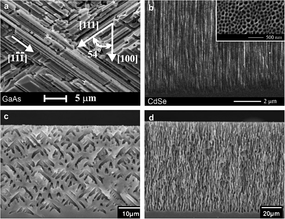
SEM cross-sections of CO and CLO pores grown onto (a) GaAs in HCl, (b) CdSe in NaCl and (c, d) in HF/DMSO (from Refs. [155,197,198]).
The “physical” theories consider the semiconducting properties of the electrode to explain the pore formation. It is therefore easy to extrapolate such models to other semiconductors. As described in the previous section, the electrochemical dissolution of silicon involves the transfer of several charges (between 2 and 4) but it is generally agreed that the first step (hole supply to the surface) is the rate-limiting step during the porous etching process [103]. Hole collection at the surface is therefore the crucial point to understand the pore growth. All these models consider the space charge layer configuration or the electric field at the interface. In some cases, it is also necessary to treat separately n- and p-Si. Theunissen [82] has firstly proposed a model to explain “etch channel” formation into n-Si. He assumed that the channel elongation occurs at locations exhibiting a lower breakdown voltage of the depletion layer. Following the same approach, Beale et al. [30] proposed a more detailed theory. Due to the low resistivity of the electrolyte relative to the fully depleted PSi, the current flows preferentially down the electrolyte. The Si dissolution is therefore confined in the pore apex. The mechanism by which current flows across the Schottky barrier is dependent on the doping level. For highly doped Si, charge transfer through the junction proceeds by direct or Zener tunneling whereas thermoionic emission takes place for low-doped silicon. Zhang [83] and Searson [84] have also proposed a mechanism based on the modifications of the SCL in the porous region. By solving the three-dimensional Poisson's equation for a semispherical pore tip, the SCL is found to be thinner at the pore apex and the electric field is enhanced. Hole supply and charge transfer through the interface are therefore favored at the surface located in the pore tip. Additionally there is an overlapping of the SCL in the pore walls that leads to a full depletion: the pore sides are passivated.
There is now reasonable agreement on the formation of macroporous silicon on n-Si. In the dark, pore elongation results from reverse breakdown of the depletion layer at the pore vertex. The pore wall thickness is controlled by WSCL. The ratio between the applied and the electropolishing currents drives the pore diameter and the porosity. The understanding of these mechanisms has enabled the growth of well-defined and well-controlled macropore structures. A very good example is given by Lehmann [104] who has fabricated perfectly tubular pores onto n-Si under backside illumination (see Fig. 1). The holes diffuse to the interface until they are captured by the depletion layer which accelerates them toward the pore bottoms. Such porous structures show that the pore morphology depends on the hole generation mechanism; branched pores with sharp tips form if holes are generated by breakdown, whereas hole generation by illumination produces unbranched pores with larger tip radii. This was confirmed by Kang and Jorné [105]. For these authors, PSi is formed when the dissolution process is limited by the hole supply and the density of PSi is both material- and process-dependent. Note that Lehmann and Rönnebeck do not fully agree on this point [106].
According to the “physical” models related before, micropore formation onto p-Si is a surprising result since contrarily to n-type semiconductors, p-type electrodes are under forward bias when anodic potentials are applied. Various mechanisms have then been proposed leading to a controversy in the literature. Similarly to a previous work [30], Hérino et al. [107] have proposed that for p-Si, the hole transfer to the interface occurs through a thinner depletion layer located at the pore vertex. Lehmann and Gösele [6] have attributed the micropore formation onto p-Si to hole depletion in the surface vicinity due to quantum confinement in the pore walls (this is also true for n-Si).
Macropores onto p-Si have firstly been reported by Chazalviel et al. [108]. They came up with a model based on resistivity considerations. The authors consider that macropores grow onto p-Si if the semiconductor's resistivity is higher than the electrolyte's one. A resistivity threshold for the p-Si is therefore suggested to get macroporous etching. The same year, Lévy-Clément and Ponomarev [109] have investigated the macropore formation onto p-Si in non-aqueous solvents and the influence of water addition. According to Kohl et al. [110,111] the electrochemical etching of silicon in anhydrous HF solution leads to the formation of Si–F bonds rather than Si–OH. Since the Si–F bonds are strongly polarized and hence more reactive, further electrochemical Si dissolution processes are faster in non-aqueous solutions than in water. Hole diffusion over the surface is then hindered and charge consumption occurs mainly at the pore tip. They concluded that a passivation by absorption of organic molecules was responsible for macropore formation. One year later, Lehmann and Rönnebeck [106] reported results invalidating both previous models. They proposed a model built on the charge transfer mechanism through a Schottky barrier. After geometrical considerations, the barrier width is found thinner at the pore apex. For low doping concentration, this leads to a local increase of the diffusion current and to a depletion of holes in the pore sides.
In parallel to the “chemical” and “physical” approaches, numerous models are based on random-walk simulations. Most of these theories consider the diffusion of holes from the bulk to the Si/electrolyte interface. This is the case for the first reported model [112]. Based on the diffusion-limited aggregate theory [113], Smith et al. [112] have suggested a model where the rate of pore growth is limited by the diffusion of necessary reactants, holes or electrochemical species, to the interface. Their computer calculations exhibit a qualitative agreement with observations carried out by transmission electron microscopy (TEM) onto p- and n-type PSi. Later Yan and Hu [114] have modeled the interfacial dynamics that drives the porous etching using a two-dimensional two-component resistor network. The ratio of the resistances of the two networks is used to simulate the progression of the interface according to a stochastic dynamics that involves localized currents. Erlebacher et al. [115] have performed a Monte–Carlo calculation of the pore nucleation and propagation. This approach has then been developed by John and Singh [116]. They have reported the diffusion-induced nucleation concept. This two-dimensional simulation is based on two primary processes: the initial etching process is controlled by hole diffusion to the surface and further pore elongation is described with a finite termination probability. In the previous paragraph about pore initiation, a series of models built on the linear stability analysis initially introduced by Mullins and Sekerka [90] have been mentioned. Both Kang and Jorné [91] and Chazalviel et al. [94] theories have described the pore elongation process using this calculating method. In order to establish their model based on the catalytic role of SiF species, Soares et al. [101] have used a semiempirical Hartree–Fock calculation to demonstrate the spatially variable dissolution of silicon. Although these computational or analytical methods are quite efficient to describe the various morphologies of PSi layers, they are powerful as soon as the chemical or physical aspects are correctly stated.
Although a competition between the “chemical” and “physical” approaches exists, there is an agreement on the two-step description of the process. It seems that “chemical” models are more successful explaining the nucleation phase while “physical” descriptions would give a better description of the pore growth. The lack of quantitative prediction is a strong limitation. Refined models combined with numerical simulations are required and the idea of a unique theory to explain the formation of any kind of pores on any semiconductor should perhaps be abandoned. However, the empirical knowledge accumulated for almost 20 years is huge! It allows one to precisely tailor the pore morphology in view of the targeted application.
4 Pore morphology
The new or specific physical, chemical and biological properties of porous semiconductors are strongly related to the pore morphology. It is therefore very important to explore all the possibilities but also to understand the effect of the numerous parameters to produce and control the appropriate geometry. It is now evident from the literature that factors such as the chemical nature of the semiconductor, crystal orientation, doping type and density, electrolyte composition and applied current or voltage have a strong influence on the layers' topography. A classification of the pore morphology will be firstly presented and the effect of the multiple parameters will be related and illustrated in the following.
4.1 Pore classification
IUPAC1 guidelines [117] classify porous materials according to the pore size exhibiting characteristic adsorption properties. Depending on the pore diameter (dp), three groups are defined: microporous (dp ≤ 2 nm), mesoporous (2 < dp ≤ 50 nm) or macroporous (dp > 50 nm). Unfortunately this classification is a bit ambiguous since micropores exhibit diameters in the nanometer range. The reader should therefore be careful since the word “nanopore” is often found in the literature. A second classification has been proposed later [118] in order to define two different pore morphologies. When pores grow along the current lines, i.e. perpendicularly to the surface, they are called current line oriented (CLO) while they are named crystal oriented (CO) when they propagate along specific crystallographic orientations. These two varieties are also called “curro” and “crysto” pores, respectively (see e.g. Ref. [119]). Note also that porous layers are sometimes referred as “nanocrystals”, since the crystal structure of the pore walls is not modified during porous etching [120].
4.2 Microporous Si
Until now, micropores have been only observed onto silicon [5,6]. Similarly to semiconductive nanoparticles, a quantum confinement inducing an increase of the effective band gap occurs when the pore walls are very thin (some nanometers). Fig. 2 presents such pore morphology that is observed onto both p- and n-type silicon. Localized dissolution has been ascribed to the quantum size effect. A depletion of holes is indeed expected in the pore wall since the band gap increase induces a supplementary energetic barrier. This explanation holds true for micropores grown onto n-Si under illumination [121]. Note that the pore morphologies that are presented in the following are either meso- or macroporous.

Transmission electron microscopy (TEM) image and inset diffraction pattern from microporous Si formed by anodizing p-type Si (from Ref. [10]).
4.3 Electrochemical conditions
4.3.1 Current and voltage effects
As expected, the higher the applied current or potential the higher the etch rate. However, depending on the applied current or voltage, various morphologies can be drawn. Since the pore diameter increases with the applied current, the porosity varies. Porous semiconductor superlattices have thus been designed by changing periodically the etching current or potential [122–124] (Fig. 3). Numerous applications such as Bragg reflectors [125] or waveguides [126] arise from such PSi structures (a short but more exhaustive list of applications is given Section 5). As mentioned before in the section, a second classification differentiates CLO and CO pores. It appears indeed that depending on the amount of energy supplied to the system (external current or potential), one can form both geometries. This holds also when the porous etching is performed under illumination [127]. Such behaviors are observed on various semiconductors (Fig. 4). It has been established for GaAs ([128,129]), InP [118] and GaP [130] that when low current (or potential) is applied, CO pores are created whereas CLO pores are formed under high current (or potential). While CO pores correspond to 〈111〉B oriented channels onto III–V semiconductors (where B corresponds to the second elements of the alloy, e.g. P in InP), they are oriented along the 〈100〉, 〈113〉 and both directions onto Si (100), (111) and (110), respectively [131,132]. Depending on the miscut of the Si wafer, pore branching can proceed if the electrochemical conditions are close to CLO pore formation or under backside illumination. The propagation direction switches then from 〈100〉 to 〈113〉 directions. Although anodic conditions were similar, Takizawa et al. [32] have reported the formation of oblique (apparently CO) and perpendicular (apparently CLO) oriented pores onto InP (100) and (111), respectively. In fact, in both cases InP is preferentially etched along the 〈111〉B direction, i.e. CO pores. Inversely as soon as the potential or current pass a threshold, that depends also on the doping density, tubular and perpendicular pores propagate in the substrate for both orientations.
SEM cross-section of an InP porous superlattice produced by an applied current sequence of j1, t1 = 50 mA cm2, 3 s and j2, t2 = 10 mA cm2, 10 s in 1 M HCl + 1 M HNO3 (from Ref. [196]).
4.3.2 Pore diameter oscillations
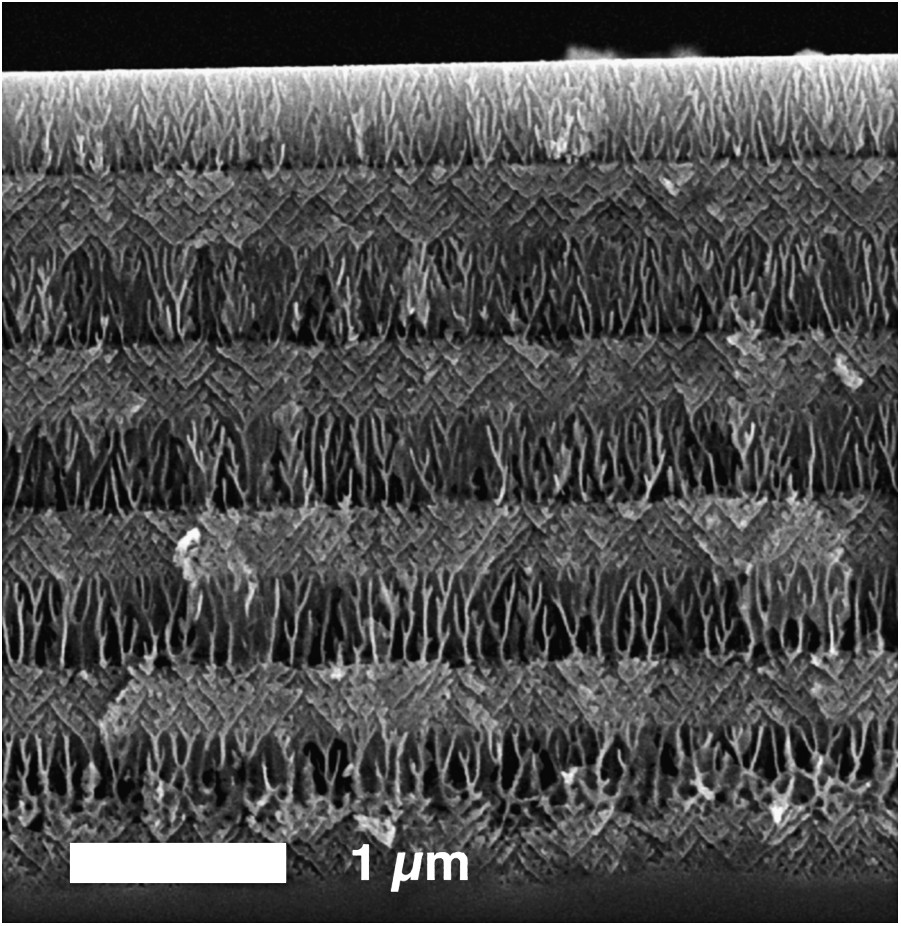
When high currents are applied, porous etching occurs preferentially along the current lines and voltage oscillations correlated to synchronized pore diameter variations are often observed on InP [133], less on GaP [134], GaAs [135] and rarely on Si [136]. This phenomenon has been reported early [18] and diverse groups have investigated it. The influencing parameters have been identified, but a detailed understanding of the oscillating process is still under debate. The oscillation frequency (f) increases with the current density and the temperature [137,138]. The linear increase of f with j indicates that each period contains a constant charge. As seen in Fig. 5 [133], in the case of InP, the voltage oscillations are nicely correlated with synchronized pore diameter variations. In this case, a perpendicular pore branching occurs and is limited by the propagation of the neighbor extensions. Si, InP and more specifically GaAs exhibit also a periodical pore diameter variation that consists of tetrahedral voids [135,139]. The lateral pore expansion is stopped by the dense {111}A facets and further the dissolution proceeds at the tip along the 〈111〉B direction to form a new cavity. In the case of Si, dendritic growth following the 〈100〉 directions occurs [136]. Current oscillations have also been reported [140,141] but pore diameter fluctuations are not often synchronized. It is, however, possible to maintain the simultaneous pore variation established by a galvanostatic treatment in a following potentiostatic polarization [16]. When self-induced voltage oscillations take place, two possibilities are offered. It is possible to suppress it by performing the porous etching at constant voltage and higher temperature [137] or to regulate the frequency and amplitude by applying an additional modulated current with a frequency close to the intrinsic one [142]. It is even possible to apply a modulated current to a system in which self-induced oscillations take place or not in order to get a three-dimensional structured layer [143]. The porous layer exhibits a morphology very similar to the one presented in Fig. 11.
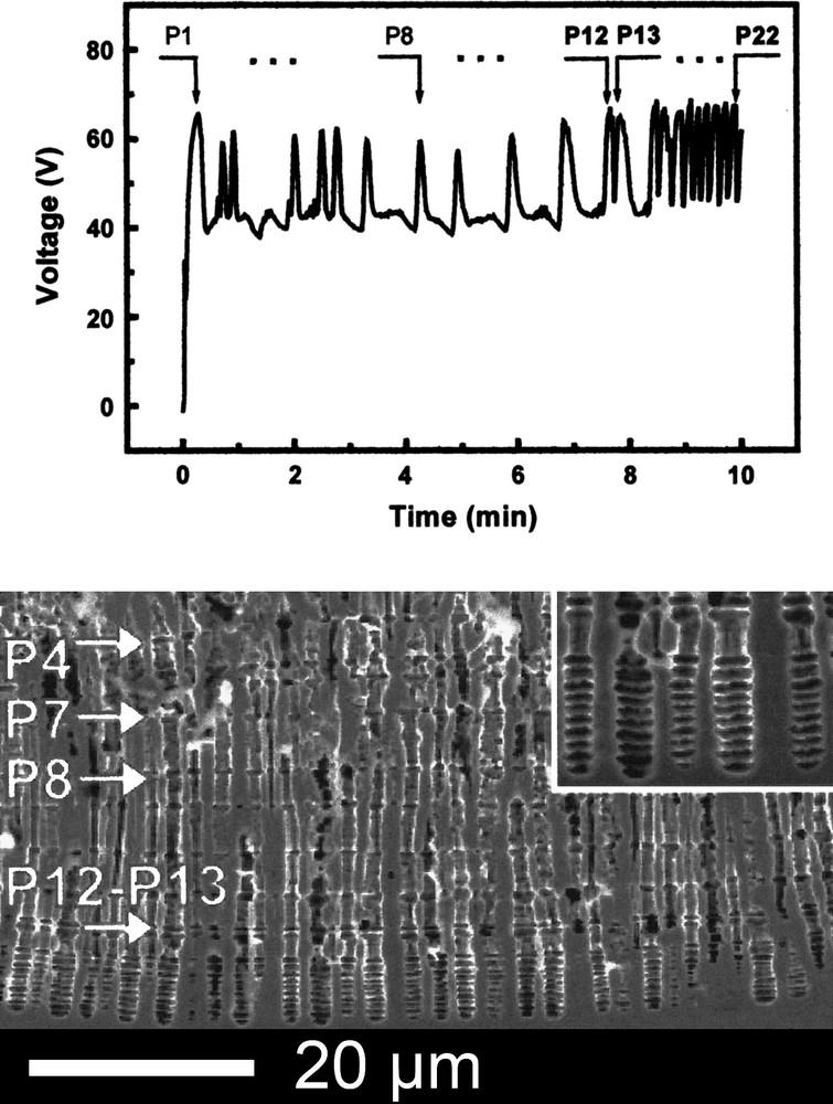
Voltage oscillations (top) and SEM cross-section (bottom) of InP sample anodized at j = 100 mA cm−2 in HCl. The inset is the magnification of the nodes at the bottom of the porous layer (from Ref. [133]).
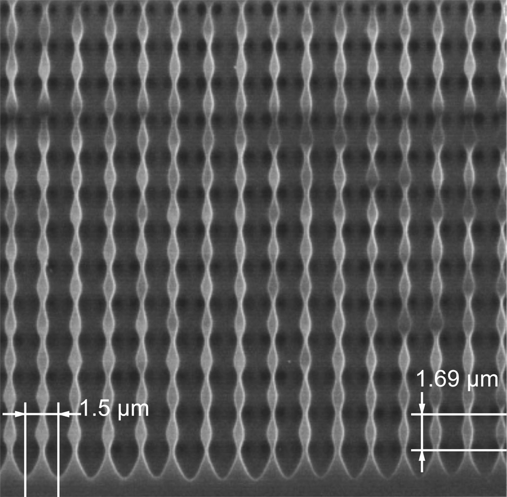
SEM image showing a longitudinal section of the modulated pore structure. The vertical period is 1.69 μm and lateral pore spacing was set to 1.5 μm by lithographic imprints performed by KOH etching (from Ref. [178]).
4.4 Electrolytes
Porous etching of semiconductors has been performed mainly in aqueous media. However, several investigations have been carried out to form pores in non-aqueous electrolytes. According to the literature, it appears that the morphology is strongly dependent on the chemical nature of the solvent, the concentration of the conducting salt, the pH, the counter ion and the temperature.
4.4.1 Aqueous electrolytes
Although silicon etching can be performed in various solutions (see e.g. Ref. [144]) anodic porous silicon can only be grown in hydrofluoric acid containing electrolytes [14]. The etch rate and porosity depend on the electrolyte concentration. Similarly Ge [17], Si1−xGex compounds and all polytypes of SiC can also be made porous using aqueous HF solutions [50,51]. However, square shaped pores and nanowires have recently been grown on Ge in aqueous HCl [145] and NH4F has been successfully used to porosify SiC [146,147].
Due to their different chemical nature, a wide range of electrolytes have been used for III–V compounds. The solutions are chosen to get a pH domain in which anodic films are not chemically stable. Strong acids and bases have thus been mainly used. Pore formation into halogen acids such as HF, HCl, and HBr or in inorganic acids such as H2SO4 and H3PO4 has been reported for GaAs, GaN, GaP and InP (see Table 1 for references). Supplemental reactants have sometimes been added to these electrolytes (e.g. HNO3 or NH4OH + K2PtCl6 in HCl) to improve the pore geometry or to get new morphologies: rectangular or square shaped pores can be formed onto GaP and InP in such specific electrolytes [148–150]. Porous etching of III–V semiconductors in alkaline media is mainly carried out in KOH but successful attempts have been also reported in NH4Cl, NH4Br or NH4OH. Although extreme pH is suitable, it has been demonstrated that pores can be grown in a neutral solution such as NaCl. As seen in Fig. 6, the counter anions X− in halogen acids (with X = F, Br, Cl) play a crucial role determining the pore topography [38]. Note that a porous film exhibiting a different chemical composition than the substrate is formed onto InSb in HX [151] and onto InP in (NH4)2S [152].
Aqueous electrolytes for porous etching of III–V semiconductors
| Semiconductors | Electrolytes | References |
| GaAs | HF, HCl, H2SO4 | [27,31,153] |
| KOH, NH4OH | [29,154] | |
| KOH + KCl | [27] | |
| NaCl | [155] | |
| HF + KI, HCl + KI | [156] | |
| GaP | HF, HBr | [134,149] |
| H2SO4 | [157] | |
| HNO3, HCl, HI, H3PO4 | [158] | |
| KOH, NH4Cl | [156] | |
| H2SO4 + H2O2 | [159] | |
| GaN | H2SO4, H3PO4 | [37,160] |
| Tartaric acid + ethylene glycol + NH4OH | [36] | |
| KOH | [161] | |
| InP | HF, HCl, HBr | [32,38] |
| HCl + H3PO4 | [150] | |
| HCl + HNO3 | [148] | |
| HCl + HNO3 + K2PtCl6 | ||
| HCl + NH4OH + K2PtCl6 | ||
| KOH | [162] |
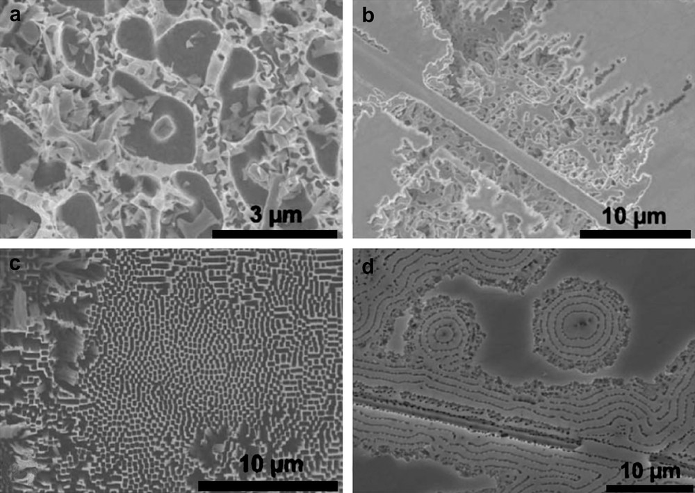
Pore morphologies obtained on GaP with different halide acids after anodization from −2 V to 36 V, scan rate 20 mV s−1 in (a) 0.1 M HF, (b) 0.1 M HCl, (c) 0.1 M HBr and (d) 0.1 M HI (from Ref. [158]).
Semiconductors II–VI have only been porosified in acidic solutions. This can be explained because there are fewer investigations targeting porous etching of these materials than for other semiconductors. A mixture of HCl and HNO3 allows the porous etching of CdSe, CdS while H2SO4 is used for CdTe and Cd1−xZnxTe (see Table 2 for references). H2O2 or K2Cr2O7 is sometimes added for CdTe. Recently Tiginyanu et al. [155] have reported deep pores grown into CdSe in a neutral salt (NaCl) diluted in water (Fig. 4b).
4.4.2 Non-aqueous electrolytes
Organic media have been used to produce new morphologies and to investigate the pore formation mechanisms. Numerous works have used mixtures of aqueous HF with ethanol or methanol because these additions reduce the surface tension and thereby the sticking probability of hydrogen bubbles. Sailor and Doan have for instance fabricated smooth photolithographic porous structures on Si [164] in such ethanol containing electrolytes. Propst and Kohl were the first to report the growth of Si macropores in a “real” non-aqueous electrolyte [110]: hydrofluoric acetonitrile (MeCN). Other organic solvents such as dimethylformamide (DMF) [109] and dimethyl sulfoxide (DMSO) [165] have also been used successfully (see Fig. 7 for examples). Since these electrolytes are all prepared from 48% HF, a small amount of water is always present. In such media almost no hydrogen gas is produced and the oxidation of the substrate is therefore strongly hindered. However, it has been shown that some organic solvents (e.g. DMSO) can act as mild oxidizing agents [166]. Additionally non-aqueous media are very useful tools to investigate the porous etching phenomena in aqueous media since oxygen and hydrogen concentrations can be adjusted by adding either water (O and H supply) or diethyleneglycol (H supply) in the solution. According to Ponomarev and Lévy-Clément [109], the increase of water concentration leads to the favored formation of Si–OH bonds, thus decreasing the overall rate of dissolution allowing the holes to diffuse over the surface, decreasing the pore depth and increasing the pore diameter due to more uniform silicon dissolution. Beside the viscosity and the conductivity of the solvent, it appears, according to the literature, that the pore morphology depends essentially on the polarity, the tendency to oxidize Si, and the H donor properties of the solvent. Pore diameter, depth, roughness or branching can therefore be efficiently tailored according to the electrolyte properties. Similarly to aqueous media, it is thus possible to grow, in organic solvents, meso- and macropores onto both p- and n-Si under illumination or not. Similarly to Si, porous Ge [167] has also been grown in Cl− containing “organic” solutions (AlCl3 or HCl in DMSO or DMF) but water was always present in the solutions.
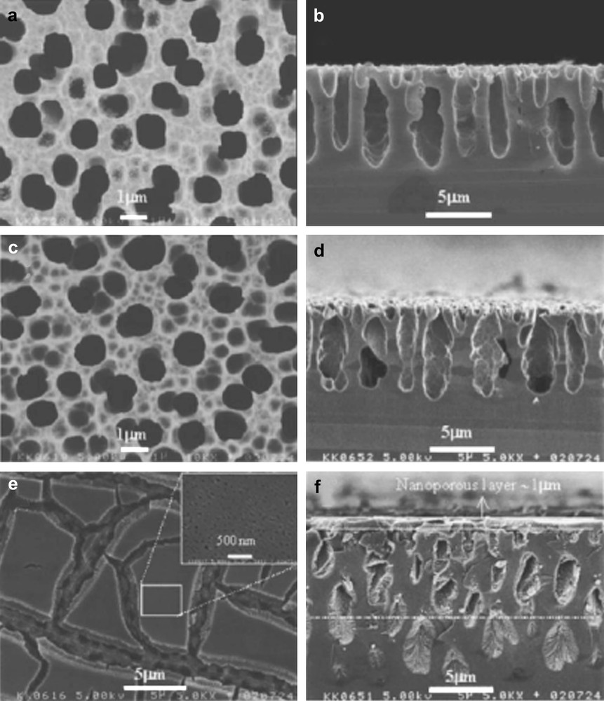
SEM top views (left) and cross-sections (right) of macropores formed by an electrochemical etching of p-Si in 4 M HF containing different organic solvents: (a, b) DMSO, (c, d) DMF and (e, f) MeCN (from Ref. [199]).
Compared to Si, anodic pore formation onto III–V semiconductors has been less investigated in non-aqueous conditions since there is a broad range of aqueous electrolytes (previous paragraph). Porous GaP is obtained in methanol with dilute HF or dissolved Cl gas [33,168]. Ulin and Konnikov have reported electrochemical pore formation onto GaP and InP in NH4Br and NH4Cl containing DMF, respectively [156]. Recently porous layers have been grown onto III–V semiconductors in acidic liquid ammonia at low temperature (−50 °C) [138,169]. In addition to getting new pore morphologies (“coral-like”, Fig. 8), provides true oxygen and water free conditions, i.e. although moisture is present in the solution, the reactivity is ruled exclusively by [170]. These specific conditions have allowed the passivation of the InP surface with a highly stable phosphinimidic amide-like termination (“H2N–PN”) opening therefore new perspectives for the interfacial chemistry onto such substrates. Due to the low viscosity of , porous etching occurs under high mechanical strengths. It induces cracks in the film and multilayered structures.
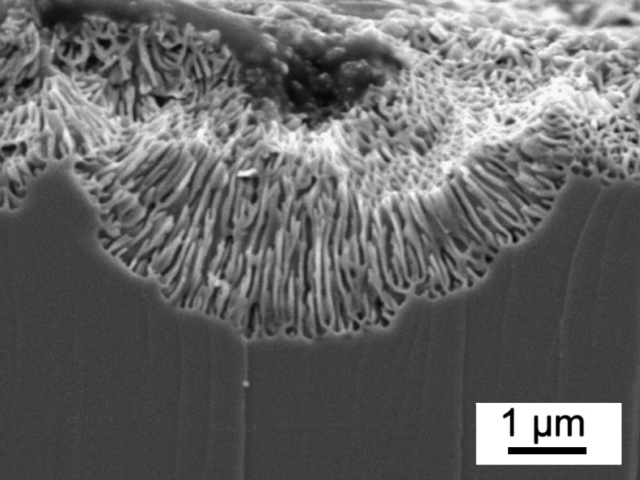
SEM cross-section of porous n-InP grown in 1 M NH4Br/ at T = −50 °C. The porous etching was performed galvanostatically at 2 mA cm−2 for 30 min.
4.5 Pore domains
Depending on the nature of the semiconductor and the electrolyte, porous etching can form domains that result from the branching of a primary pore. The initial pit nucleates at surface defects and propagates in the substrate forming an interconnected crystallographic network. It occurs onto GaP [35], GaAs [171], Ge [172], InP [173], and Si [174]. A competition between uniform and non-uniform nucleation [174] takes place during the dissolution process. The first situation is prevailing when high current or voltage is applied while the second dominates if lower energy is provided. Fig. 9 shows the very specific domain formation onto GaP.
SEM views of n-GaP after anodic etching. The main picture shows the porous domains and the inset presents a cross-section taken along the propagation direction of the secondary pores. The scheme illustrates the five steps of the porous etching: (i) initiation of pores at defect sites, (ii) continued growth of the initial pores, (iii) appearance of the first branches or secondary pores, (iv) further branching, and (v) porous domains meet creating non-porous walls (from Ref. [35]).
4.6 Effect of the doping type and density
Although there is no consensus on the porous etching origins, “physical” and “chemical” approaches are not fully opposing. In practice both concepts have to be considered. The doping density enters in the framework of “physical” models and its effect on the porous etching is indisputable. The doping concentration affects mainly the etch rate, the pore density and the pore wall thickness. As reported in Section 3.2.2, each pore shares with its neighborhood its space charge layer. Hence the pore walls are in full depletion. It is then generally assumed that the pore wall thickness is roughly equal to 2 × WSCL. Since WSCL is inversely proportional to the extrinsic carrier concentration, the doping level will determine the pore wall thickness and the pore spacing (i.e. pore density). Synchronized voltage and pore diameter oscillations are also dependent on the doping concentration: both amplitude and average potential decrease with the doping concentration [133]. Lehmann et al. [175] proposed a detailed listing of the morphological features as a function of doping for p- and n-type Si (see Fig. 10). The tendencies that are proposed can be easily extrapolated for other semiconductors.
Pore spacing is thus controlled by the doping of the substrate. However, pore wall thinning has been recently proposed to modify the layer geometry onto n-InP [176,177]. Cathodic decomposition is indeed possible for n-InP since electrons, necessary for the reaction (see Section 3.1.5), are available on the whole semiconductor surface.
4.7 Illumination
Illumination is used to perform porous etching onto n-type semiconductors. Historically photoelectrochemical porous etching has often been firstly evidenced (see e.g. Ref. [28]). Under adequate lightening electron–hole pairs are created near the surface. Photo-holes move toward the surface and are involved in the dissolution process. Photoelectrochemical etching allows the creation of pores onto low-doped substrates or variation to the morphology since the charge carrier distribution is modified. When the light source is sinusoidally modulated [178], the pore diameter evolves periodically and photonic crystals can be designed as shown in Fig. 11. Backside illumination is also successfully used on n-Si (sometimes on Ge) but it is ineffective for other semiconductors since the minority carrier diffusion length is far smaller than the wafer thickness [104]. As seen in Fig. 1, it allows the formation of perfect tubular pores across the whole wafer thickness.
4.8 Patterning, defect influence and self-ordered structures
4.8.1 Patterning
Pore nucleation can be triggered individually onto silicon surfaces using a lithographic process (see e.g. Ref. [179]). As seen in Figs. 1b and 11, inverted four-sided pyramids are etched in KOH prior to perform the porous etching. If appropriate etching conditions are applied, tubular pores elongate according to the lithographic pre-pattern. Note that the pore spacing has to be adjusted with regard to the doping density since it is the intrinsic parameter. Unsatisfactory attempts have been carried onto III–V compounds [180,181] but these results should not be considered definitive since the porous etching has been performed under CO pores' growth conditions. Carrabba et al. have obtained nice lithographic structures onto GaAs but the photoelectrochemical treatment corresponds to anisotropic electropolishing [182].
4.8.2 Defect influence
Schmuki et al. have proposed a direct patterning method. Pore formation is initiated preferentially at surface defects created in n-Si, n-GaAs and n-InP substrates by Si2+ focused ion beam (FIB) bombardment [87,183,184]. For n-type material in the dark, the electrochemical pore formation potential is significantly lower at the implanted locations than for an unimplanted area. This difference in the threshold voltage is exploited to achieve the selectivity of the pore formation process (Fig. 12). Similar results onto Si and other semiconductors (InP or GaAs) have been reported when mechanical defects are created at the surface by scratching [38,185–187]. In addition to proposed alternative patterning techniques, these works clearly illustrate the crucial effect of surface defects onto the pore nucleation.
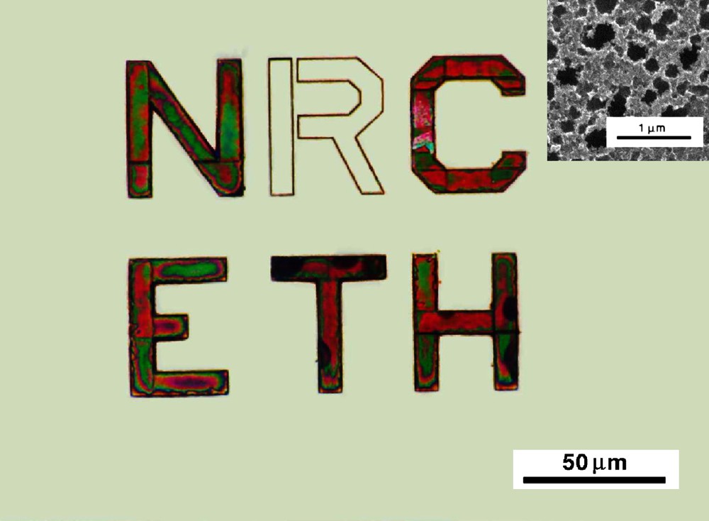
Optical micrograph of porous Si letters produced by Si2+ focused ion beam implantation in n-Si (100) and subsequent electrochemical polarization in HF. The letters show the green and red interference colors typical of PSi. (Inset) SEM image of an implanted zone etched under similar conditions (from Ref. [87]). (For interpretation of the references to colour in this figure legend, the reader is referred to the web version of this article.)
4.8.3 Self-ordered structures
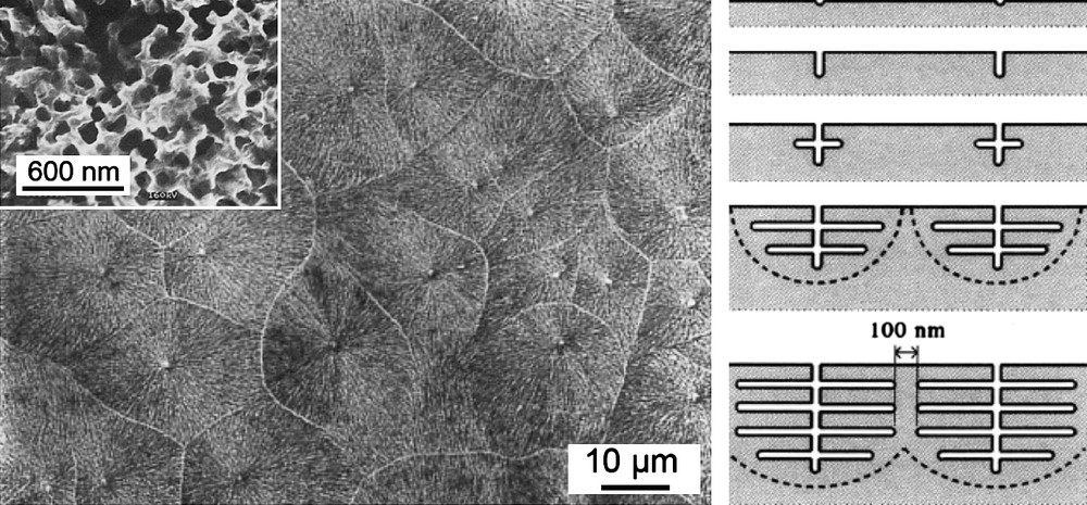
Here it is important to define precisely the denomination. It is obvious that porous layers formed onto a semiconductor are “self-organized” since each pore is influenced by the surrounding pores. However, “self-ordered” structures must exhibit a regular geometry. In 1995, Masuda and Fukuda [60] have reported a nice example of self-ordered anodic porous alumina. Under optimized conditions a highly ordered honeycomb structure was grown onto Al. Self-ordered porous layers have been obtained onto various III–V and IV–IV compounds such as InP [119], GaAs [154], GaP [149] and SiC [188]. As presented in Fig. 13, InP is a good material to illustrate this phenomenon. The authors have shown that the applied potential is the most important parameter to create these ordered structures. When a high voltage is applied, CO pores are formed perpendicular to the surface. This occurs according to a local organization (short-range order) since neighboring pores interact. It is also known that a nucleation layer exhibiting a CO morphology is often formed. This specific crystallographic etching causes the long-range order. The balance between short and long-range ordering is then determined by selecting the right applied potential and temperature.

SEM top views of pore arrays in InP top: (a) nucleation layer of CO pores (b) polycrystal of CLO pores and (c) single crystal of CLO pores. In the case of (b) and (c) the images were taken after removal of the nucleation layers. The insets show the two-dimensional Fourier transforms (from Ref. [119]).
5 Applications
Light-emitting properties of PSi have shown to the scientific and industrial communities the interest of porous semiconductors. Since then the application field has been enlarged to numerous domains: microelectronics, optoelectronics, solar cells, optics, sensors, filtering, micromachining, and medical diagnosis and therapy. Although many investigations have been carried out onto other materials, Si is undeniably preeminent for porous semiconductor applications. In addition to its intrinsic qualities, silicon is nowadays the material for which technology is the most developed and advanced. The specific properties of porous semiconductors result from the intrinsic morphology of the layers (e.g. quantum confinement in microporous Si) or their organizations (e.g. superlattices). In the following a non-exhaustive list points out typical applications of PSi in different fields: isolation technique in silicon integrated circuits based on IPOS (insulation by oxidized porous silicon) [20], visible light-emitting devices integrated into microelectronic circuits [189], anti-reflecting system in solar cells [190], bioactive devices [22], cathode in rechargeable Li-ion batteries [191], explosive materials and its use in atomic emission spectroscopy [25], and membranes to separate macromolecules [192]. Si superlattices are used as waveguides [126], microcavities [193,194], Bragg reflectors [122,125], and interferometric biosensors [195].
Acknowledgements
The authors would like to acknowledge Alexandra Eb (University of Versailles) for her help in finding old references and Dr. Michael. J. Graham (National Research Council of Canada) for his careful reading.
1 International Union of Pure and Applied Chemistry.