

1 Introduction
Nowadays, due to the miniaturization revolution, there is a growing need for methods that produce thin inorganic or hybrid organic–inorganic films on conducting 2D patterns and 3D geometries. Coating of conducting parts with complex shapes with oxide films is a non-trivial task, which requires sophisticated tools [1]. For instance, printed chips are traditionally coated by the use of chemical masks [2]. By this process, the chip is coated by an appropriate mask, followed by etching or wet deposition of the oxide thin film. However this coating procedure is time consuming, the etching chemicals are usually quite hazardous, the resolution of the coating is usually insufficient, and often the etching creeps beyond and below the predetermined boundaries. Furthermore, this method is incompatible for the coating of 3D samples, such as metal grids and porous objects. It should be noted that electrophoretic methods have been used for coating of complex geometries such as porous carbon electrodes [3,4]. However, the high roughness of the products—as well as the common use of micrometric-size particles—are not suitable for the submicrometric details found on most printed chips [5,6]. Electrophoresis has another fundamental disadvantage, namely the high voltages that are usually applied, which may damage the sample to be coated. Hence, a new coating method that can distinguish between the conducting and insulating areas of a complex geometry is desired.
We have recently developed [7–11] a convenient low-voltage electrochemical method that is based on the sol–gel process for the fabrication of silica (SiO2), zirconia (ZrO2) and titania (TiO2) thin films, their organic derivatives, such as methylated-silica (CH3SiO3/2) and their doped versions, such as organically doped titania [10] and silica or titania doped with metallic copper [11]. These films exhibit extremely low roughness, and their thickness is easily controlled by altering either the applied potential or its duration.
Here we show that this general methodology is suitable for solving a classical problem in thin-films technology: dip-coating, spin-coating, spraying without masks—all cannot be used for selective coating of a complex conductive pattern, because these methods do not differentiate between conducting and non-conducting areas. We show that our low-voltage electrochemical methodology solves this problem, by demonstrating its action where it is needed most, namely in printed circuits (sputtered aluminum patterned chip), studying first as a model a gold mesh; in a sense, we provide here a method for “electrochemical pattern recognition”.
2 Experimental details
2.1 Chemicals and materials
Lithium perchlorate (LiClO4) and titanium tetra-n-propoxide (98%, Ti(OPr)4) were from Aldrich. Zirconium tetra-n-propoxide (70% Zr(OPr)4 in n-propanol) was from ABCR. 2-propanol (2-PrOH) was from J.T. Baker and was dried over molecular sieve 0.3 nm (Fluka) for at least 1 week before used. TDW (EasyPure, Barnstead) was used in all the experiments. Gold meshes were acquired from Good Fellow Co. (PA, USA). The sputtered aluminum circuit was received from Intel Co.
2.2 Deposition solutions
The titania deposition solution was prepared by adding 16.15 mL of dry 2-PrOH that was wetted with 160 ppm water and 0.1 M LiClO4 to 0.95 mL Ti(OPr)4 under vigorous stirring (monomer concentration was ca. 0.2 M). The Zr-deposition solution was prepared by adding 5 mL of dry 2-PrOH that was wetted with 900 ppm water and 0.1 M LiClO4 to 5 mL Zr(OPr)4 under vigorous stirring (monomer concentration was ca. 1.12 M).
2.3 Film deposition
During the electrochemical deposition, a potential of −1.4 V vs Ag/AgBr was applied for duration of 15 min (in the Ti-system) or 30 min (in the Zr-system), while stirring the solution. Comparative dip-coating was performed by pulling the substrate at a rate of 50 μm sec-1 from the deposition solution while stirring. Films were characterized by Sirion (FEI) high-resolution scanning electron microscope (HR-SEM), which provided also the elemental EDS data.
3 Results and discussion
3.1 Electrodeposition on a gold mesh
The gold mesh (mesh 1500) has a repeating square unit every 16.9 μm and the thickness of the gold wire is of 6.5 μm (Fig. 1a). The open area of these meshes is quite large: ca. 88% of the total area. Coating of the mesh with titania film was carried out by either dip-coating (Fig. 1b) or electrodeposition (Fig. 1c). It is evident from these images that electrodeposition generates thicker coating in comparison to dip-coating. Indeed, from independent thickness measurements, the thickness of the former (upon applying −1.4 V for 15 min) was ca. 500 nm, whereas the thickness of the latter was only ca. 10 nm. A detailed explanation for this was provided in our earlier publications [9] (see also Mechanism, below). In brief, upon applying potentials, the solvent is reduced at the electrode, leading to an increase of pH levels at the electrode surface. This pH change accelerates the polycondensation of the monomer at the electrode, leading to the deposition of thicker films.
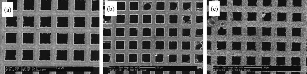
HR-SEM images of: a: bare gold mesh; b: gold mesh coated by TiO2 upon dip-coating; c: gold mesh coated by TiO2 upon applying –1.4 V for 15 min. The bar is 20 μm.
The distinction between the two procedures for coating is also evident in EDS-element mapping (Fig. 2). The bare mesh does not contain Ti (Fig. 2a). However, upon electrodeposition this element clearly appears to coat the mesh (Fig. 2b,c). As is seen, dip-coating results in the thinner film (Fig. 2d).
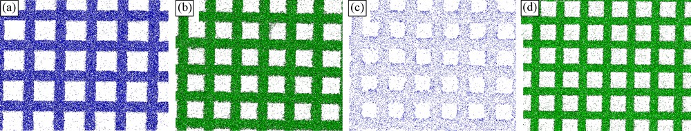
EDS element-mapping of: a: bare gold mesh (seen is Au); b: gold mesh on which TiO2 was electrodeposited upon applying –1.4 V for 15 min (seen is Ti); c: the residual underlying gold in b; d: gold mesh coated with TiO2 upon dip-coating (seen is Ti).
3.2 Electrodeposition on an Al-sputtered circuit on Si
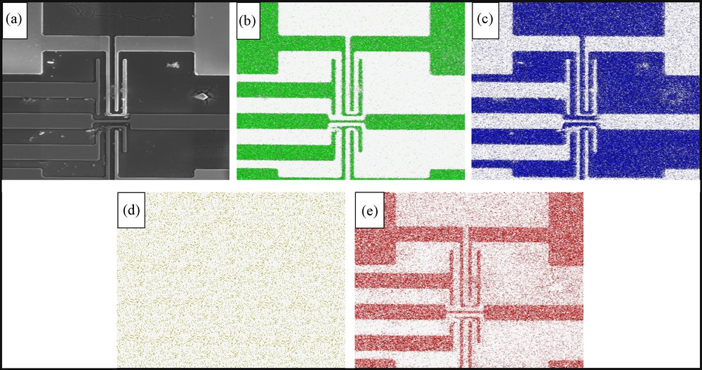
Whereas in the previous model example, coating of unwanted regions has not been a requirement, in printed circuits one wishes to deposit an overlayer only on the pattern or on its negative. Standard film coating can be applied only if wetability or adhesiveness of the different zones is completely different on the printed zone compared to the support area; this is usually not the case. Our second and third examples are the electrodeposition of either ZrO2 or TiO2 thin films on an Al conductive micron-scale pattern, which was sputtered on a Si wafer (Fig. 3a-c). A major achievement has been the exact coating of the patterned circuit only. Whereas dip-coating in the zirconia deposition mixture causes the pattern to totally disappear (Fig. 3d), clean deposition of ZrO2 film on the Al pattern is seen on Fig. 3e. AFM pictures of the zirconia film are provided on Fig. 4 (on ITO, for further comparison purposes), and it is seen that the electrodeposited film is much smoother than the dip-coated one. Finally, the generality of the approach is seen on Fig. 5, where this time the cleanly deposited film is TiO2.
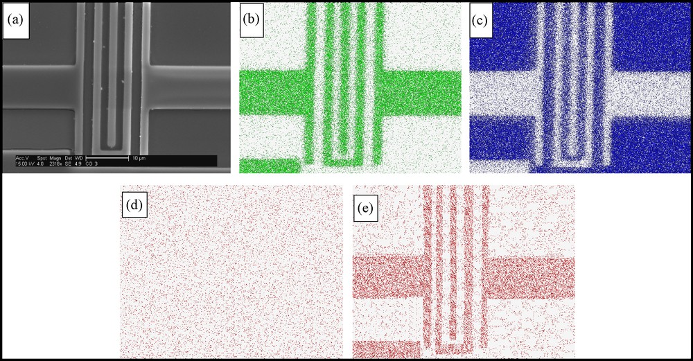
Pattern-selective electrodeposition of ZrO2. a: HR-SEM image of a sputtered conductive circuit of Al on Si (the bar is 10 μm); b–c: EDS element-mapping of the sample. Seen are Al and Si, respectively; d: the sample after dip-coating with ZrO2 precursors (seen is Zr; it coats the entire surface); e: EDS element-mapping of the sample coated by ZrO2 upon applying –1.2 V for 30 min (seen is Zr).
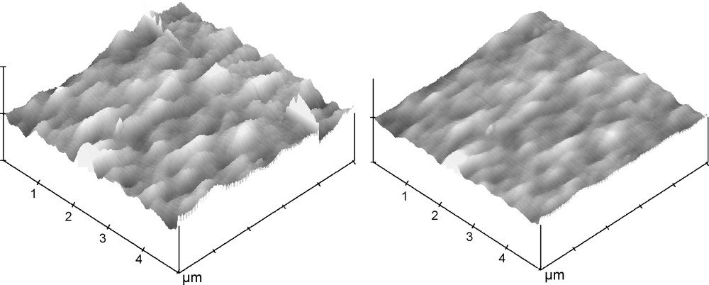
AFM images of zirconia, left, dip-coated, and, right, electrodeposited (–0.9 V for 30 min, on ITO; x, y-scales: 5 μm × 5 μm; z-scale: 20 nm).
Pattern-selective electrodeposition of TiO2. a: HR-SEM image of the same sputtered conductive circuit of Al on Si (shown is a different section of it); b–c: EDS element-mapping of the sample. Seen are Al and Si, respectively); d: the sample after dip-coating with TiO2 precursors (seen is Ti; it coats the entire surface); e: EDS element-mapping of the sample coated by TiO2 upon applying −1.4 V for 15 min (seen is Ti).
3.3 Mechanism
We comment now on the mechanism of the pH jump, which is the key for the electrochemical trigger of the sol–gel process; we use the zirconia case as a model [9]—for titania, the considerations are similar [10,11]. Since Zr(OPr)4 is not electroactive through the applied potential window, one has to take into account the electroactivity of both the solvent and the added water. The reduction of 2-propanol is likely to give the alkoxide ion [12] and therefore, the two reduction processes are the following:
The alkoxide, which is electrochemically formed, reacts with water to yield hydroxyl ions as well:
| (CH3)2CHO− +H2O → (CH3)2CHOH + OH− |
The anodic processes result in increase of the local concentration of protons by either generating ketone [12] or oxygen:
| (CH3)2CHOH → (CH3)2CO + 2H+ + 2e− |
4 Conclusion
In conclusion, we have shown in this paper the feasibility of pattern-selective electrodeposition of oxide on the conducting parts of complex geometries. The samples that were used in this study were Al-sputtered circuits and a gold grid. We demonstrated that dip-coating from the monomer solution results in homogenous films that were deposited on both the conducting and insulating areas of the sputtered circuits. However, upon applying negative potentials, the conducting areas were selectively coated by either ZrO2 or TiO2 films. Many applications of this useful methodology can be envisaged.
Acknowledgements
The Ministry of Science and Technology of Israel is acknowledged for supporting this project under the Tashtiot Project.