

1 Introduction
Due to their appealing properties, one-dimensional (1D) nanostructures, including rods, belts, pillars, wires and tubes have attracted attention in the field of nanotechnology [1–4]. Elaborated from different materials like metals, semiconductors, insulators, organic and bioactive species, these low-dimensional objects are characterized by transportation of charge carriers in one dimension, making them highly powerful when a strong anisotropy is required [5]. For instance, in photovoltaics, such a configuration is very interesting because the electron–hole recombination in one plane can be limited, enhancing drastically the photoconversion efficiency. Even more convincing is the strong impact of wire-shaped 1D nanosystems in microelectronics for their ability to be used as chip interconnections and as elemental building blocks in functional devices. Particularly, the remarkable magnetic properties of Ni-, Fe-, and Co-based nanowires have opened new perspectives to fabricate the next generation of recording nanodevices with a high capacity of information storage [6].
Today, the fabrication of wires in the sub-micrometer range can be achieved through two strategies, so-called bottom–up and top–down. In the first approach, both self-assembly and self-organization processes are utilized to produce different templates dedicated to the synthesis of nanowires. The templates can be elaborated from e.g. self-assembling of molecules (organic and biological), reconstruction of surfaces, misfit dislocations, stress-assisted cracks, etc. [7–12]. Regarding technical and economical aspects, the bottom–up approach is very attractive, but most of the time arrangement and organization of the templates are not accurately controlled. Thus, this strategy has to be generally coupled with other techniques.
The top–down approach covers multiple lithographic techniques that have been mainly developed for applications in semiconductor industry. In general, the lithographic sequence begins with the localized chemical modification of a positive resist (polymer layer) using either a direct (maskless) or a non-direct exposure system (Fig. 1a). As irradiation of the resist leads to the breakage of the polymer chains, positive resists become more soluble in solvent after exposure and the exposed regions containing material of lower mean molecular weight can be selectively dissolved after development (Fig. 1b). Finally, the channels that are opened in the polymer layer can be filled with materials (Fig. 1c) before removal of the unexposed resist, leaving the nanowires onto the surface (Fig. 1d). It is worthy to note that the direct and complete filling of channels is mainly achieved by a bottom–up technique. Indeed, top–down techniques like chemical vapor deposition (CVD), physical vapor deposition (PVD), or electron-beam evaporation (EBE) lead to gradual accumulation of materials at the top of the resist, closing the openings of the structures during evaporation. Thus, a bottom–up approach like electroplating is a convenient electrochemical tool to fill resist-free parts while ensuring an excellent lateral resolution. For example, planar nanowires with line width smaller than 50 nm have been obtained by combining electron-beam lithography (EBL) and electrodeposition process (Fig. 2a).
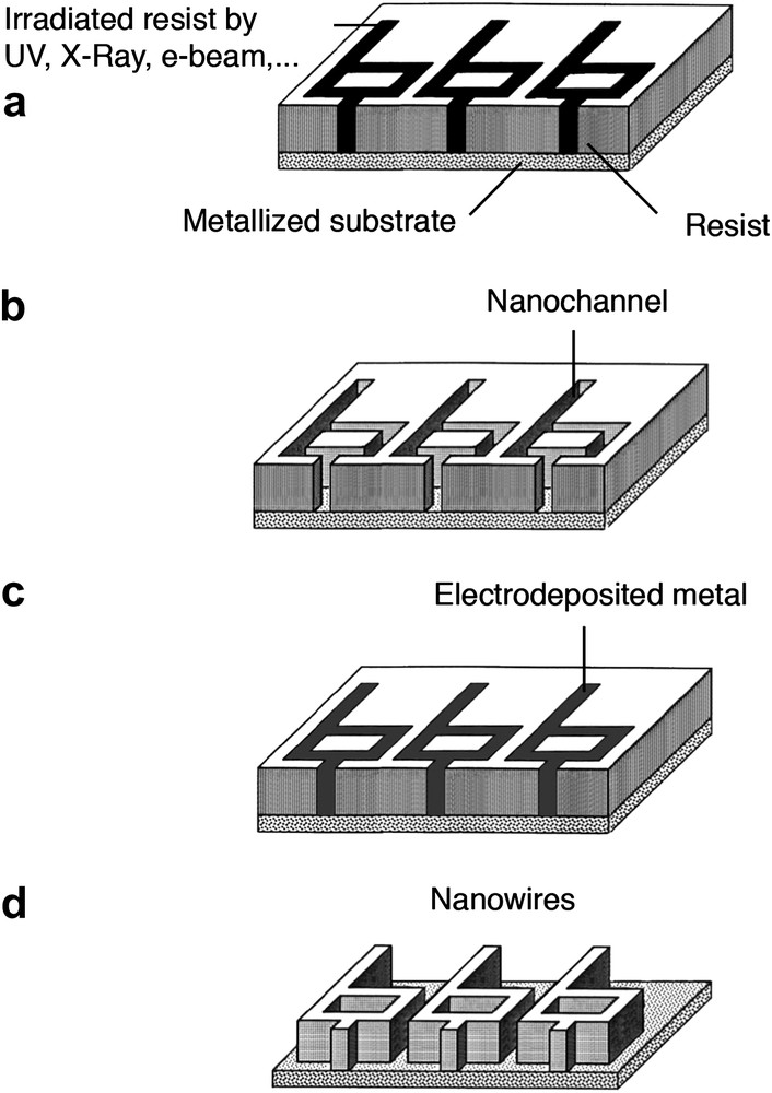
Description of nanowire fabrication using a conventional lithographic sequence with EDP. (a) Exposure of resist; (b) development of exposed resist; (c) electrochemical deposition; (d) removal of resist.

Horizontal metallic nanowires fabricated by EBL and electrodeposition process (a); 3D microwires obtained by LIGA process (b). Courtesy of the Synchrotron Radiation Source at Daresbury, UK.
2 Background
With the development of microelectronics and the systematic needs for shrinking the dimensions of the nanostructures, multiple alternative top–down approaches combined with electrochemical techniques have been explored—e.g. particle-beam or scanning probe lithographic techniques [13–19]. However, a large majority of these strategies are limited to the planar technology and suffer from disadvantages, like optical diffraction, low speed-writing, weak throughput, and high cost. At the moment, X-ray lithography is the most powerful technique employed for the fabrication of non-planar nanostructures, because the optical diffraction limitations are considerably reduced, resist film is transparent to X-rays (high-aspect ratio pattern fabrication), and undesired scattering and reflection are negligible. Thus, the LIGA process—a German acronym for Lithographie, Galvanoformung, und Abformung (lithography, electroforming, and molding)—combining X-ray lithography with electroplating remains the best top–down strategy used for the formation of 3D features revealing a high-aspect ratio. An example of Ni microwires obtained by the LIGA process is given in Fig. 2b. Although LIGA is exploited for the fabrication of micro-electromechanical systems (MEMs), it has been held back from large-scale manufacturing by a variety of technical and economical limitations. In this context, the growth of nanowires has been investigated by alternative techniques including e.g. chemical vapor deposition (CVD) processes, laser ablation, membrane-assisted deposition or catalytic growth via the so-called vapor–liquid–solid (VLS) mechanism [20–22]. Particularly, the synthesis of nanowires based on semiconducting materials such as Si or ZnO has been widely studied by wet and dry processes. For more details, see e.g. Refs. [23–28]. However, the exploration of alternative tracks allowing the control of both the size and the shape of the nanostructures is still needed. Among all techniques recently reported, those based on an electrochemical deposition process (EDP) are strongly emerging, because of significant technical and economical advantages, such as simplicity, low cost, and even more important, the ability to operate at low temperature and in different media. Therefore, EDP is one solution of choice for the formation of 3D structures with tailored dimensions—see for instance a report about the synthesis of ZnO nanowire arrays [29]. Particularly, the fabrication of vertical nanowires that are composed of tin (metal, oxides, and alloys) presents a large spectrum of promising applications in microelectronics, sensing [30], and solar cells [31]. Hence, these high-aspect ratio 1D nanostructures based on tin and tin oxides have also been exploited for the conception of new nanometer-scale devices including nano-FETs (field effect transistors), nano-LEDs (light emitting diodes) as well as the design of 3D microbatteries for instance with the conception of nano-architectured anodes for rechargeable lithium batteries [32].
In this paper, the main recent techniques employed for the electrochemical growth of tin nanowires are shortly reviewed. After a brief overview of the strategies that have been studied in the last decades, a novel protocol based on the formation of tin nanowires which are electrochemically grown on titania nanotube guide layers will be presented.
3 Membrane-assisted nanowire fabrication
A versatile route for preparing tin nanowires involves electrodeposition of crystallites into a porous template, which is subsequently dissolved as it is described in Fig. 3. This template-assisted electrochemical synthesis provides a convenient and reproducible method for the preparation of uniform nanowires of various lengths and diameters. At the moment, the most encountered templates consist of two sorts of nanoporous membranes that are rapidly described in the next sections.
Schematic representation of the template-assisted electrochemical synthesis method. Ion irradiation of a polymer foil (a); chemical etching of the ion tracks (b); deposition of a conductive layer and filling of the pores (c); dissolution of the membrane (d).
3.1 Polymeric track-etched membranes
This type of membranes is obtained by the irradiation of a polycarbonate foil with heavy ions, e.g. Au, having specific energies higher than 1 MeV/nucleon (Fig. 3a). Ion bombardment is performed through a circular metal mask with an aperture diameter of 0.2 mm. The fluences used for irradiation are typically in the range from 1 ion/sample to 107 ions cm2. Then, selective etching is carried out in alkaline solutions after exposure to UV for a better track-etch sensitivity (Fig. 3b). As the etching rate of exposed and non-exposed regions is drastically different, the final morphology of the nanochannels will be strongly dependent on the etching conditions (chemical composition of the bath and temperature). In 5 M NaOH and 10% vol methanol at 50 °C, cylindrical pores are obtained for high track-etch rate to bulk-etch rate ratios, while in 9 M NaOH and 10% vol methanol at room temperature low ratios lead to conical-shaped pores. Cylindrical or conical-shaped nanowires are obtained after electrochemical filling of the nanochannels formed in the polycarbonate foil (Fig. 3c), followed by the selective dissolution of the host membrane in an adequate solvent (Fig. 3d). For the case of tin nanowire fabrication, it has been reported that the electrochemical deposition of Sn crystallites by potentiostatic experiment was performed in a 41.8 g/l Sn(BF4)2 electrolyte using a homemade track-etched polycarbonate membrane (50 μm in thickness with pore diameter ∼55 nm and pore density ∼2 × 109 cm−2) [33]. It can be noted that this approach based on the use of a polymeric track-etched membrane combined with EDP processes has also been sucessfully used to fabricate different metallic nanowires, including Cu, Au, Pb, Ni, Cu-based alloys, etc. (see e.g. Refs. [34–37]).
3.2 Anodic alumina membrane
The use of nanoporous anodic alumina membrane (AAM) as a template is currently the most attractive technology to grow Sn-based nanowires. Highly ordered AAMs are simply fabricated by anodization of aluminum foils, either in H3PO4, (COOH)2 or in H2SO4 electrolytes [38,39]. Fig. 4a and b shows the SEM images of a honey-comb AAM with a high-aspect ratio (around 400) obtained by a three-step procedure (i) anodization at 40 V during 2 h in 0.3 M C2O4H2·2H2O, (ii) heating treatment performed at 60 °C in 0.6 M H3PO4 + 0.2 M CrO3 during 30 min, and (iii) anodization at 40 V during 3 h in 0.3 M C2O4H2·2H2O. The diameter of this two-dimensional array of nanoholes—in the range of 40–90 nm—can be adjusted by the pore widening treatment in 5 wt% phosphoric acid during 30 min at 30 °C. It has to be noted that the fabrication of AAM can also be performed by other techniques. Indeed, the formation of monocrystalline pore arrays in anodic alumina has also been achieved by EBL [40]. For this, the hexagonal pattern is written on the PMMA resist hole by hole with EBL. After removal of the irradiated parts, the pattern is transferred onto the Al substrate by using a wet chemical etch in phosphoric and nitric acids. Then, PMMA is removed and the Al substrate is finally anodized in an oxalic acid solution under constant voltage. When the pore distance, which depends on the anodic voltage, matches the prepattern pitches well, the pattern can act as initiation points and guide the pore growth in the anodic film. Fig. 4c shows an SEM micrograph of an ordered pore array prepared with 200 nm interpore distance. In this case, the anodic voltage was adjusted to 85 V based on the relationship between the pore distance and the anodic voltage. Under these conditions, very high-aspect ratio (around 500) has been obtained.

SEM images of nanoporous alumina obtained by electrochemical anodization (a, b) and by EBL combined with etching (c). From Ref. [40].
The sequence used to grow tin nanowires from AAM is outlined in Fig. 5. In practice, the hexagonal closely packed porous alumina template is obtained from the bulk material by (i) removing the Al layer in a saturated HgCl2 solution and by (ii) removing the barrier layer on the bottom side of the AAM by etching treatment performed in a phosphoric acid solution at 32 °C for 60 min. Then, a metallic layer, in general an Au thin film, is sputtered on one side of the membrane. This conductive layer serves as a working electrode in a standard three-electrode electrochemical cell. Before EDP experiment, the AAM has to be immersed in deionized water under ultrasonic agitation for 2 min for cleaning and for expelling air bubbles from the pores. This procedure is suitable to grow uniform and continuous nanowires. Electrodeposition of Sn within AAM has been demonstrated by galvanostatic experiment, i.e. by applying a constant direct current density of 0.75 mA cm2 for 1 h in a solution containing tin dichloride of 7 g l−1 and sodium tricitrate of 25 g l−1. Then, Sn nanowires have been obtained after removal of the AAM by a wet etching carried out in 0.5 M NaOH.
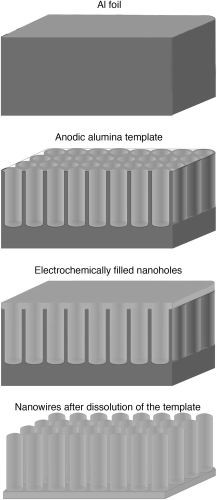
Schematic representation of the electrochemical fabrication of Sn nanowires using AAM template.
It can be noted that this procedure has been initially established to produce SnO2 nanowires. For this, Sn embedded in AAM can be either anodized at 10 V in 0.2 M boric acid or simply annealed in air at 923 K for 10 h. This latter treatment leads to the formation of pure SnO2 without the presence of SnO [41,42].
4 Electrochemical growth of Sn nanowires on titania nanotube guide layer
It is remarkable that both patterning and templating methods mentioned so far require the removal of the resist or the membrane, respectively. Furthermore, the length, diameter, and density of Sn nanowires are directly dependent on the properties of these layers. Recently, we have described a novel route for the formation of tin nanowires which are electrochemically grown on nanostructured titania layers. We have reported for the first time that self-organized TiO2 nanotubes can guide the growth of tin nanowires by using a two-step electrochemical process: (i) formation of self-organized titania nanotubes by anodization of a sputtered Ti thin film and (ii) electrochemical growth of Sn nanocrystallites directly on the tubular TiO2 layer [43]. The principle of this method is depicted in Fig. 6. Compared to the conventional techniques employed for the fabrication of nanowires, this alternative template approach shows two main differences: subsequent dissolution of the titania template after deposition of Sn is not needed and structural properties of the Sn nanowires can be monitored by EDP parameters, i.e. current density and deposition time.

Schematic representation of the electrochemical fabrication of Sn nanowires using self-organized titania nanotubes.
In practice, the sequence starts with the deposition of a 2-μm-thick Ti film onto a Si wafer by cathodic sputtering using a DC triode system. Then, sputtered Ti thin film showing a columnar morphology (see Fig. 7a) is anodized in a fluoride-containing electrolyte in order to form self-organized TiO2 nanotubes. The potentiostatic treatment performed at 20 V during 20 min in 1 M H3PO4, 1 M NaOH and 0.5 wt% HF leads to the formation of TiO2 nanotubes characterized by an average length of approximately 600 nm, a diameter between 80 and 150 nm, and a wall thickness of 20 nm. Fig. 7b and c shows the SEM top view of nanostructured titania template and the corresponding cross-sectional view obtained after anodization. It can be noted that the fabrication of functionally self-organized TiO2 nanotubes has been the subject of multiple investigations [44–46], since Kelly has reported for the first time the ability to produce nanostructured titania by anodization of Ti foil in fluoride-containing medium [47]. Such a discovery has precipitated the publication of many reports [46,48–50], including recent works that have demonstrated that self-organized TiO2 can also be elaborated by anodization of sputtered Ti thin films on different substrates like glass [51], silica [52], and p-type Si(100) at room temperature [53].
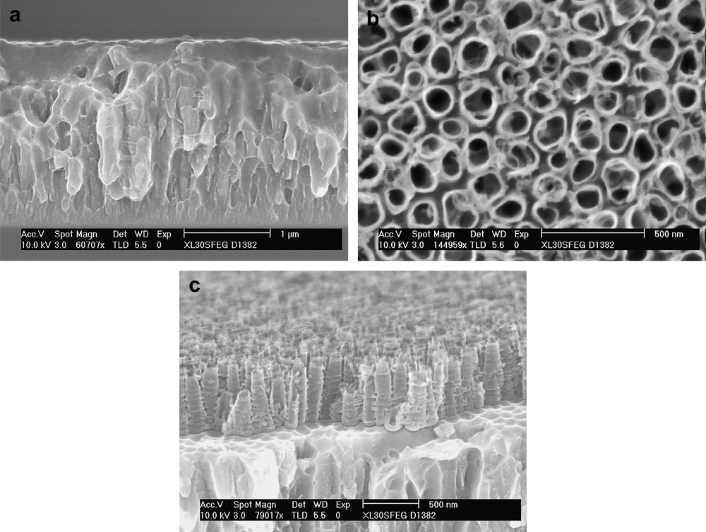
SEM images of columnar Ti thin film sputtered on p-type Si(100) before anodization (a) and after anodization at 20 V for 20 min (b and c) in an HF-containing electrolyte.
The second step of the procedure consists of growing Sn crystallites directly on the nanotubular titania layer by galvanostatic experiments carried out in Sn2+-containing electrolyte. According to Fig. 8 showing the SEM image and the size distribution of Sn crystallites, it is clearly apparent that the large majority of the deposit consists of nanowires that can be up to 2.5 μm long with a diameter below 300 nm when a constant current density of −2.5 mA cm−2 is applied for 3 min in 0.036 M SnCl2 + 0.05 M Na3C6H5O7·2H2O. Our recent work has shown that the electrochemical deposition of Sn performed on a flat compact titania layer leads solely to the growth of huge crystallites confirming that the nanotubular morphology is responsible for the formation of vertical dendrites. The mechanism of dendrites formation under different electrochemical conditions has been the subject of intense investigations [54–56] and the formation of Sn crystallites revealing a whisker-like structure can also be found in literature—see e.g. Refs. [57,58]. However, most of the efforts contributed to suppress this undesired morphology in order to produce homogeneous Sn thin films [59–62]. For the moment, the preferred orientation growth of Sn crystallites encountered in this work could be attributed to a “tip-effect” leading to a very high current density at the top part of the Sn nuclei. This localized current density could enhance drastically the growth of dendritic crystallites, resulting in the formation of wires. Although the formation of nanowires remains unclear, the SEM image presented in Fig. 8 shows clearly that the presence of nanotubes can be exploited to initiate and guide the electrochemical growth of vertical Sn wires in the sub-micrometer range. Furthermore, it is also remarkable that the width of several wires fits quite well with the nanotube aperture (between 80 and 150 nm), emphasizing that dimensions of the nanowires can be comparable to the diameter of the nanotubes. This first work has also shown that the properties of Sn nanowires in terms of structure and density can be controlled by EDP parameters. For instance, decreasing the applied current density can limit the contribution of the coalescence phenomenon, leading to the formation of nanowires with a homogeneous size distribution. This work has also suggested that the diameter of the nanowires could be controlled by tailoring the diameter of the nanotubes and EDP parameters thereby opening interesting perspectives towards the fabrication of self-organized Sn nanowires.

SEM tilted view of Sn nanowires prepared in 0.036 M SnCl2 + 0.05 M Na3C6H5O7·2H2O by applying a current density of −2.5 mA cm−2 for 3 min (a); distribution of Sn crystallite diameters (b). From Ref. [43].
5 Conclusion
In this work, the fabrication of Sn nanowires using different electrochemical methods is briefly reviewed. Firstly, it is reported how template-assisted technologies can be used to produce 3D nanostructures. Compared to conventional patterning techniques, the high degree of reproducibility combined with the economical considerations makes template-based approaches the most attractive way. For the moment, the use of membranes as templates associated with electrodeposition of Sn is the most convenient route to achieve the fabrication of nanowires with controlled dimensions and density. However, alternative techniques are currently investigated in order to simplify the procedure and control the properties of Sn nanowires by monitoring only EDP parameters. Particularly, the ability to grow Sn nanowires on self-organized titania nanotubes without dissolution sequence is reported here. This last approach has demonstrated the ability to grow Sn nanowires by simply controlling EDP parameters and is promising for the fabrication of a wide range of nanowires aiming at many different applications.
Acknowledgments
We thank the “Agence nationale de la recherche” (“LIBAN” project) for financial support, and A. Tonetto and R. Notonier for SEM images (“Centre commun de microscopie électronique”, Saint-Charles).