

1 Introduction
A great deal of interest in localized dissolution and formation of porous semiconductors was triggered by the observation of efficient luminescence from porous silicon [1]. Recently, an increasing number of papers has been devoted to the preparation of porous III-V semiconductors [2–4] and their potential applications [5]. On the other hand, applications of porous substrates in heteroepitaxial growth are rare and investigations in this field are far from being systematic [6–8].
Epitaxial growth has always been a marriage of convenience between deposited layer and substrate. In the simplest case, both the layer and substrate are of the same material, providing a perfect homoepitaxial match. However, due to the existence of a limited number of substrates, which are available at acceptable quality and cost, restriction to homoepitaxial systems would greatly limit the number of applications. This limitation was the main driving force behind the progress of semiconductor epitaxial growth towards pseudomorphic, lattice mismatched heteroepitaxial systems, where small amount of strain is accommodated in very thin layers and multilayers. It was the development of vapor phase epitaxial techniques (molecular beam epitaxy and metalorganic vapor phase epitaxy) that allowed for the deposition of these systems with precise control and uniformity. Still, when the critical layer thickness is exceeded, misfit dislocations are created [9]. Dislocations greatly affect performance, reliability and lifetime of semiconductor devices [10,11]. A number of defect engineering approaches have emerged to gain control over the generation of defects during heteroepitaxial growth. Some of them intend to remove existing defects from lattice-relaxed layers (graded or superlattice buffer layers [12], epitaxial lateral overgrowth [13]), others try to avoid lattice relaxation by using reduced area growth and patterning [14,15], compliant substrates [16], or nanoheteroepitaxy [17,18].
A long time ago, it was proposed that porous substrates should be able to accommodate elastic strains generated at the heteroepitaxial interface of lattice mismatched materials during its formation and subsequent cooling [19]. We have recently demonstrated that a microlamellar porous structure may be suitable for the lattice mismatch compensation in the lattice mismatched epitaxial growth from the liquid phase [20]. An essential step in successful application of porous substrates in epitaxial growth is to achieve control over their properties: the pore size, orientation, density and depth.
We report on the growth of InxGa 1-xAs epitaxial layers by metalorganic vapor phase epitaxy on porous GaAs substrates prepared by anodic etching. The indium content is varied and so is the misfit between the substrate and the epitaxial layer. The surface morphology and photoluminescence efficiency of the layers is investigated and a comparison between the layers grown on conventional and porous substrates is given.
2 Experimental
The pore etching was carried out in an electrochemical cell containing a fluoride-iodide aqueous electrolyte (H2O-HF-KI) using a three-electrode configuration. A home-made potentiostat/galvanostat was computer-controlled and allowed to monitor all process variables. Vetical gradient freeze (100)-oriented GaAs:Si epitaxy-ready wafers from different manufacturers with a carrier concentration of 2 × 1018 cm−3 were diced into rectangular substrates of 0.5 cm2. The substrates were used for the pore etching without any further cleaning process. After the pore etching procedure, the substrate was rinsed in deionized water and dried out in a high-purity argon flow. The influence of the electrolyte type and anion concentration and of the current/voltage regime on the pore formation was investigated by scanning electron microscopy (SEM), Nomarski differential interference contrast microscopy (NDICM), atomic force microscopy (AFM), and low temperature photoluminescence spectroscopy (PL).
InAs and InxGa1-xAs layers were prepared in an EpiRAS 200 TT equipped AIXTRON 200 machine by low pressure metalorganic vapor phase epitaxy (MOVPE) on porous and conventional GaAs substrates with (100) orientation. No chemical treatment was applied to the substrates. Trimethylgallium (TMGa), trimethylindium (TMIn), and arsine were used as precursors. The following technological parameters were used: total growth pressure 70 hPa and H2 total flow 8 slpm. Prior to growth, the substrate temperature was increased to 600–700 °C for 10 minutes under arsine flow. The growth temperature was 560 °C for both InxGa1-xAs and InAs layer.
3 Results and discussion
Two types of pores are usually reported in III-V semiconductors: firstly, crystallographically oriented (CO) pores having definite crystallographic directions of growth (predominantly < 111 > B directions for III-V semiconductors) and secondly, current-line oriented (CLO) pores growing in the direction perpendicular to the electric field equipotentials [2]. Concerning epitaxial growth on porous substrates, the substrate surface should resemble conventional epitaxy-ready substrates. A low surface roughness, low density of nucleation sites and their small sizes are crucial for successful epitaxial growth.
GaAs pores prepared in electrolytes containing only one anion type have relatively high density of nucleation sites with typical sizes on the order of hundreds of nanometers [3]. Moreover, high initial density of nucleation sites is typically accompanied by low branching probability beneath the surface. Fig. 1 shows comparison of surfaces and cross-sections of the samples cleaved along < 011 > direction prepared in an aqueous electrolyte with a relatively low concentration of HF (0.8 M HF + 0.18 M KI, [a] and [c]) and high concentration of HF (4 M HF + 0.18 M KI, [b] and [d]) at otherwise identical conditions. A strong tendency in the decrease of the size of nucleation sites is observed while their density remains the same. The size ranges from 20 to 40 nm for the higher HF concentration (Fig. 2a). At the same time the pore diameter in the bulk also slightly decreases and reaches a typical size of approximately 40 nm (Fig. 2b, c). Fig. 2 also demonstrates efficient branching of pores below the substrates surface resulting in a high degree of porosity reaching 50% as determined by the weight loss measurement. The pore channels growing in the direction towards the substrate surface do not propagate up to the substrate surface but stop in a distance of several tens of nanometers below. This distance is given by the size of the space charge region and its value is significant for the heteroepitaxial growth of highly mismatched layers and should not exceed their critical layer thickness.
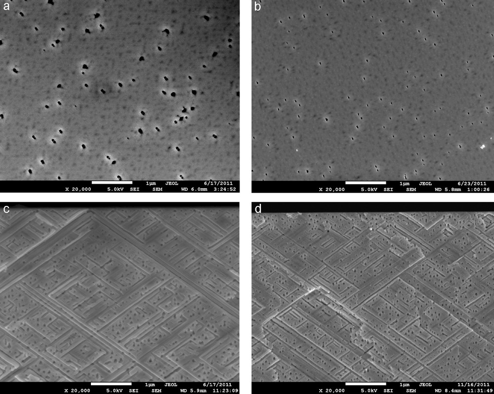
Scanning electron microscopy (SEM) image of the surface and cross-section of (100) GaAs substrate anodized for 150 s in HF-KI electrolytes with low concentration of HF (a) and (c) and high concentration of HF (b) and (d). The white scale bar corresponds to 1 μm.
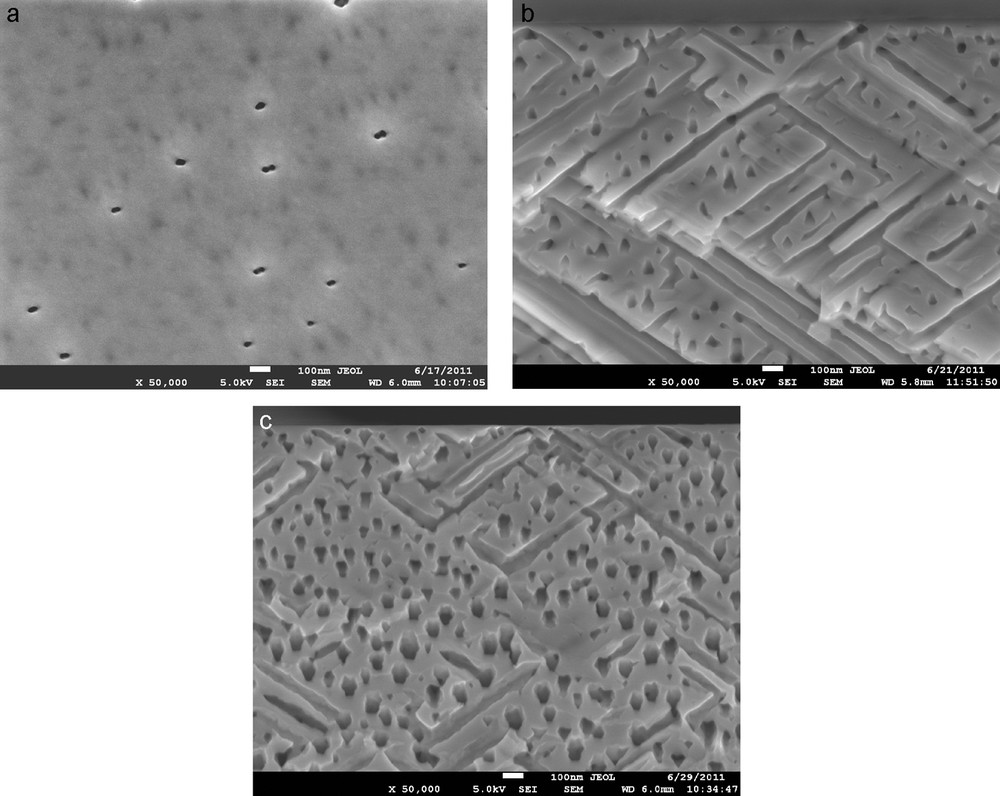
High-magnification scanning electron microscopy (SEM) images of (100) GaAs substrate anodized for 150 s in HF-KI electrolytes with low concentration of HF: a: plan view; b: cross-section of the substrate cleaved along < 01 1> direction; c: cross-section of the substrate cleaved along < 01–1 > direction. The total porous layer depth is 10 μm. The white scale bar corresponds to 100 nm.
The surface morphology was further investigated by AFM. Especially the sample prepared with a high HF concentration showed extremely low values of surface roughness between the nucleation sites (typically 2 nm). Even longer etching times resulting in the pore depth of several micrometers do not significantly deteriorate this value.
Relatively thick layers of InxGa1-xAs with varying In content were grown on GaAs porous substrates with different pore depths to investigate changes in the surface morphology and PL spectra allowing simple comparison of a large set of samples.
Fig. 3 shows a cross-section of the porous substrate from Fig. 2 overgrown by 400 nm of In0.2Ga0.8As at 560 °C with a ten-minute substrate treatment at 600 °C under AsH3 flow to remove surface oxides. The high-magnification image clearly demonstrates that at these temperatures, mass transport, which has significant impact on the epitaxy from the liquid phase on porous substrates [20], is greatly suppressed. Careful investigations show that originally hexagonal cross-section of pores acquires a more rounded shape. On the other hand, in the porous substrates treated at 700 °C, mass transport plays an important role and individual pores are transformed into hollow figures (Fig. 4c).
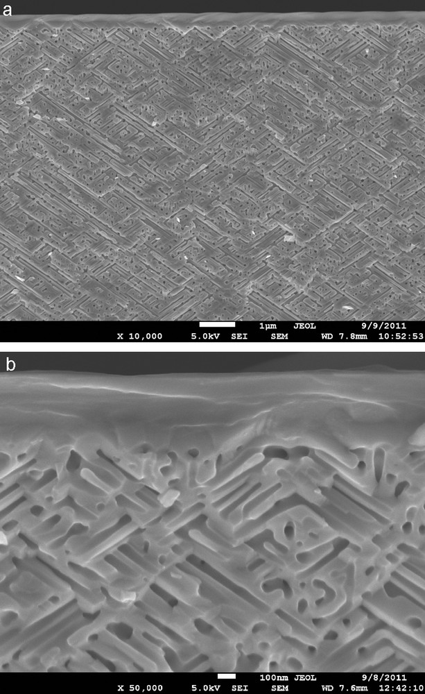
Cross-section of the porous substrate from Fig. 2 overgrown by 400 nm of In0.2Ga0.8As. The white scale bar corresponds to 1 μm (a) and 100 nm (b).

Scanning electron microscopy (SEM) images of a 1200 nm thick layer of InAs grown on a monolithic substrate (plan view) (a) and highly porous substrate (plan view) (b), (cross-section) (c).
On monolithic substrates a regular cross-hatch pattern with elongated ridges and valleys develops along < 110 > directions (Fig. 5a), while the morphology on highly porous substrates is similar to the one observed on homoepitaxial GaAs (Fig. 5b). Similar morphologies were observed on a 600 nm thick layer of In0.25Ga0.75As by NDICM (Fig. 6). NDCIM is limited by its lateral resolution, however, in comparison with SEM, allows to quickly observe large sample areas giving the proof of the layer uniformity on a macroscopic scale.
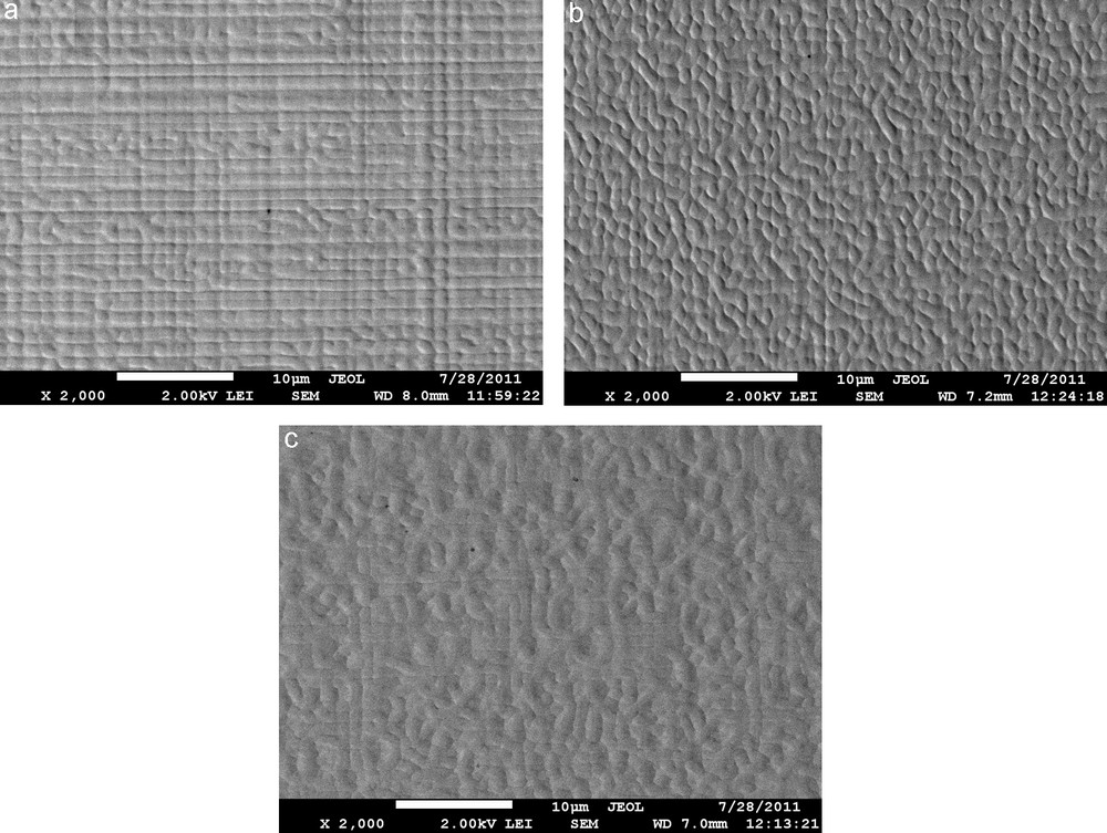
Plan view scanning electron microscopy (SEM) images of a 400 nm thick layer of In0.2Ga0.8As grown on a monolithic substrate (a), highly porous substrate (b), and weakly porous substrate (c). The white scale bar corresponds to 10 μm.
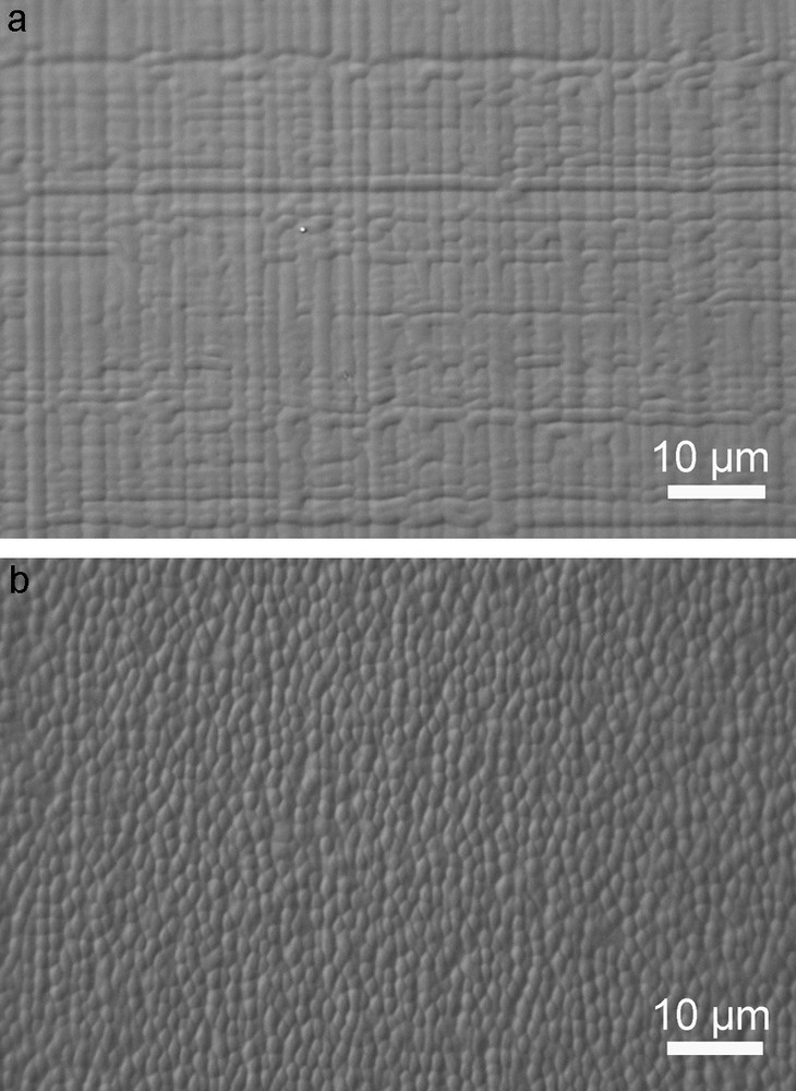
NDICM images of a 600 nm thick layer of In0.25Ga0.75As grown on a monolithic substrate (a) and highly porous substrate (b).
Twelve hundred nanometer thick In0.5Ga0.5As layers were grown at 560 °C with a ten-minute substrate treatment at 700 °C under AsH3 flow. Layers formed by mosaically arranged rather than continuous blocks with an irregular shape were observed on monolithic substrates (Fig. 7a), while a complex structure with more closely packed grains of 1–2 μm in size was observed on highly porous substrates (Fig. 7b).
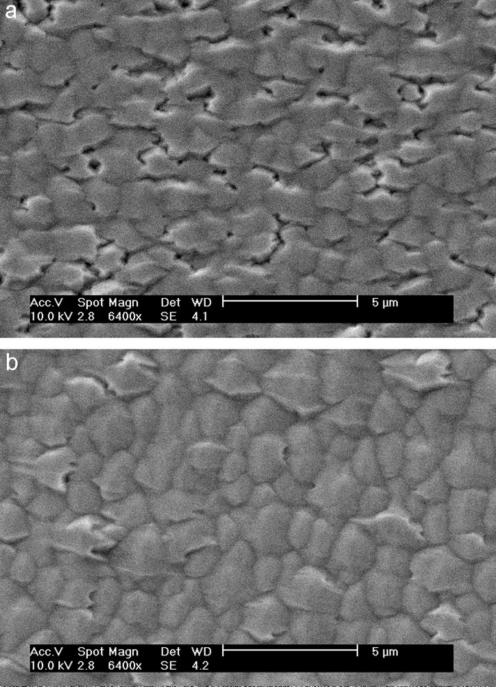
Plan view scanning electron microscopy (SEM) images of a 1200 nm thick layer of In0.5Ga0.5As grown on a monolithic substrate (a) and highly porous substrate (b). The white scale bar corresponds to 5 μm.
Twelve hundred nanometer thick InAs layers were grown at 560 °C with a ten-minute substrate treatment at 700 °C under AsH3 flow. The morphology was quite similar on both monolithic and porous substrates, yet the layers grown on porous substrates were more compact and systematically yielded higher integral luminescence efficiency. In general, nonradiative processes are associated with localized defect levels, whose presence is detrimental to material quality and subsequent device performance. The luminescence efficiency or the probability of radiative recombination is directly linked to the optical properties of the material and PL is a standard tool in evaluating its quality.
Fig. 8a compares low temperature PL spectra from InAs layers grown on three different porous substrates with a different porous layer thickness (631–610 μm, 638–635 μm, 641–643 μm) and on a monolithic substrate. The PL spectra were recorded with FTIR spectrometer equipped with liquid nitrogen cooled InSb detector under identical experimental conditions. The spectra have a composite character with at least three components. Fig. 8b presents the deconvolution of the PL spectrum from the sample 631 with four Gaussians. A consistent identification of the bands according to the known literature data is as follows:
- • the band peaking at 0.404 eV originates from band to Sn-acceptor transitions;
- • the band with maximum at 0.396 eV is due to donor-acceptor impurity band transitions;
- • the band at 0.384 eV correlates with the identification of PL from a deep impurity or defect related impurities;
- • with account to the uncertainty introduced by the deconvolution of the PL spectrum, we identify the band with the peak at 0.372 eV as LO-phonon replica (LO-phonon - 29.5 meV) of the band with maximum at 0.396 eV.

Low temperature PL spectra of InAs grown on three different porous and on a monolithic substrate (a) and deconvolution of the PL spectrum from sample 643 with four Gaussians (b).
4 Conclusions
Porous GaAs substrates with a high degree of porosity and periodicity with low density and size of nucleation sites and low surface roughness were prepared by electrochemical etching.
Layers of InxGa1-xAs with varying In content were grown on monolithic substrates and porous substrates with a different pore depth. Significant changes of the surface morphology and the enhancement of the photoluminescence efficiency were observed on porous substrates. These initial results indicate that the use of porous substrates could be developed into a general concept of defect reduction in heteroepitaxial growth with a large lattice mismatch.
Acknowledgements
The work was supported by the projects P108/10/0253 and P102/10/1201 of the Czech Science Foundation.