

1 Introduction
Since pioneering theoretical works in the 1970s, molecular electronics has attracted a growing number of academic studies. The rise in scanning probe microscopes and advanced lithographic techniques has allowed more and more refined experiments with an always better control of such challenging devices where a single molecule has to be trapped between two mesoscopic electrodes. Even if concrete applications still seem unrealistic in a near future, our knowledge on the electronic transport through organic or metallo-organic materials is increasing, what can be directly useful in organic electronics that offers interesting alternatives to semiconductors for displays, biosensors, smart paper, and so forth. Among the vast class of molecules that chemists can synthesize, molecular switches are particularly appealing as they can naturally mimic an electronic switch, or transistor, which is the basic unit of our day life electronics. The spin degree of freedom is also very interesting as it could be used for spintronics or quantum computing applications, with the advantage to be linked in a molecule to light atoms, that is, with a priori small spin–orbit coupling and therefore long spin lifetime. The spin-crossover (SCO) molecules combine those two properties and therefore show unique thermodynamical and dynamical behaviors that are actively studied by both chemists and physicists since more than 50 years, mainly in their bulk form. More recently, interdisciplinary projects have allowed one to decrease the size of study to nanoparticles, ultrathin films, and even single molecules. Such low-dimensional samples opened the way to study the electronic transport through SCO, which are mainly insulating in their bulk form.
The goal of this article is to review recent experiments dealing with electronic properties of SCO. It is divided in two parts. In the first one, techniques used to measure the current–voltage curve of a single molecule will be introduced. A particular attention will be paid on scanning tunneling spectroscopy (STS) where textbook examples will be described that will emphasize the different features observed in molecular electronics. The second part will be dedicated to a review of recent works measuring electronic properties of single SCO molecules, once again with a particular attention on STS experiments.
2 Measuring the electronic transport through a single molecule
The goal of this first part is to introduce the nonspecialist reader with typical experimental setups and theoretical background in the field of molecular electronics, more particularly measured by scanning tunneling microscopy (STM). Key articles in the field that have shown new concepts will be presented. Most of these articles deal with the electronic properties of simple atoms and molecules. Although the clear demonstration of some of these concepts has not been achieved yet on SCO molecules, we believe that the discussion of works that are now textbook examples on simple systems is important to better appreciate the recent results on SCO and to motivate new ones.
2.1 Introduction
The field of molecular electronics has been developed essentially with two main experimental techniques that enable to realize a gap of nanometer size between two metallic electrodes: break junction [1] (cf. Fig. 1a) and STM [2] (cf. Fig. 1b). Since the beginning the advantages and drawbacks of these techniques make them rather complementary, although they are coming from two rather different scientific communities (historically mesoscopic transport for break junction and surface physics for STM). In break junction experiments, the presence and the configuration of the studied molecule inside the gap is only an educated guess, based on the interpretation of I–V curves, in comparison with theoretical insights. The power of this technique comes from the fact that various important parameters can be varied like the gap size in mechanical break junction, the gate voltage in three-terminal devices, and more generally the temperature (down to mK) and magnetic field (up to typically 10 T). On the contrary, in STM, the presence and also the precise configuration of the molecule are very well known. But less external parameters are available, even if ultra-low temperature and high magnetic field setups are growing worldwide. Independent gate voltage is typically not available in a STM geometry. Temperature dependent I–V curves are also complicated to record because thermal drifts are more significant in STM and do not allow us to keep the very same molecule under the tip for a wide range of temperature. An important difference between the two techniques is also that in STM the two electrodes are not symmetric: one is a surface and the other a tip and in normal operation the coupling of the molecule is far stronger to the surface than to the tip. Few groups, however, use the STM in contact mode to mimic, in a much more controlled way, break junction experiments [3].
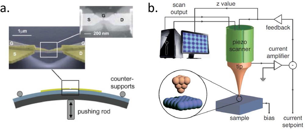
a) Typical mechanical break junction experiment (adapted from Ref. [4]). In this advanced geometry, a backgate electrode (G) can control the electrochemical potential of the molecule. The device is first realized using lithographic techniques and the gap between the source (S) and drain (D) is generally opened by electromigration. The fine control of its size, down to picometer, is done by mechanical motion through the pushing rod. (b) Typical STM experiment. The tip (or sample) is directly mounted on piezoelectric elements that control the gap size and the lateral position of the junction, down to picometer. An electronic feedback loop can keep constant the value of the tunneling current when scanning the sample, which is the basic operation mode of imaging (constant current image).
2.2 Break junction experiments
There are several approaches to make break junctions. The most simple one, which appeared the most recently, is to use a STM in a solution of the target molecules and to create dynamically the junction by crashing the tip into the surface (generally gold) and pulling it out at controlled speed (few nm/s) when recording the current at a given voltage [5]. Like for the well-known quantum of conductance experiment, plateau of conductance can be observed during the pulling out. This STM break junction (STM-BJ) technique looks rough but has been very powerful to measure reliably the conductance value of various molecules. The trick is not to focus on a single measurement but to record a statistical set of data, typically thousands. The histogram of conductance values therefore displays several peaks corresponding to the measurement through one, two, or more molecules in parallel in the junction. The relative broadness of these peaks is inherent to the change in configuration of the molecule and of the contacts at each new pulling try. The conductance of the molecule is defined by the position of the maximum of the first peak, that is, the most often measured value of conductance of the first plateau. I–V curves can be recorded by repeating the experiment for different voltages. This technique has been recently applied on SCO molecules [6] and will be discussed in the second part.
The classical break junction, or nanogap, is realized first by lithographic techniques to obtain a narrow constriction of a conducting stripe. The most commonly used metal is gold because of its inertness but platinum has been proved to be more stable with time at room temperature [7]. More recently graphene-based electrodes have also been tried [8], which can be of great interest for the selective grafting of organic molecules. Whatever the material, the gap can therefore be formed by passing high current density in the stripe that will thin and break by electromigration. One of the drawbacks of such a procedure is the possible presence of residual nanoclusters in the gap that can mimic a molecular behavior [9]. Another way to break a thinned wire is by mechanical pulling in a setup called the mechanical controllable break junction (MCBJ; see Fig. 1a). The interest of this latter is to control mechanically the gap size, what has been used, for example, to switch the spin state of a molecule with the applied strain [10]. A rather exhaustive review of such MCBJ setups with many examples is Ref. [11].
2.3 Principle of STM
In the following of this first part, we focus on STS, which combined with STM is certainly the more reliable technique to measure the electronic transport properties of a complex molecule in a known configuration. The principle of STM is first described. STM is based on the exponential dependence of the quantum tunneling current. The typical evanescent length scale of this current is with m the electron mass and the electronic workfunction, around 4–5 eV for metals. This leads to the rule of thumb that the current is decreasing by one order of magnitude when the gap size increases by 0.1 nm only, which is the cornerstone of the extraordinary spatial resolution of that technique. STM images are three-dimensional, recording the variation in the tip height when scanning in the plane of the sample (Fig. 1b). This is achieved by keeping the value of the current equal to a set point value (in the pA to nA range), thanks to a feedback loop that unfortunately limits the speed of the instrument to typically an image per minute. The simulation of a STM image is possible as the tunneling regime can be treated in perturbation theory [12]. The main parameters are recalled in Fig. 2a, which is a schematic drawing of a polarized tunnel junction.
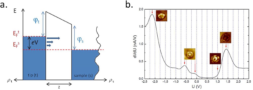
a) Schematic diagram of a tunneling barrier between two electrodes. (b) Spectrum of the differential conductance versus voltage for the tip above a C60 molecule adsorbed on a chromium surface. The images associated with the different features in the spectrum are conductance images recorded at the depicted energies.
When the gap size z is large compared to the evanescent decay length given previously, the tip and sample electrode wavefunctions can be considered as the ones of the free electrodes. The barrier height is often simplified to a single value, which is the average of the tip and sample workfunctions. In the standard convention, the voltage V is applied between the sample and the tip so that a positive voltage corresponds to a tip Fermi energy higher than the sample Fermi energy (cf. Fig. 2a), meaning that electrons from the filled states of the tip tunnel toward the empty states of the sample. On the contrary, for negative voltages the electrons come from the filled states of the sample. In the so-called Tersoff–Hamann model [13], the current can be written as
2.4 Tunneling spectroscopy through a molecule
It is now well established that STM and STS are powerful tools for the study of molecular electronics. However, the interpretation of data is generally not obvious and different phenomena can give rise to electronic signatures. Observing molecular states with STM is even paradoxical if one considers that the molecule is generally in strong coupling with the surface. Indeed, in the case where the coupling is strong, like for flat molecule lying on metals (e.g., pentacene on copper), there is neither clear electronic signature nor molecular orbital images [15], the molecular levels being strongly hybridized and broadened by the metallic continuum of states. In such a case, the molecular levels are pinned with respect to the sample Fermi energy and the standard measurement of the positions of the molecular states (hybridized with the surface) is done by recording the current derivative with respect to the voltage, the most often by a lock-in technique, with the feedback loop opened for the duration of the spectrum acquisition (typically few seconds). Indeed, considering the previous expression of the current, one can write, at constant z (with the assumption constant):
It is worth noting that this expression misses a second term that is considered to vary smoothly with the energy and therefore ascribed to a background. For small voltages with respect to the workfunction, it is generally assumed that the transmission is independent of the energy. This simple result shows that the local conductance is proportional to the LDOS, measured at the position of the tip, meaning in the evanescent part of the sample wavefunction. Fig. 2b shows an example of such a measure on a single C60 adsorbed on Cr(001) [16]. In the spectrum, the positions in energy of different hybridized molecular orbitals are clearly observed. The power of STM, as shown in Fig. 2b, is the possibility to make conductance images ( mapping) at the energies of interest to recognize unambiguously the different states, by comparison with calculations. Such images are, however, not always trivial to interpret as they are recorded with the feedback loop to scan over the molecule when recording its local conductance. C60 is a model molecule that has been widely studied on various surfaces by STM. Indeed, its spherical shape allows us to obtain a coupling that is sufficiently strong to pin its levels but not so strong to observe clearly the levels that are not too broadened by the continuum of states. For most of strongly coupled molecules (lying flat on the surface), the states are hardly distinguishable [17] and a trick consists in adding a decoupling layer (NaCl, Al2O3, etc.) between the sample and the molecule. In this case, molecular levels get narrower and appear clearly in the electronic spectroscopy [18]. The interpretation of data is, however, more complicated as the coupling between the molecule and the two electrodes can be of the same order of magnitude, with the consequence that molecular levels are not pinned anymore to any of the two electrodes. It has been shown experimentally that in such particular coupling conditions, called double tunnel barrier transport, the same molecular state can be measured in both polarities [19], at energy positions that depend on the detail of the voltage drop through the tunneling barriers. Moreover, in such a geometry, the tunneling is performed through its affinity or ionization levels in a neutral or charged state, giving rise to very different widths in the electronic spectroscopy for the different levels [20]. A clear experimental signature that distinguishes between a simple tunnel barrier and a double barrier model is the measurement of the level positions with respect to the tip height (coupling with the tip). In the first case, levels are insensitive to this parameter, whereas they can vary significantly in the second case. For SCO molecules, spectroscopic features coming from molecular levels are not clear cut and the coupling strength with the surface, that is, the question of the pinning of the molecular levels, has not been thoroughly addressed up to now. However, as will be discussed in more detail in the next part, recent studies have used spectra or images, in combination with calculations showing that the energetic positions of the molecular levels were spin state dependent, to discriminate both spin states [21,22].
2.5 Measuring molecular vibrations
Vibrational spectroscopy is a very powerful tool to identify molecular moieties that are widely used by the chemist community, generally by means of infrared spectroscopy. Electronic spectroscopy has also the ability to measure vibrational mode, with an unprecedented lateral resolution in the case of STS. The principle of such a measurement is explained in Fig. 3a. During the tunneling process, electrons can loose some energy by interacting with a vibrational mode. In contrary to the usual tunneling where the energy is conserved, there is a change in energy here that opens new conduction channels through the junction. Such a mode is generally called inelastic electron tunneling spectroscopy (IETS) by the STM community [23] and inelastic cotunneling by the break junction community [24]. Fig. 3b illustrates schematically the influence of those new conduction channels on the recorded spectra. In the standard differential conductance mode, it corresponds to sharp upward steps at the voltages (both positive and negative) that correspond to the energy of the vibrational mode. The amplitude of those steps is still challenging to predict but rarely exceed few percents of the total conductance [25]. The second derivative of the current with respect to the voltage, which can be also recorded by a lock-in technique, has the advantage to display clear peaks at the positions of the vibrational modes. Fig. 3c shows the first clear IETS result obtained with a STM on model acetylene and deuterated acetylene molecules adsorbed on a Cu(100) surface. The positions of the peaks have been found in very good agreement with other averaging spectroscopic techniques, what indicates that STM can give local and quantitative information on the molecular vibrational modes, at least the ones giving enough signal.
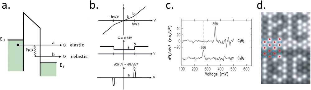
a) Drawing of a tunneling barrier including an inelastic process. (b) Schematic representations of the I(V), , and curves with a vibrational mode of energy . (c) Experimental IETS spectra on C2H2 and C2D2 molecules adsorbed on a Cu(100) surface. The peaks correspond to the C–H or C–D stretch modes that are shifted due to the mass ratio between H and D. (d) Conductance image recorded at the onset of the frustrated rotation mode of carbon monoxide (35 meV). Bright molecules are 13C16O whereas black one are 12C16O on Cu(111). CO molecules have been previously manipulated to display the 12C and 13C characters. IETS, associated with imaging mode, allows chemical identification at a molecular level (adapted from Refs. [23,26,27]).
The resolution of that technique is of course the one of STM, that is, few tens of picometer of lateral resolution. This allows us to distinguish two molecules with very close properties, like containing an atom of different isotopic mass, as shown in the textbook example of Fig. 3d on CO molecules. In the field of SCO molecules, such a technique can be of great interest as it is known that low spin (LS) and high spin (HS) species have different vibrational signatures [21].
2.6 Measuring a single spin
In the field of atomic and molecular magnetism, a key issue is to detect unambiguously the spin state of a single object. Few electronic signatures have been observed so far related to the spin. The first one is the Kondo resonance, which occurs at the Fermi level of the electrode in interaction with a spin impurity. This many-body electronic effect has been rationalized in 1964 by Kondo [28] to explain a minimum of resistivity in dilute magnetic alloys at low temperature. The main ingredients of the Kondo physics are a spin impurity coupled (coupling constant ) with a continuum of states (density of states at the Fermi level ). It can be shown that at less than a certain Kondo temperature , the spin of the impurity couples with the spins of the bath of electrons to create a singlet state. The spin of the impurity is therefore screened antiferromagnetically by the conduction electrons (Kondo cloud). Its spectroscopic signature is a sharp peak of density of states at the Fermi level that decreases strongly above . A zero bias anomaly has indeed been observed for the first time by STM on a Co adatom adsorbed on Au(111) (cf. Fig. 4a) [29]. However, the measured shape is not a simple resonance. Its interpretation required to introduce the concept of Fano resonance, which describes here the interference between different electronic paths, that is, tunneling either through the single impurity or directly to the continuum of states. The Fano lineshape can vary from antiresonance to resonance passing through curves similar to the one of Fig. 4a, by adjusting a parameter q, which is the ratio of the probability to path through the impurity over the probability to path directly in the continuum. In most magnetic adatom cases directly adsorbed on metals, q is found to be in the range from 0.5 to 4. However, when the spin impurity is somehow decoupled from the metallic surface, larger q values leading to almost lorentzian resonances are measured (cf. Fig. 4b) [30]. Note in this latter case that the width of the resonance, and therefore , is drastically reduced as is also reduced. Two experimental parameters can help to ascribe with more confidence a zero bias anomaly to a Kondo signature: magnetic field and temperature. Under high magnetic field (a few teslas at least), one can observe the splitting of the resonance [30]. Fig. 4b shows the temperature dependence of the resonance amplitude and width for a Co adatom on Cu2N/Cu(100). As already mentioned, the peak broadens and disappears rapidly above . The inset displays the extracted width with temperature together with a theoretical fit that allows us to deduce .
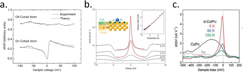
a) Differential conductance spectra with the tip over bare Au(111) and over a Co adatom adsorbed on Au(111). The zero bias anomaly is interpreted as a Kondo resonance and fitted by a Fano lineshape. (b) Differential conductance of a Co adatom on a Cu2N layer on Cu(100). The temperature dependence of the width at half-maximum (inset) is typical of a Kondo regime and determines the Kondo temperature (2.6 K in this case). (c) Differential conductance spectra recorded at the center of a Co phtalocyanine adsorbed on Au(111), either as deposited (CoPc) or dehydrogenated by tip pulses (d-CoPc). The latter shows a zero bias anomaly, which is interpreted as a Kondo signature, decreasing with temperature (adapted from Refs. [29–31]).
Such a Kondo peak has also been observed for various organometallic molecules adsorbed on metals. Such an observation should be limited to molecules having a spin state sufficiently coupled with the surface. Fig. 4c shows a textbook example of how the Kondo peak depends strongly on the fine details of the molecular coupling [31]. In this experiment, a Co phtalocyanine (CoPc) adsorbed on Au(111) does not show a zero bias anomaly at 5 K. On the contrary, after the dehydrogenation of eight H atoms surrounding the molecule by tip pulses, the dehydrogenated molecule (d-CoPc) shows a clear resonance, which decreases when increasing the temperature ( determined in this case). The given explanation is that the CoPc has a strong interaction that quenches its magnetic moment. For d-CoPc, the interaction is smaller and the Co atom recovers it spin 1/2, giving rise to the resonance. Surprisingly, the high is interpreted by a coupling that is still stronger than for Co adatoms on Au(111). A review on the Kondo resonances observed by STM on single adatoms is Ref. [32]. It is worth noting that, in STM experiments, the zero bias anomaly due to the Kondo physics has been the only spectroscopic feature related to a spin state measured on SCO molecules, as it will be detailed in the second part.
A more direct way to measure a spin state is to use IETS where the inelastic process is no more caused by a vibrational mode but by a spin-flip event. Typically, under magnetic field B, a system will show two levels separated by where the electron g factor is equal to 2 and is the Bohr magneton. It means that for an absolute tunneling voltage larger than , a new conduction channel opens leading to a step in the conductance. This technique, called spin-flip IETS, has first been demonstrated on single Mn adatoms adsorbed on two Al2O3 atomic layer patches on a NiAl surface [33]. It requires high magnetic field (few T) and low temperature (less than 1 K) because μeV/T. A typical spectrum recorded for different magnetic fields on a Mn adatom adsorbed on a decoupling Cu2N layer on Cu(100) is shown in Fig. 5a [34]. It is worth noting that such a measurement always requires that the spin state is decoupled from the electronic continuum of states. In Fig. 5a, one observes that even at zero magnetic field, a signal is observed. This zero field splitting is a direct measure of the magnetic anisotropy at the atomic level.
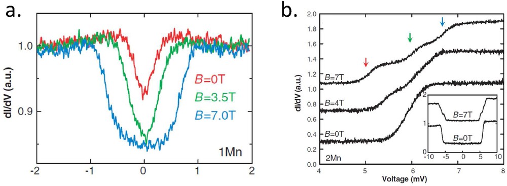
a) Differential conductance spectra on a single Mn adatom adsorbed on a Cu2N layer on Cu(100). The magnetic field–dependent inelastic signal is due to a spin-flip process between states ranging from to . (b) Differential conductance spectra on a dimer of Mn adatoms adsorbed on a Cu2N layer on Cu(100). The magnetic field dependence of the spectra shows that this inelastic signal comes from a change in the spin state, S = 0 to S = 1 (adapted from Ref. [34]).
Going further, this technique can also measure the exchange energy J needed to switch from a spin ground state to an excited state. Fig. 5b shows differential conductance spectra under different magnetic fields for a dimer of Mn adatoms on Cu2N [34]. The conductance step is now at higher energy (around 6 meV) that provides directly the measure of J. The definitive proof of such a measurement is the spectrum at 7 T where three clear substeps appear, which correspond to spin-flip processes between the level from to from . This spin-flip IETS has been applied already to single molecules (e.g., [35]) and recently to a Fe4 single-molecule magnet [36].
Another technique that is spin sensitive is the spin-polarized STM (SP-STM). The aim is to measure a tunnel magnetoresistance at an atomic scale by using a magnetized tip and a magnetized sample. Early demonstrations have shown magnetic domains of tens of nanometer size on Cr(001) [37] or Fe/W(110) [38], for example, and this technique is still very powerful in the study of nanometer scale noncollinear magnetic structures, like skyrmions. However, its subnanometer resolution allows us to measure single adatoms or single molecules, even if studies are more scarce. In a simple model of tunneling including the spin degree of freedom, it is possible to show that the magnetoresistive signal is proportional to the dot product of the tip magnetization (last atom of the apex) by the local sample magnetization [39]. However, this signal is generally small compared to the nonspin-polarized background (few percents) and depends on the energy. Every new system requires a spectroscopic study to determine energies where the magnetoresistive signal is measurable. Fig. 6a shows an ultimate example of the tunnel magnetoresistance measured on a Co adatom adsorbed on Pt(111) [40]. Such a single adatom displays a paramagnetic behavior, even at very low temperature and the measurement therefore requires magnetic field. Considering the tip magnetization constant during the magnetization cycle, the curves of Fig. 6a should be directly proportional to the projection of the adatom magnetization along the tip magnetization axis. The fitting of such curves allows us to deduce the local magnetic moment and anisotropy. It is interesting to note that, on contrary to spin-flip IETS, this technique does not require an electronic decoupling between the spin impurity and the continuum of states.
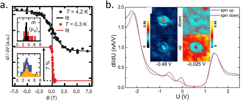
a) Differential conductance at 0.3 V vs magnetic field on a Co adatom adsorbed on Pt(111) recorded with a Cr covered tip for two different temperatures. The fits are based on a classical Langevin approach including magnetic anisotropy. The inset shows the histogram of values deduced for the atomic magnetic moment for atoms lying on two different atomic sites. (b) Differential conductance spectrum vs voltage on C60 molecules adsorbed on a Cr(001) surface recorded with a Fe covered tip. The blue and red spectra are recorded for molecules lying on domains of opposite local magnetization. The images in inset show conductance images of two molecules lying on different domains, at two different energies where they show a spin polarization (adapted from Refs. [16,40]).
SP-STM and SP-STS have been applied to single molecules, mainly to better understand the coupling between molecular states and a magnetized substrate [16,41–43]. The main result, shown for example in the spectra of Fig. 6b is that a nonmagnetic molecule, like C60, can display a spin-polarization for specific hybridized molecular levels [16]. These findings have an important impact on the interpretation of magnetoresistance measurements in organic spintronics, that is, with samples where the decoupling layer between the two magnetic electrodes is an organic layer. So far, to our knowledge, there is no SP-STM measurement dedicated to SCO molecules.
3 Recent experiments on single SCO molecules
3.1 Introduction
One advantage of using molecules in electronics and spintronics is the almost infinite possibilities to tune them at will to obtain new functional properties. In this respect, the fascinating properties of SCO molecules are particularly appealing to create new functionality in electronic devices. One can think, for example, at memristive behavior, light-induced switch, or strong magnetoresistive effects depending on the spin state.
Indeed, as demonstrated in 2003, the dielectric constant of SCO molecules depends on their spin state, which can be either increased or decreased depending on the molecules [44]. Since then experimental works have been devoted to measure the conduction of SCO molecules in the form of crystals, thin films, or nanoparticles. For example, devices containing a thin layer of SCO molecules show a charge transport modification depending on the spin-state of the molecules [45,46]. In the form of nanoparticles, conduction measurements on [Fe(trz)3(BF4)2] molecules present a conductance bistability depending on the temperature [47]. Depositing SCO nanoparticles on the top of 2D material like graphene also induces a modification of the electron mobility inside the graphene layer as a function of the temperature, with a clear change related to the spin state of the SCO nanoparticles [48].
From a theoretical point of view, although SCO molecules are studied from a long-time and there electronic structure is well known and correctly simulated by quantum chemistry codes with dedicated methods (such as the Becke three-parameter Lee–Yang–Parr hybrid (B3LYP) functional), the electronic transport through it has only been scarcely addressed, mainly because the bulk compounds are insulating. At the single-molecule scale, connected to two electrodes, theoretical studies have predicted a significant change in conductance between the LS and HS states [49,50]. For different FeII molecules, the calculation of the coherent electronic transmission through the d states leads to the same result: the HS state is more conductive than the LS state at low bias voltage. This effect is not only due to the molecular structural change but also related to the modification of its electronic structure. The lower crystal field amplitude in the HS configuration reduces the value of the highest occupied molecular orbital–lowest unoccupied molecular orbital (HOMO–LUMO) gap and therefore increases the value of the projected density of states at the Fermi level [50]. It is worth noting that majority (α) and minority (β) spins have a very different conductance, whereas the α conductance channels are blocked the β electrons are at the origin of the high conductance of the HS state [49].
Lefter et al. [51] wrote a review on charge transport and electrical properties of SCO molecules where more information can be found at the macroscopic and microscopic scale. In the following, we will focus on the works that have been carried on single molecules, studied either in solid-state devices/break junctions or by STS.
3.2 Break junction techniques
In break junctions, as seen in the first part, many external parameters like gate voltage, strain, magnetic field, temperature, and so forth can be applied to the molecule of interest. In the case of SCO molecules, most of these parameters have been used to realize and characterize an electronic switch that has been ascribed to a change in the spin state. Mainly two types of setup have been used, namely MCBJ and STM-BJ.
Using a three-gate terminal geometry allows us to apply a gate voltage that can in principle drive the SCO process. Indeed, for Mn2+ compounds (S = 5/2 or 1/2), adjusting the gate voltage induces a change in the spin state, directly measured by inelastic cotunneling under magnetic field. This change is related to the reduction in the terpyridine ligands what strengthens the ligand field. Moreover, interaction between the extra electron of the ligand and the LS of the Mn2+ gives a total spin state that can be either a singlet or a triplet state depending on the gate voltage [52]. The influence of a gate voltage on the spin state of molecules was also studied on FeII(L)2 (L = 4′-(4‴-pyridyl)-1,2′:6′1″-bis-(pyrazolyl)pyridine) molecules by experimental and theoretical studies. The measurement of a change in the spin state is less direct than in the previous case, as done only without magnetic field [53]. The signature of spin states is analyzed by the way of zero bias (Kondo) resonances. For an intermediate gate voltage, when the molecule is charged with an extra electron, lying on one ligand, the Fe2+ is believed to be in LS (S = 0), leading to an odd spin number that gives rise to a usual Kondo resonance. Increasing the gate voltage, the zero bias anomaly suddenly switches to a split resonance (cf. Fig. 7a and b). The interpretation of this behavior is that the double charged molecule (one electron on each ligand) has a Fe2+ in HS (S = 2), antiferromagnetically coupled with the spins of the two extra electrons. The overall S = 1 state shows level splitting by spin–orbit coupling, giving rise to the split Kondo resonance. Note that in these two cases of SCO controlled by a gate voltage, it happens always through the charging of the molecules.
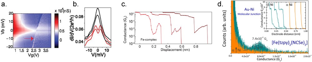
a) Differential conductance vs source–drain () and gate () voltages for FeII terpyridine compounds. The red arrow indicates the diagonal line due to the electrostatic environment modification. (b) Differential conductance traces as a function of for different (from top to bottom) 2, 2.4 (left hand of diagonal line), 2.9, and 3.3 V (right hand of diagonal line). (c) Three examples of conductance traces as a function of electrode displacement measured with the [Fe(tpy)2] molecules in a mechanical break junction. An increase in the conduction is observed as the signature of the LS to HS transition. (d) Conductance histograms for the paramagnetic [Fe(tzpy)2(NCSe)2] single-molecule transport in a STM-BJ under ambient conditions. The Ni tip magnetization is pointing upward (α, orange) or downward (β, green). The inset shows representative current vs pulling traces used to build the histogram. Adapted from Refs. [6,53,55].
In two-terminal break junction, the electric field applied in the junction can also be used to vary the geometry of the coordination shell and thus the molecule spin state. Harzmann et al. synthesized FeII compounds with two terpyridine ligands one being functionalized by the anchoring group to fix the molecule to the gold electrodes and the other with a push–pull system, which is very sensitive to an electric field. The stronger the dipole on the ligand will be, the more the octahedral geometry will be distorted by the electric field, thus inducing the spin state change. With a systematic study on different push–pull systems and metallic ions they demonstrate that for a strong enough dipolar moment the molecule will present a bistable conductance behavior. Typically, an applied voltage of about 1 V, which depends on the gap size, switches the molecule from a high to low conductance state, and vice versa for negative voltage [54]. A likely explanation is indeed that a SCO process is at the origin of this abrupt change.
The coordination sphere can also be deformed by stretching the molecules. For example, it has been possible by applying a strain in the junction to induce a uniaxial distortion of a S = 1 Co compound (Co(tpy-SH2) (tpy = 4′-mercapto-2,2′-:6′,2″terpyridine)). The consequence, measured by observing a splitting of a zero bias anomaly, is to modify the magnetic anisotropy [10]. Using Fe(tpy) (tpy = terpyridine) molecules, Frisenda et al. tried to demonstrate a SCO process with strain. They observed a nonmonotonous variation in the conductance with the distance in 56% of their junctions (Fig. 7c) that they ascribed to a change in the spin state, from LS to HS [55]. In STM junctions, mechanical SCO has also been attempted for Fe–porphyrin molecules. As calculated by density functional theory (DFT) techniques, once adsorbed on the surface, such molecules adopt a distorted saddle shape (in comparison with their gas phase geometry) that induces a spin S = 2. In the contact regime, one side of the molecule can be lifted from the surface and at a given tip–surface distance the molecule can have a planar geometry again and recovers its S = 1 spin state. Experimentally, a continuous sharpening of a Fano antiresonance is observed with the gap size, that is, when the molecule is pulled out from the surface by the tip that could be interpreted by a change in the Fe2+ magnetic moment [56].
Regarding spintronic properties of SCO molecules, experimental evidence is still scarce. Aragonès et al. recently realized experiments in STM junctions with single molecules attached between metallic surfaces (Au and Cu) and a Ni tip. They observed that for [Fe(tzpy)2(NCS)2] and [Fe(tzpy)2(NCSe)2] molecules the conduction through the molecular wire is larger when the molecules are in the HS state (at room temperature) than when they are in the LS state (at low temperature). In addition, they report in the case of both molecules in HS state attached to Au that the conduction in the molecular wire depends on the magnetic polarization of the Ni tip with a clear measurable conductance plateau when the Ni magnetization is pointing toward the surface and none for the reverse magnetization (cf. Fig. 7d). Interestingly, such a measurement is not intrinsic of the molecule but depends crucially on the nature of the substrate (possibly related to spin–orbit split surface states), as demonstrated by doing the same experiments on Cu(111) with no clear effect of the magnetization direction on the electronic transport [6]. Once the spin current polarization is generated at the interface, only the paramagnetic molecules can ensure its propagation as they favor minority spin carrier transport [6,49]. More recent experiments detail that the nature of metal atom in the SCO molecule is also of importance. Although [Co(tzpy)2(NCSe)2] on Au also shows magnetoresistive behavior, whereas [Mn(tzpy)2(NCSe)2] and [Ni(tzpy)2(NCSe)2] do not [57]. An important ingredient to get some spin filtering, as calculated by DFT, seems to be a rather strong hybridization with the surface, leading to spin polarized hybridized molecular states lying close to the Fermi level.
3.3 STS of SCO molecules
The main motivation to study SCO molecules with STM and STS is to better control the geometry of the molecule that appeared to be a key ingredient to understand its electronic transport properties and which is only a guess in break junction experiments. In most of the cases, STM easily achieves submolecular resolution on single molecules, or the determination of lattice distances in an array of molecules, what can be analyzed to determine almost unambiguously the molecular conformation on the surface. As for solid-state devices, the most difficult part is to discriminate between the spin states of the molecules adsorbed on the surface, both of them usually coexisting on the substrate. The assignation mainly relies on specific signature observed in the STS curves such as Kondo peak or vibrational modes as described in the first part of this review. To our knowledge, spin-flip spectroscopy under magnetic field, which is the most unambiguous way to determine the spin state, has not been performed yet on SCO molecules. It is, however, important to notice that the change in spin state is always related to a change in molecular conformation. In certain cases, this structural modification can be observed directly by STM, what helps and strengthens the assignation of the spin state.
To our knowledge, the first STM measurement on SCO was realized on [FeII(L)2](BF4)2 molecules (L = substituted bis(pyrazolyl)pyridine) deposited on a highly oriented pyrolytic graphite (HOPG) from a solution. They distinguished between both types of spin states randomly observed on the surface by STS measurements claiming that the LS state is more conductive than the HS state [58].
Fe(1,10-phenanthroline)2(NCS)2 (Fe–phen) molecules have been studied on different types of substrates. As single molecules, two types of conformations are observed once adsorbed on Cu(100), Cu2N/Cu(100) [60], Cu(111), or Au(111) [59], each one being assigned to one of the spin states of the Fe–phen molecules. As illustrated in the STS curves reported in Fig. 8a–d, zero bias anomalies are observed when the curves are recorded over the Fe–phen molecules in the configuration that is ascribed to the HS state. This assignation is coherent with the distance measured on the STM images between the phenanthroline lobes, this distance being larger for the molecule in the HS state than in the LS state (Fig. 8e and f). Depending on the substrate, the zero bias anomaly can be either a nonsymmetrical Fano resonance when the Fe–phen molecules are adsorbed on Cu(100), Au(111), or Cu2N/Cu(100) (red curves in Fig. 8a, c, and d, respectively) or a Fano antiresonance when adsorbed on Cu(111) (red curve in Fig. 8b) [59,60]. As expected, when recorded over the molecules in the LS state, no specific feature is observed in the STS curves (blue curves in Fig. 8) compared to the curves recorded over the bare substrates (gray curves in Fig. 8). In direct contact with the metallic surface the single molecules are trapped in their spin state and no SCO transition can be induced as the interaction between the molecules and the substrate is important. On the contrary, when an ultra-thin film of two monolayers is grown, the molecules in the second layer are partially decoupled from the substrate (Cu(100) and Cu(111)) and are in the HS state, as determined by the distance measured between the phenanthroline lobes. A smooth variation in this distance is observed when the bias voltage is increased, what could be interpreted as a thermally assisted SCO toward a LS state [59,61]. Passivating the Cu(100) by a Cu2N layer enables the manipulation of a single Fe–phen spin state. Indeed, the Fe–phen molecules are adsorbed in both spin states, the ones in the HS state exhibit a Fano resonance and have a larger conductivity than those in the LS state. By varying the voltage it is possible to change the spin state from the HS to LS at voltages greater than 1.1 V and from the LS to HS at voltages less than −0.8 V. The mechanism of the HS to LS transition was studied by measuring the switching rate at a constant voltage for different values of the tunneling current. It is found that HS to LS transition is driven by a single electron process, that is by the excitation of an electronic state, whereas the LS to HS transition is a higher order process involving eight electrons, ascribed to a vibrational heating [60]. Theoretical calculations confirm that the addition of a Cu2N layer decreases the coupling of the Fe–phen with the Cu(100) substrate, which enables the SCO transition [62]. Once adsorbed on Co islands grown on Cu(111), the Fe–phen single molecules are pinned in HS as identified by STS measurements over a large energy range (from −1.2 to 1 V) and calculations. Indeed, if in the calculations the LUMO of both spin states are at the same energy, the HOMO is around −0.9 V for the HS state when it is out of the investigated range for the LS state. Although the molecular Fe is not in direct contact with the Co, the molecular Fe ion is calculated to be strongly ferromagnetically coupled with the Co through the NCS ligands [63].
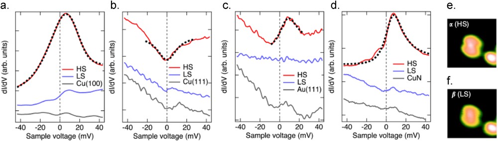
(a–d) dI/dV spectra recorded over single Fe–phen molecules in the HS state (red curves) and in the LS state (blue curves) adsorbed on different substrates, namely (a) Cu(100), (b) Cu(111), (c) Au(111), and (d) Cu2N/Cu(100). The gray curves have been recorded over the bare substrates. (e–f) STM topographic images of single Fe–phen molecules on Cu2N/Cu(100) in the (e) HS state and (f) LS state. Each image is 3.7 × 3.7 nm2 large and acquired at V = 0.1 V and I = 100 pA. Adapted from Refs. [59,60].
An other important family of investigated molecules on surfaces is the Fe(H2Bpz2)2L molecules (pz = pyrazolyl, L = bipyridine (bpy), phenanthroline (phen), or 3,4,7,8-tetramethyl-1,10-phenanthroline (phenme4)). On Au(111), the Fe(H2Bpz2)2phen and the Fe(H2Bpz2)2phenme4 molecules in direct contact with the substrate (submonolayer coverage) dissociate into a four-coordinate Fe(H2Bpz2) compound and the neutral L ligand [64,65]. But once adsorbed in second layer, the Fe(H2Bpz2)2phen molecules self-assemble to have the pyrazolylborate ligands pointing away from the surface [66]. The molecules are thus imaged as a three-lobe feature corresponding to the pyrazole groups. Both spin states have been ascribed by STS as the molecules in the HS state exhibit a smaller HOMO–LUMO gap than the LS ones, as calculated by DFT, and a Fano antiresonance at the Fermi level. It is worth noting that the coupling mechanism allowing a clear Kondo feature () for a molecule on a second layer is still unclear. The HS to LS transition can be induced by positive voltage pulses (bias threshold of 1.5 V) via a one-electron process. The LS to HS transition is obtained for bias voltage greater than 2.5 V, but contrary to the HS to LS transitions, molecules located at a distance up to 13 nm from the tip can be switched [66]. For Fe(H2Bpz2)2bpy on Au(111) a similar bilayer structure is observed [67]. The random contrast observed in the second layer is claimed to be because of the coexistence of both spin states, once again based on the argument that the HS state has a smaller HOMO–LUMO gap than the LS state. Surprisingly, the same contrast is observed in a large temperature range, from 130 to 300 K, in disagreement with the known SCO properties of the bulk compound.
Recent results have also been obtained on charged SCO molecules namely [Fe(pap)2]2+ molecules (pap = N-2-pyridylmethylidene-2-hydroxyphenylaminato) for which the central ion is a Fe3+ ion with a total spin of S = 1/2 in the LS state and of S = 5/2 in the HS state. The sublimation of these charged SCO molecules with their counterion () is possible but leads to the coexistence on the surface of both the [Fe(pap)2]2+ and the as observed on the Au(111) surface. To avoid the presence of the counterion, electrospray deposition [69–71] can be used to only select the charged Fe3+ compound. For both deposition methods, the same characteristic feature was observed in the STM images for the SCO molecules with and without the presence of the counterion. Once adsorbed on Au(111), different configurations of the [Fe(pap)2]2+ are observed without any evidence of the spin state [22]. To control the spin state of the molecules by voltage pulses, the [Fe(pap)2]+ molecules have been sublimated on Cu2N/Cu(100) leading to the observation of three molecular configurations (Fig. 9a–c) [68]. First, geometrical considerations of the relaxed structure of the free molecule obtained by DFT calculations have been used to assign the more distorted images (state A, Fig. 9a) to the molecule in the HS state. The two other conformations (states B and C, Fig. 9b and c, respectively) are assigned to molecules in the LS state. The main difference between the states B and C would come from different molecular orientations with respect to the substrate. It is worth noting that the counterions are believed to be adsorbed on some bare Cu area and therefore do not contribute to the interpretation of the measurements. In this case, no zero bias anomaly is observed, what is ascribed to the weak coupling ( smaller than the 4.6 K experimental temperature) between the molecule and the substrate. STS curves (Fig. 9d) recorded between −2 and +1 V over the three conformations present a dominant peak around −1.24 V. The molecules in states B and C present also an additional fainted peak at −0.14 V. The projected density of states over the Fe ion (Fig. 9e) only shows this additional peak for the molecule in the LS state, thus supporting the geometrical assignation. Interestingly, for this system, a rather fast reversible switching rate up to 7 Hz has been observed for sufficiently high voltage (2.5 V) between the three different configurations.
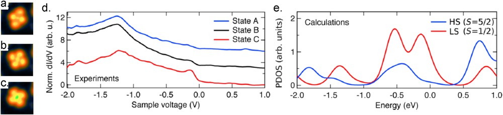
STM topographic images of the same [Fe(pap)2] molecule (a) in its initial state A and (b, c) in the switched states B and C, respectively. The STM images in (a–c) share the same color scale covering 0.21 nm and have the same width (2.8 nm). They were acquired at a voltage V = 0.1 V and a current I = 700 pA. (d) Normalized differential conductance spectra measured with the same tip over the center of the same molecule in states A, B, and C. The current feedback loop was opened at a set point of 1.2 nA and 1.0 V. (e) Calculated DOS projected on the Fe ion for the HS and LS state of the [Fe(pap)2] molecule. The zero energy corresponds to the HOMO energy of the LS state. Adapted from Ref. [68].
Finally, [FeII((3,5-(CH3)2Pz)3BH)2] (pz = pyrazolyl) molecules were investigated on the Au(111) surface [21]. They self-assembled in one monolayer high islands, which exhibit a superstructure at given voltages. Typically, at a bias voltage of 0.3 V, one molecule over three is appearing bright (Fig. 10a), whereas the complementary image is obtained at −0.7 V (Fig. 10b) thus showing that the molecules in the layer have different electronic properties. Complementary ab initio calculations revealed that the tunnel conduction is possible through the orbitals of the Fe ion and that the position of these orbitals with respect to the Fermi level depends on the molecular spin state. In other words, at positive bias voltage the conduction is higher through the molecules in HS state. This allows us to identify the superstructure as a mixed spin state phase with one molecule in HS state and two in LS state. Complementary IETS measurements show characteristic inelastic steps in the dI/dV curves acquired above the molecule in the HS state (Fig. 10c). Comparison with the theoretical calculations of the coupling between vibrational modes of the molecules and the -derived orbitals confirmed indeed that in this system the electron–vibron coupling is far stronger for HS than LS, giving a new spectroscopic feature for the assignment of the spin state. Interestingly, by coupling the STM with an external focused blue laser, it has also been possible to follow the SCO transition under light excitation and its relaxation to the mixed spin state phase.
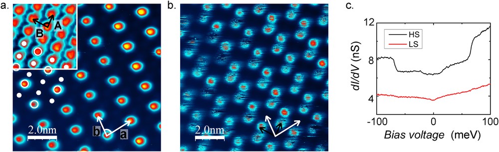
STM images acquired at (a) 0.3 V and (b) −0.7 V in constant height mode showing a mixed spin-state superstructure (). Inset of a topographic STM image acquired at −1.5 V showing the full molecular crystal. The full (empty) dots indicate the position of the dark (bright) molecules at 0.3 V. The black and the white arrows indicate the molecular crystal lattice parameters and the superstructure lattice parameters, respectively. (c) Low-energy curves for both types of molecules in the superstructure. Inelastic steps are visible in the spectrum recorded above the molecules in HS appearing bright at 0.3 V (black curve). No specific signature is observed in the spectrum recorded over the molecules in the LS state (dark at 0.3 V, red curve). Adapted from Ref. [21].
4 Conclusions
The recent experiments in break junctions and STM demonstrate the possibility to trigger the spin state of single molecules by external stimuli. For molecules in direct contact with a metallic electrode, the main challenge remains to identify the spin state of the molecules. Indeed, as observed by STM measurements, both molecular spin states are usually observed once the SCO molecules are adsorbed on a surface and STS measurements (with specific signature like Kondo peaks or vibrational modes) combined with ab initio calculations are mandatory to identify the molecular spin state. Moreover, the STM/STS measurements highlight the fact that the conduction of a given spin state strongly depends on the applied bias voltage. Expect from the recent results with polarized tip in a STM-BJ, no study focuses on the behavior of SCO in ferromagnetic junctions. One can expect that in a near future the possibility to realize STM measurements under magnetic field or with spin polarized tip will be investigated for single SCO molecules. One of the future challenges for the development of molecular spintronic devices is to design robust interface between SCO molecules and the metallic electrode to control the SCO process.
Acknowledgments
This work has received funding from the European Union's Horizon 2020 research and innovation program under grant agreement No. 766726. The authors warmly thank all their collaborators of the STM team at the MPQ Laboratory for fruitful discussions.