Introduction
Polyoxometalates (POMs) are molecular nano-oxides. Heteropolyoxometalates follow the general formula [XxMmOp]n−, where M stands for an early transition metal in its highest oxidation state (WVI, MoVI, VV) and X is a heteroatom from the p (Al, Si, P, As, Sb …) or d group, which is missing in isopolyoxometalates [1]. Some representative examples include the Keggin-type [PW12O40]3− and Wells–Dawson-type [P2W18O62]6− anions, based on which we have devised organic–inorganic hybrids. As molecular oxides, POMs are endowed with remarkable redox properties, combining the reducibility of bulk metal oxides and the high versatility of molecular species. They undergo successive and reversible mono- (or multi-) electronic reduction processes within a narrow range of potentials [2]. These properties are highly tunable/adaptable, according to the POM structure, its primo functionalization (see below) [3], the nature of the metallic addenda, and the nature of the counter cations [4]. In their reduced forms, POMs are commonly designated as electron reservoirs, and this has led to many applications in photo/electrocatalysis and energy conversion/storage [5, 6]. POMs are not only nano-oxides but also polyanions, and this makes them unique: their counter cations have important effects on various properties and play a crucial role beyond ensuring charge neutrality [7]. While POMs are traditionally prepared in aqueous solution as alkali or acid salts, their association with organic cations, such as alkylammonium, imparts their solubility in nonaqueous polar solvents. The cations drive POM organization up to the crystallization of POM-based architectures and materials. The redox potentials depend on the counter cations, the solvent, and other environmental effects. Small cations like Li+ and H+ allow to increase the charge stored in POMs [8]. In the solid state, the counter cations contribute to the adjustment of the energy levels of POMs relative to the Fermi energy of an electrode, modulating the conductivity [9].
As the missing link between extended oxides, commonly found in microelectronics, and conventional organic or organometallic molecules, POMs have attracted an ever-increasing interest in the field of nanoelectronics. They have been implemented in current-rectification devices [10], POM complexes of lanthanide single-ion magnets have been investigated as molecular spin qubits [11], and they have been introduced as charge storage nodes in hybrid molecular/semiconductor capacitors [12] and multilevel nonvolatile memories [13]. Crossbar arrays incorporating POMs embedded in polymer films or deposited onto graphene oxide have shown resistive switching behavior between a high resistance (OFF) state and a low resistance (ON) state [14], leading to memristive devices for neuromorphic computing [15]. Because they are molecules, implementation of POMs in molecular materials or devices requires a shaping process [16]. Depositing POMs onto electrodes is not an issue by itself since they readily physisorb on many. Yet in the context of molecular electronics, the control of their packing density and of their distribution on a substrate is a real issue that can hardly be tackled using physisorbed deposition. Avoiding the formation of aggregates, ensuring the uniformity of the layer to improve the properties and limit the variability from one device to the other is highly advisable. In this context, we have been exploring various strategies to immobilize POMs onto electrodes, with the aim of improving the control of the molecules/electrode interface that underlies the ultimate electrical properties and hence the device performance (the interface is the device) [17]. We have been investigating electron transport properties across POM-based molecular nanojunctions to figure out how the redox properties known from the solution state studies translate to the solid-state device. Additionally, we have demonstrated that we can commute the redox state of a POM layer by exposure to light or by applying an electric field. Our systematic approach will be revealed in the following sections.
1. POM-shaping process onto electrodes
As POMs are polyanions, their sublimation cannot be performed. Many examples of POM deposition onto electrodes rather deal with counterion exchange or entrapment in polymers. This is also at the basis of the elaboration of layer-by-layer materials [18, 19] with photo- or electrochromic properties [20, 21]. This strategy is easy to implement and we have used it to deposit the ring-shaped [H7P8W48O184]33− onto ultraflat template-stripped gold surfaces (TSAu) functionalized with a self-assembled monolayer (SAM) of 8-amino-1-octane thiol. This POM has been chosen for its high charge storage capacity (up to three reduction processes in the solution state, each corresponding to the injection of eight electrons). The experimental conditions of the dip-coating, incubation time of the TSAu substrate in a POM solution, and rinsing steps have been adapted to favor the formation of a uniform POM monolayer. The quality of the organic SAM on top of the substrate is also crucial to avoid the formation of aggregates. The successive steps of the deposition have been monitored by different techniques: (i) ellipsometry, which gives macroscopic thicknesses that should be consistent with the formation of monolayers (a few nanometers); (ii) atomic force microscopy (AFM) to qualify the homogeneity of the layers, their roughness, and spatial extension; (iii) polarization modulated reflection absorption infrared spectroscopy (PM-RAIRS) to recover the vibrational fingerprints of the organic SAM and that of the POM (Figure 1). The whole procedure has been extended to the deposition onto a large array of single-crystal Au nanodots [22]. Charge transport across the molecular nanojunctions has been probed by conducting AFM and the energetics of the molecular junctions discussed (as will be exemplified for another system below).
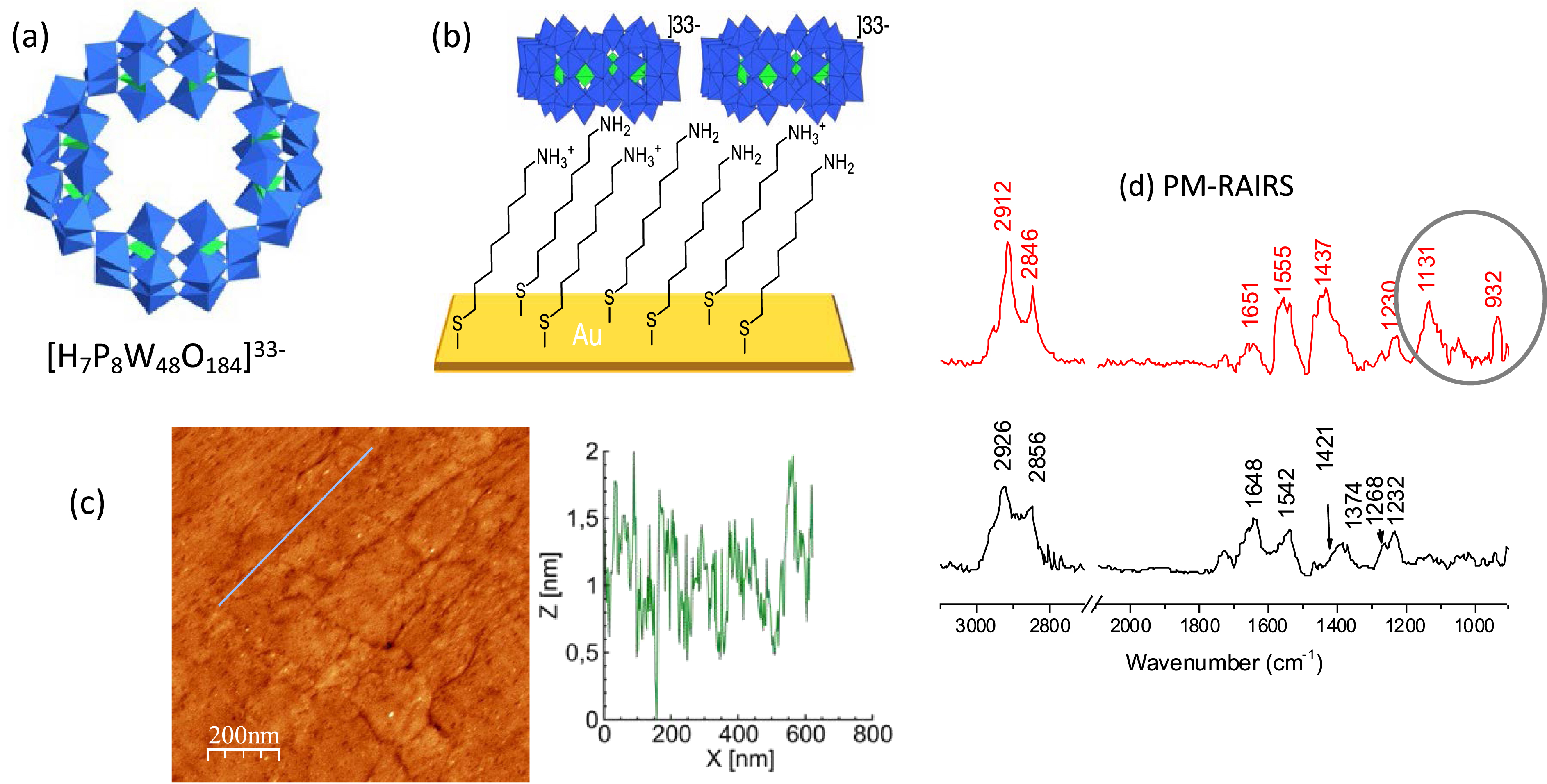
(a) Polyhedral representation of [H7P8W48O184]33− with WO6 and PO4 centers depicted by blue and green octahedra and tetrahedra, respectively; W atoms and P heteroatom located at the center and O atoms located at the apex of the polyhedra. (b) Scheme (not at scale) of the POM electrostatic deposition. (c) AFM image of the TSAu substrate after POM deposition with the corresponding height profile (following the blue line). (d) PM-RAIRS spectra before (black) and after (red) the POM deposition; the POM fingerprints are displayed in the highlighted region. Reproduced from Ref. [22] with permission from the Royal Society of Chemistry. Masquer
(a) Polyhedral representation of [H7P8W48O184]33− with WO6 and PO4 centers depicted by blue and green octahedra and tetrahedra, respectively; W atoms and P heteroatom located at the center and O atoms located at the apex of the polyhedra. (b) Scheme ... Lire la suite
We have also immobilized POMs onto carbon nanotubes (CNTs) through π–π interactions. This was achieved with a pyrene derivative of the Dawson anion, which was detected along the sidewalls of the single-walled CNTs by high-angle annular dark-field scanning-transmission electron microscopy [23]. This pyrene derivative belongs to the large family of covalent organic–inorganic polyoxometalate hybrids that we have significantly contributed to enrich [3, 24]. Our group has indeed devised systematic routes to the functionalization and post-functionalization of POMs, which give organically augmented POMs. We have particularly supplied organo-phosphonyl, -silyl, and -tin (or -germyl) derivatives featuring remote and reactive chemical groups. The primo functionalization provides simple and universal platforms, for example, bearing iodo-aryl groups, that can be further engaged to give more complex and bespoke post-functionalized species [25, 26]. Synthesis and subsequent reactions are generally carried out in organic solvents. In our case, the POM solubility is ensured by the use of tetrabutylammonium cations (TBA = N(C4H9)4+).
These POM-based hybrids offer a powerful alternative strategy for the covalent grafting of POMs onto electrodes or functional materials. Covalent bonding between the POM and the substrate indeed brings a higher control for the formation of a POM monolayer. Furthermore, extra POMs that would electrostatically or physically adsorb will be eliminated by thorough rinsing, possibly under sonication.
Covalent immobilization of POMs can be achieved either directly, thanks to the remote reactive group on the POM hybrid, or in two steps. The latter case involves a reaction between a POM hybrid and a substrate decorated with a SAM bearing a complementary reactive function. It has been exemplified with the classical peptide bond formation between carboxylic acid terminated SAM and amine or aniline terminated POM hybrid [27]. We have thus reported POM nanostructured gold substrates for biosensing [28, 29]. However, it is often hindered by a poor efficiency of the peptide bond coupling and related strong discrepancies in POM surface densities from one experiment to another [30]. This led us to favor the direct grafting of POM hybrids onto electrodes. Fine molecular engineering at the electrode interface is then attainable through the thoughtful choice of the remote/terminal anchor on the POM hybrid. We have reported that remote diazonium groups allow the POM grafting on a wide variety of substrates, ranging from carbonaceous materials [31, 32] to hydrogenated silicon [33], gold [34], or oxides [35]. Thiol, protected or not [36], and disulfide [37] are suitable for gold substrates [38] while carboxylic acid groups open the route to POM immobilization onto oxides, silicon oxide [39], and indium tin oxide (ITO) [35]. Furthermore, we will see below that given the choice of the anchor, the primo functionalization of the POM also imparts the charge transport. Finally, the nature of the covalent bond between the anchor and the electrode also impacts the properties of the materials [35].
Molecular chemists have thus plenty of room here to express their creativity for a fine-tuning of the resulting properties of the targeted functional materials.
2. Retrieving the POM signature from electron transport measurements in large-area molecular junctions
Once the POM layer is fixed at the electrode, charge transport across the layer has been assessed by closing the nanojunction either with a Hg-drop or the tip of an AFM set-up, in a vertical two-electrode configuration, akin to that used in metal/insulator/metal capacitors or memristive cells. Our first objective was to unravel the role of the POM in the charge transport.
2.1. Effect of the nature of the metal addenda Mo versus W [40]
We have reported the spontaneous dediazonation of diazonium terminated POM hybrids onto hydrogenated n-Si(100). The modified electrodes have been characterized by ellipsometry to support the formation of a monolayer and to assess its accurate thickness and by AFM to check the homogeneity of the surface coverage. Two similar POM hybrids of the Keggin type have been used, the only difference being in the nature of the metal addenda W or Mo: [PM11O39{Sn(C6H4)C≡C(C6H4)N2}]3− (M = W or Mo,
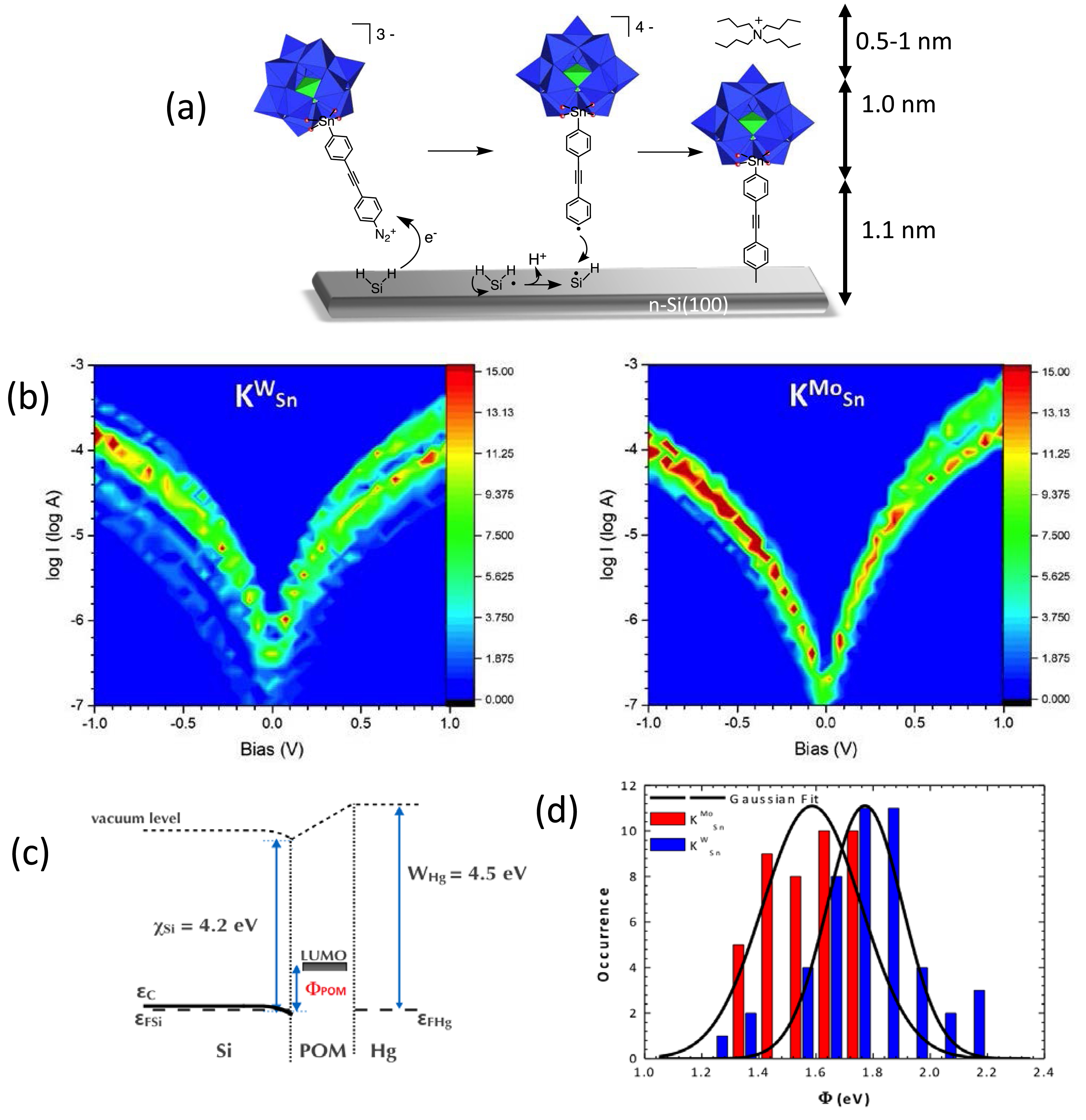
(a) The spontaneous grafting of diazonium terminated POMs onto hydrogenated n-Si(100). (b) Current versus voltage curves recorded with a Hg-drop electrode (semilogarithmic plot) on a monolayer of [PW11O39{Sn(C6H4)C≡C(C6H4)–}]4− (
(a) The spontaneous grafting of diazonium terminated POMs onto hydrogenated n-Si(100). (b) Current versus voltage curves recorded with a Hg-drop electrode (semilogarithmic plot) on a monolayer of [PW11O39{Sn(C6H4)C≡C(C6H4)–}]4− (
2.2. Effect of POM functionalization [39]
To enlarge the scope of our investigations, we have prepared two POM hybrids featuring remote carboxylic acid groups suitable for immobilization onto oxides: TBA4.4[PW11O39{Sn(C6H4)C≡C(C6H4)COOH0.6}] (
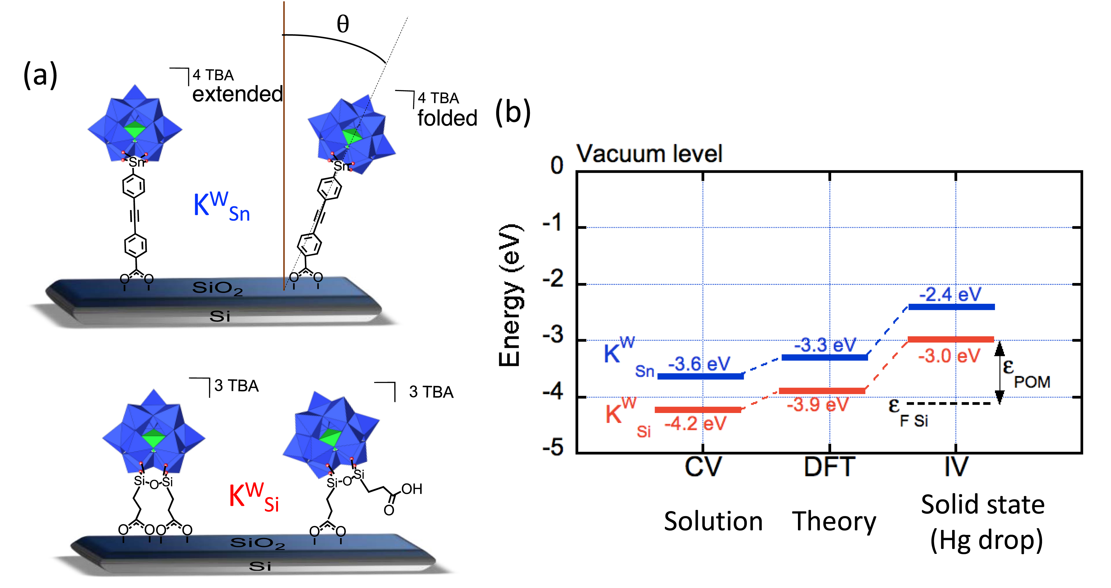
(a) Grafting modes of TBA4.4[PW11O39{Sn(C6H4)C≡C(C6H4)COOH0.6}] (
(a) Grafting modes of TBA4.4[PW11O39{Sn(C6H4)C≡C(C6H4)COOH0.6}] (
2.3. Counterion effects [48]
Most of the redox-active molecules involved in molecular junctions and resistive switching materials/devices are neutral [49], such as porphyrins, ferrocene [50], tetrathiafulvalene derivatives, oligothiophenes, and donor–acceptor systems [51]. POMs constitute a notable exception, and the associated cations offer a powerful lever to tune not only the POM redox properties but also the performance of the whole device. The introduction of coordination complexes in molecular junctions is less common, and the role of possible counterions is generally not assessed [52]. Yet, the presence of ionic species modifies the dielectric constant and the conductance by modulation of the internal electric field [53]. In redox-based random access memory, it has been proposed that when the molecular film becomes charged upon switching/variation of the redox state of its constituents, image/mirror charges form in the metal electrodes to maintain charge neutrality [54]. From the Marcus theory, in wet electrochemical environments, it is also known that the kinetics of the electron transfer is governed not only by the thermodynamics and the redox potential driving force but also by the underlying reorganization, including counterion rearrangement where applicable. Accordingly, the migration of the counterions in the molecular film was proposed to play a key role and to control the current–voltage (I/V) hysteresis characteristics of electrical bistability and hence of binary information storage capability [54]. The nature of the counterions, their size, polarizability, or mobility, for instance, is thus an important parameter in the molecular switch design [55], which has recently attracted attention.
We have thus prepared the Preyssler anion, [Na⊂P5W30O110]14−, with K+, H+, NH4+, and TBA+ counter cations. The POMs have been electrostatically deposited onto ultraflat template-stripped TSAu electrodes pre-functionalized with a positively charged SAM of 6-amino-1-hexane-thiol and the junctions have been closed with the tip of a c-AFM to record I/V curves (400–500 I/V traces have been recorded for reliable statistics). The mean I–V curves are plotted in Figure 4. At high voltages, the curves look very similar. Conversely, there is a clear discrimination at low voltages (−0.5 to 0.5 V), the current gradually increasing by a factor of 100 in the order K+ < NH4+ < H+ < TBA+, which is not predictable. Indeed, we could have expected the possibility of proton-coupled electron transport to enhance the conductivity, which is apparently not the case. Although it is commonly admitted that cations have an overall effect on the stabilization of the POM energy levels [9], it still remains difficult to predict their relative effect on the transport properties. Analyzing the I/V curves with the single energy level (SEL) model [56, 57, 58] (allowing to assess the energy position of the molecular orbital involved in the electron transport) gives the same order for the energy level positioning of the LUMOs, 𝜀0, K+ < NH4+ < H+ < TBA+. This is once again puzzling since the higher the 𝜀0, the lower the expected current. Another parameter, the electrode coupling energy Γ has to be taken into account (Figure 4d, one at each electrode). Γ reflects the hybridization between the molecular and electrode energy levels. These Γ parameters are included in the SEL model and have also been retrieved from the experimental data. Accordingly, the hybridization is stronger for the TBA+ cation, explaining the overall current increase trend. A full understanding of these experimental findings clearly requires a sound theoretical support. Meanwhile, we hypothesized that it could be discussed in terms of local dipoles at the molecules/electrode interface. Bulky TBA+ cations would lie mainly on top of the POM layer and build a large global dipole at the interface, which would induce a large vacuum level shift and then result in a large LUMO offset from the Fermi level. On the contrary, smaller cations—more in interstitial sites would create weaker dipoles—randomly distributed around the POMs result in a weaker, even negligible, average dipole at the interface, a lower vacuum level shift, and LUMO offset. In the solution state, counterions mediate the intermolecular electron transfer between two POMs [59]. A similar mechanism operating in the solid state would enhance the POM–cation–electrode coupling and explain the large coupling energy parameter Γ obtained for TBA+ cations. The hypothesis that the POM/electrode interaction depends on the nature of the cations is substantiated by a recent report of scanning tunneling microscopy images of individual POMs deposited onto Au(111) either by drop-casting (with TBA+ counter cations) or by soft landing from the gas phase with an electrospray ionization source (without any cation). The size of the electron cloud density has been found larger than the POM geometric size, disclosing some hybridization with the electrode, the effect being stronger in the presence of the TBA+ cations [60]. Finally, the modulation of the experimental conductivities we have observed probably reflects the competitive effects of the energy position of the LUMOs and the electrode coupling energies. This highlights the role of the counterion-dependent dipole at the POM/electrode interface and in molecule/electrode hybridization, which deserves further experimental investigations and extensive theoretical studies.
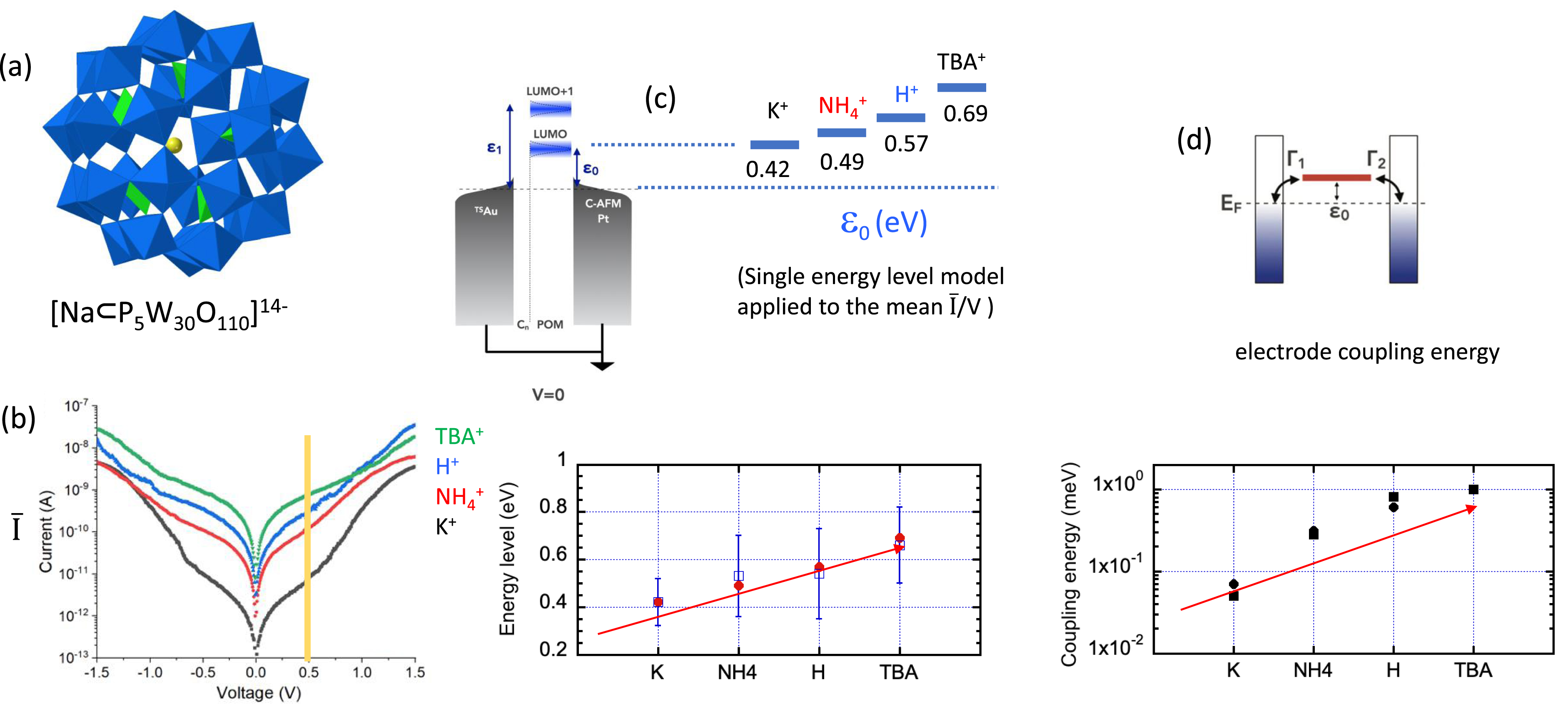
(a) Polyhedral representation of the Preyssler anion [Na⊂P5W30O110]14−. (b) Mean I–V curves obtained on TSAu–S(CH2)6NH2/POM//c-AFM tip nanojunctions (semilogarithmic plot). Effect of the counter cation type on the POM LUMO energy level position 𝜀0 (c) and Γ1 and Γ2 electrode coupling energies (d) obtained by simulation of the experimental I/V curves using the single energy level model. Reproduced from Ref. [48] with permission from the Royal Society of Chemistry.
3. Effect of the redox state and redox photoswitching [61]
Because of their multiple and readily accessible redox states, POMs are fascinating molecular species. Reduced POMs can be prepared chemically, photochemically, in the presence of an electron donor, or electrochemically. Comparing the conductivity of nanojunctions implementing the same POM but with different redox states seemed a relevant supplement to the scope of our investigations. Furthermore, manipulating the redox state of the POMs within a pre-formed monolayer would open the way to stimuli-responsive nanojunctions and would hence reinforce their attractiveness. It has been reported that the individual molecular redox states of a Lindqvist-type hexavanadate physisorbed onto Au(111) can be addressed by applying an external electric field. Single point scanning tunneling spectroscopy data have shown that the injection of up to four electrons resulted in a staircase increase in conductivity [62]. On the other hand, POM photoreduction is a well-known phenomenon that has been harnessed for the development of photochromic materials [63]. Indeed, the injection of electrons in the POM framework and their delocalization result in metal-centered d–d transitions and metal-to-metal intervalence charge transfer transitions that are responsible for the deep blue color displayed by most reduced POMs. However, because these electronic transitions have rather low intensities, POM-based photochromic materials generally involve thick or multilayer materials obtained by layer-by-layer deposition. We have thus decided to disclose the photocommutation of the POM redox state within a monolayer through a change in its conductivity. We have selected the Keggin-type polyoxomolybdate (TBA)3[PMo12O40] owing to the well-known ability of this compound to undergo photoreduction reaction under UV-irradiation. It is available in its fully oxidized state, referred to as POM(0), or in its one-electron reduced state, which can be chemically prepared to provide authentic samples of (TBA)4[PMo12O40] (POM(I)). In a control experiment, we checked that thick films of POM(0), obtained by drop-casting on a quartz slide, indeed turned blue under UV-irradiation. In the second step and to validate our approach, we have electrostatically deposited a monolayer of POM(0) or POM(I) on top of a Au substrate decorated by a 6-amino-1-hexanethiol SAM. This is a rare example of a molecular SAM built with open shell molecules [64]. The conductivity of the resulting nanojunctions Au-S(CH2)6-NH2/POM(0)//c-AFM tip and Au-S(CH2)6-NH2/POM(I)//c-AFM tip has been measured, and the mean current/voltage curves clearly showed an increase in conductance by a factor of about 10 upon reduction (Figure 5). The individual I/V curves have been fitted with a simple analytical SEL model (vide supra). A statistical distribution of the energy level values of the molecular orbital involved in the transport, with respect to the Fermi energy of the gold electrode, has been obtained for both junctions. The increase in the current observed for the POM(I) junction is thus proposed to be due to a lowering of the energy position of the main molecular orbital. The electron transport would thus be mediated by the LUMO (at approximately 0.6–0.7 eV above the Fermi energy, 𝜀F) in the case of POM(0) and the SOMO (single occupied molecular orbital) in the case of the radical POM(I) species, roughly aligned with 𝜀F. Possible involvement of the SUMO (single unoccupied molecular orbital, estimated at approximately 0.3–0.4 eV above 𝜀F) in the latter case should be supported by theoretical calculations. We then monitored the change in conductivity upon successively turning on and off an in situ UV-irradiation of the POM(0) layer. We expected the POM(0) layer to be reduced under light. After turning the light off, we let it in air, either at room temperature or under a moderate heating, to favor its reoxidation. The I/V curves were measured after each step. We observed a clear increase in the conductance upon irradiation, followed by a return to a state of lower conductance, similar to the initial one, after turning the light off. This is consistent with the behavior displayed by the monolayers of POM(0) and POM(I) just described above and leads to the conclusion that we were able to commute the redox state of the POMs at the monolayer scale.
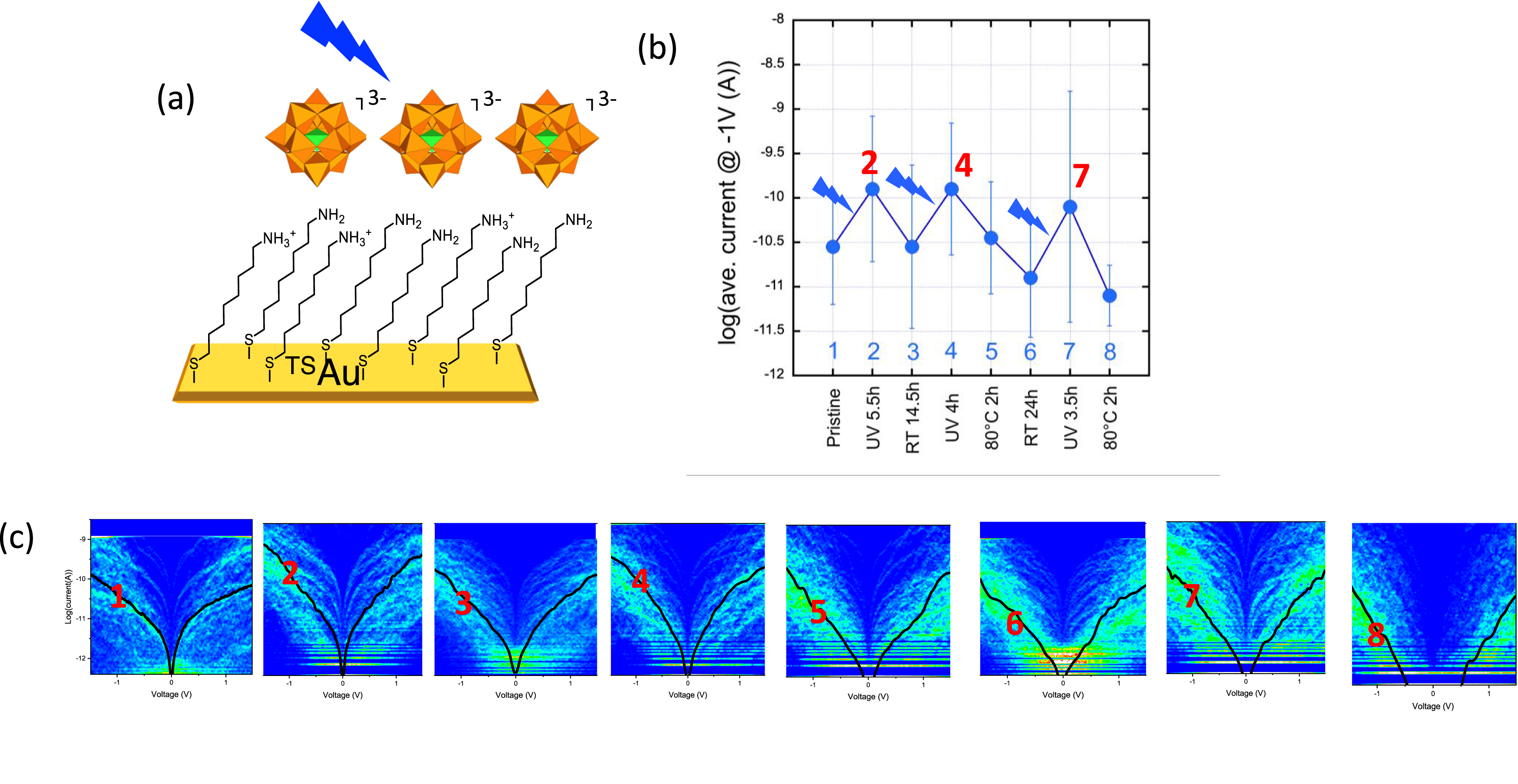
(a) POM electrostatic deposition on top of an 8-amino-1-octane-thiol SAM on TSAu. (b) Evolution of the mean current
(a) POM electrostatic deposition on top of an 8-amino-1-octane-thiol SAM on TSAu. (b) Evolution of the mean current
4. Towards resistive switching devices
In the studies previously described, a narrow bias window was deliberately chosen to protect the thin POM monolayer from any damage. In these conditions, we were not able to observe any resistive switching. In the case of bulk oxides, it is commonly acknowledged that the resistive switching mechanism is driven by the oxygen vacancies’ concentration and mobility [65], with the formation and disruption of conductive filaments. To emulate oxides and to allow the creation of conductive channels and gradient of charges, thick POM layers might be decisive. This prompted us to reconsider the use of POM functionalized with remote diazonium groups. Indeed, it is well known that upon electrochemical reduction, diazonium salts are prone to form multilayers covalently bonded to electrodes [66]. The deposition of POM monolayers from [PM11O39{Sn(C6H4)C≡C(C6H4)N2}]3−
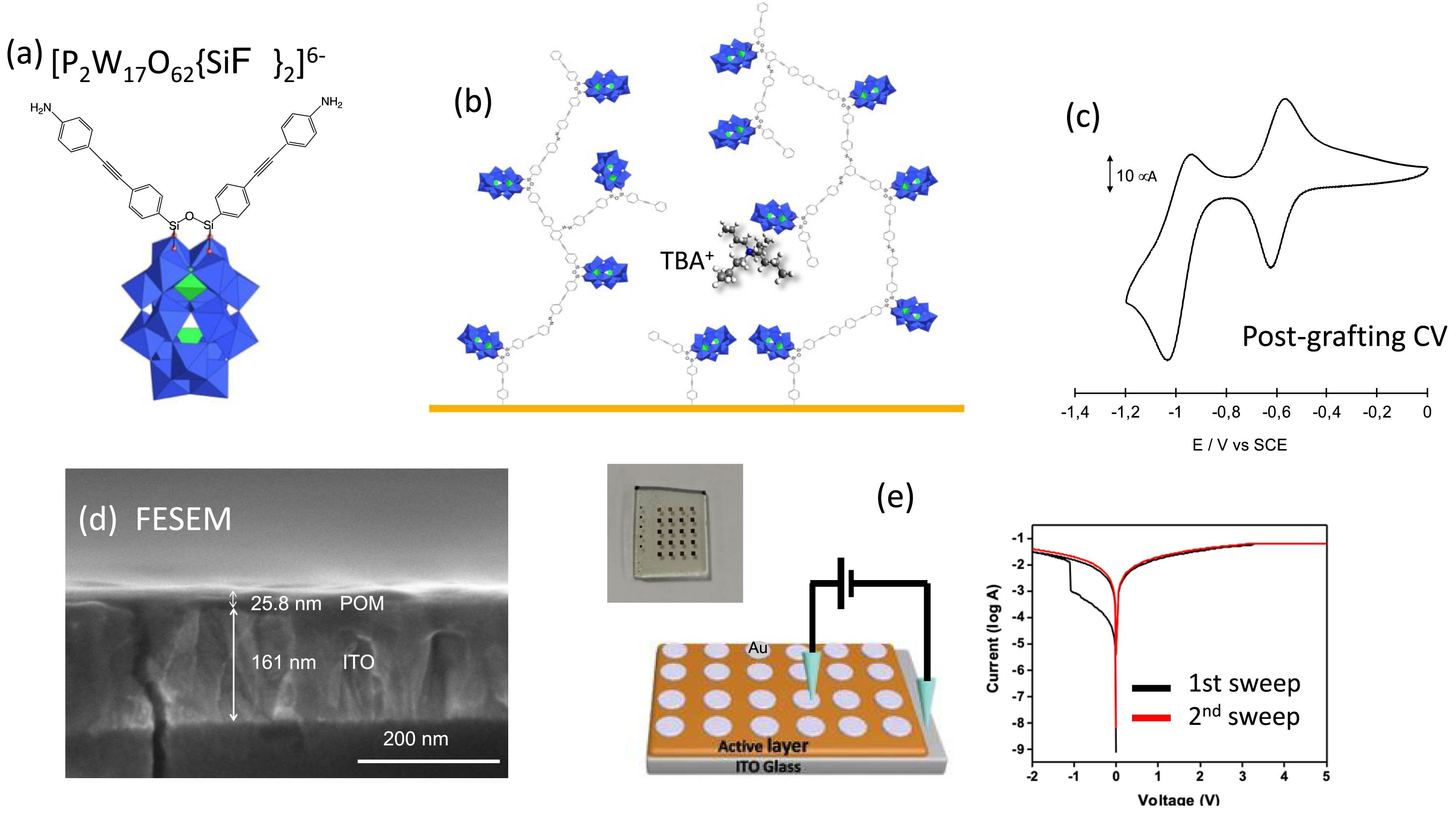
(a) Polyhedral representation of the bifunctionalized P2W17O61{(SiC6H4–C≡C–C6H4NH2)2O}] Dawson-type POM
(a) Polyhedral representation of the bifunctionalized P2W17O61{(SiC6H4–C≡C–C6H4NH2)2O}] Dawson-type POM
Oxide-based valence change memories play an important part in the development of memristive technologies for data storage, brain-inspired neuromorphic computing, data security systems, and mobile communications [69]. Crossbar arrays of substoichiometric tungsten oxide WO3−x memristors, viewed as artificial synapses, have been investigated as reservoir computing (RC) featuring internal dynamics and readout functions trained for handwritten digit or speech recognition as well as other classification and forecasting tasks [70]. Reservoir computing thus mimics the variability of neural connections in the brain. The key features to implement RC are variability, strong nonlinearity, and complex dynamic interactions. These have also been observed in self-assembled networks of molecular junctions, such as those built on azobenzene switches interconnected by Au nanoparticles and deposited on a several-electrode pattern [71]. The full potential of POMs for in-memory computing [72] and RC [73] has not yet been realized. To circumvent the intrinsically low in-plane conductivity of POM films, we have combined [PW11O39{(SiC3H6SH)2O}]3− POMs with Au nanoparticles acting as electrode relays. We have shown that the resulting POM/nanoparticle networks deposited on a six-electrode pattern display current variability and higher harmonic generation ability. Nonlinear interactions are also sources of low-frequency noise, which has been proposed to be indicative of RC performance. The 2D nanoparticle/molecule networks with the POMs displayed the highest low-frequency source noise among various tested molecules. The random telegram signal type noise detected has been ascribed to electron trapping/detrapping by the POMs [74, 75]. Currently, work is undergoing to improve POM-to-POM communication and in-plane conductivity of the molecular films. This will enlarge the scope of applications of POMs.
5. Conclusion and outlook
Scaling down the size of components to increase the memory density of electronic devices is no longer the main issue. The More-than-Moore applications include the integration of new functionalities in innovative/unconventional materials and a paradigm shift towards in-memory computing that mimics brain function. In this context, molecules still have their rightful place because they represent a unique combination of atomic structural precision, reproducibility, high tunability, and solution processability. Among molecules, POMs hold great promise because of their molecular diversity and the redox properties they share with oxides. This has prompted us to engage in a long-term project to underpin their potential in nanoelectronics. We have favored a step-by-step fundamental approach, and we have shown how to control the formation of densely packed POM monolayers on various types of substrates. We have investigated electron transfer kinetics to the POM monolayer and electron transport across the POM monolayers, revealing the POM signatures. We have also exemplified that POMs are stimuli-responsive molecules responding to light or to the application of an electric field. At this point, our experimental-based energy level diagrams outlining possible conduction mechanisms need to be supported by theoretical calculations to move ahead. As POM assemblies also involve their counter cations, the existence of electric dipoles and their possible reorganization or reorientation under an electrical bias or on POM charge trapping/detrapping and/or cation migration should be taken into account to gain a better understanding of the underlying mechanisms [76]. Polyanions thus offer a unique opportunity to investigate the effect of counterions, which has seldom and only recently been reported for other molecular junction/systems. This is a powerful lever that we will investigate further. Interestingly, artificial synapses based on peptide molecular junctions have been shown to be sensitive to cation flux, mimicking the behavior of Ca2+ or K+ in biosynapses. This has been attributed to the influence of cations on the electronic states of peptide molecules [77].
Declaration of interests
The authors do not work for, advise, own shares in, or receive funds from any organization that could benefit from this article, and have declared no affiliations other than their research organizations.


 CC-BY 4.0