1 Introduction
Simple inorganic pigments: titanium white, cadmium yellow and Prussian blue are known for centuries. The oldest in the family, Prussian blue (PB), was first described by M. Diesbach in 1704 [1,2]. Initially it was used as a blue pigment, but recently has found applications as a chemosensor [3], ion exchanger [4], in electrochromic displays [5], as molecular magnet [6], and in some semiconductor devices [4]. Two other materials studied here: titanium dioxide and cadmium sulfide are well known wide bandgap semiconductors, widely used as photocatalysts [7,8]. A special attention is paid to titanium dioxide as the material potentially suitable for solar energy conversion [9,10].
Photochemical properties of TiO2 surface modified with cyanometallates have been studied extensively [11–16]. Vrachnou et al. [11,12] found that the surface complexes show characteristic metal to metal charge transfer transitions (MMCT, FeII→TiIV) in visible range and excitation within new bands results in photocurrent generation. Other important contributions concerned composite materials consisting of titanium dioxide particles embedded in polymeric cyanoferrate matrices [17–20]. These materials showed some interesting properties—the photocurrent direction depends on the photoelectrode potential. This behavior was explained in terms of electrostatic barriers within the hexacyanoferrate matrix. Surprisingly, contrary to the reports from the Grätzel laboratory [11,12] the interactions between TiO2 particles and cyanoferrate matrix do not result in an MMCT (FeII→TiIV) absorption band and hence no sensitization of the semiconductor is observed. According to our knowledge there is no report on switching of photocurrent direction caused by change of the incident photon energy in similar systems. Similar phenomenon was reported for very different systems composed of helical peptides (attached to gold electrode) carrying various chromophores [21]. Systems described in this paper are much simpler, do not require organic electron donor neither acceptor and show photocurrents ca. four orders of magnitude higher.
Recently much attention is focused on chemical systems capable of performing logic operations [22–44], especially in solid state [25,45,46]. The research in the field of molecular logic is stimulated by natural limits of classical, silicon-based electronics [47]. This contribution describes new phenomena in systems containing semiconductor particles and hexacyanoferrate moieties, both as isolated ions and as polymeric films. The photoelectrochemical properties of the studied systems are interpreted in terms of chemical switches.
2 Results and discussion
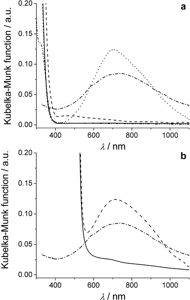
Modification of semiconductor materials with cyanoferrate complexes changes their optical properties: impregnation of TiO2 with [Fe(CN)6]4– ions results in the MMCT (FeII→TiIV) transition at 450 nm (Fig. 1a). This indicates formation of a stable “surface complex” containing the TiIV–N≡C–FeII(CN)5 moieties. Deposition of the Prussian blue layer on semiconductor surfaces results in materials exhibiting strong MMCT (FeII→FeIII) transitions, analogous to that of neat Prussian blue. These hybrid materials based on Prussian blue deposited on titania (Fig. 1a) or cadmium sulfide (Fig. 1b) are blue or green, respectively. PB deposited on SiO2 shows MMCT (FeII→FeIII) transition at 738 nm, while weak electronic interactions between semiconductor supports and the polymeric PB layer result in small hypsochromic shifts of the MMCT (FeII→FeIII) transition (λmax = 703 and 713 nm for TiO2 and CdS substrates, respectively). It is remarkable, that the absorbance of PB within the absorption band of the semiconductor is relatively poor.

Diffuse reflectance spectra of modified TiO2 materials and modifying compounds (a): TiO2 (––––––), [Fe(CN)6]4–@TiO2 (– – – –), PB@TiO2 (∙∙∙∙∙∙∙∙∙∙), PB@SiO2 (–∙–∙–∙–), and aqueous solution of K4[Fe(CN)6] (–∙∙–∙∙–, absorbance scale). Diffuse reflectance spectra of modified CdS materials and modifying compounds (b): CdS (––––––), PB@CdS (– – – –), and PB@SiO2 (–∙–∙–∙–).
To obtain information on the redox properties of electrons in the conduction band (and holes in valence band) quasi-Fermi level potential (EqF) measurements have been performed [48]. The method of Roy et al. [49] based on pH-dependence of the quasi-Fermi level potential was applied. Found values of EqF for TiO2, [Fe(CN)6]4–@TiO2 and PB@TiO2 at pH 7 are –0.80, –0.70 and –0.47 V vs. Ag/AgCl, respectively. The EqF value for CdS and PB@CdS are –0.38 and –0.0 vs. Ag/AgCl, respectively (Fig. 2). It should be noted that EqF shifts cathodicaly with increasing pH by 59 mV per pH unit in the case of titania-based materials and by 30 mV in the case of cadmium sulfide-based composites [49].

Positions of valence and conduction band edges of tested materials.
Voltammograms of ITO electrodes covered with appropriate materials were recorded in the dark and upon irradiation with chopped monochromatic light (Fig. 3). An electrochemical wave at E1/2 = 0.26 V vs. Ag/AgCl recorded for [Fe(CN)6]4–@TiO2 material is characteristic for the reversible [Fe(CN)6]3–/4– redox pair. Similarly, a quasi-reversible wave at E1/2 = 0.19 V was observed for PB@TiO2 and PB@CdS composites. The kinetics of photocurrent evolution agrees with generally accepted models [50].

Dependence of photocurrent generated on [Fe(CN)6]4–@TiO2 photoelectrode on applied potential (a; λ = 350 nm) and excitation wavelength (b; E = 0 V vs. Ag/AgCl). For comparison, the voltammogram in the dark of the [Fe(CN)6]4–@TiO2 electrode is shown (a, dashed line). Arrows indicate opening of the shutter.
Typical examples of voltammogram recorded upon chopped light irradiation (λ = 350 nm) together with photocurrent profile at constant potential (E = 0 V) for [Fe(CN)6]4–@TiO2 are presented in Fig. 3a, b, respectively. At the potential of 0.18 V the reduction of FeIII to FeII takes place. At the same point the photocurrent character changes from anodic to cathodic. Similar switching is observed for PB@TiO2 and PB@CdS at 0.25 and 0.13 V, respectively, when the wavelength of incident light is 350 nm.
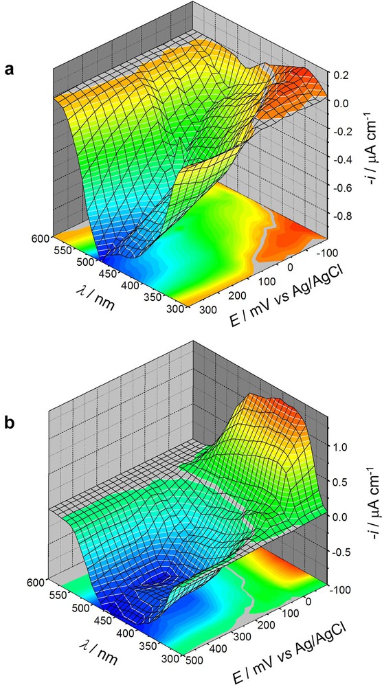
In a certain range of potentials the electrodes made of [Fe(CN)6]4–@TiO2 and PB@CdS show another interesting feature. The photocurrent switching between anodic and cathodic can be realized at constant potential using different wavelengths of the incident light (e.g. Fig. 3b). Depending on the electrode material and the potential the switching can be observed at 320–420 nm. In some cases there are two switching points. For instance, in the case of [Fe(CN)6]4–@TiO2 at E = 0.10 V the first switching (cathodic to anodic) appears at 325 nm and the second one (anodic to cathodic) at 400 nm. In order to have a full overview of the photocurrent generation as a function of applied potential and irradiation wavelength the measurements have been performed by recording photocurrent action spectra (with 10 nm step) at constant potentials. The spectra were collected at every 50 or 25 mV. In this way 3D pictures (phase diagrams or maps) were obtained (Figs. 4 and 5). In these studies, photocurrent values have been read as a difference between the steady-state current measured upon irradiation and the current in the dark just before opening the shutter. Photocurrent values used for the maps construction are not corrected for changes in incident light intensities with irradiation wavelength. The maps allow to make an analysis of the logic states (photocurrent) of the system upon application of various stimuli (vide infra).

Photocurrent profiles for cadmium sulfide photoelectrodes: neat CdS (a), PB@CdS (b).

Photocurrent profiles for titanium dioxide photoelectrodes: neat TiO2 (a), PB@TiO2 (b), [Fe(CN)6]4–@TiO2 (c).
Cadmium sulfide yields an anodic photocurrent upon irradiation within the whole absorption spectrum of the semiconductor except of very negative potentials, where irreversible reduction of the material takes place (Fig. 4a). Modification of the material with a thin layer of Prussian blue changes the absorption spectrum (vide supra), but the photocurrent action spectrum is not changed qualitatively when positive potentials are applied. At more negative potentials, however, significant cathodic photocurrent is observed (Fig. 4b).
Titanium dioxide generates an anodic photocurrent upon irradiation within the whole absorption spectrum (Fig. 5a). Impregnation of titanium dioxide with hexacyanoferrate(II) results in changes of absorption spectrum and photoelectrochemical properties. At positive potentials this material behaves like neat TiO2, but at potentials at which the iron complex is reduced to the FeII form a new feature appears (Fig. 5b). Ultraviolet irradiation still generates the anodic photocurrent, while irradiation within the MMCT (Fe2+→Ti4+) results in the cathodic photocurrent. The wavelength, at which the switching is observed, depends on the photoelectrode potential. At more negative potentials only the cathodic photocurrent is generated irrespectively on irradiation wavelength. Titanium dioxide modified with Prussian blue has the same photocurrent profile at positive potentials, but reduction of FeIII to FeII within the polymeric film results in immediate switching of the photocurrent direction (Fig. 5c). Again, the photosensitivity window is extended towards longer wavelength, but the photocurrent intensity in visible range is very low.
Photogeneration of cathodic photocurrents by n-type semiconductors were observed also in the case of indium and nickel hexacyanoferrate–titania composites [19,20], neat [51,52], chromium- [53] and nitrogen-doped titania [54], cadmium sulfide [55,56], cadmium telluride [57] and selenium [58] photoelectrodes.
2.1 Switching mechanism
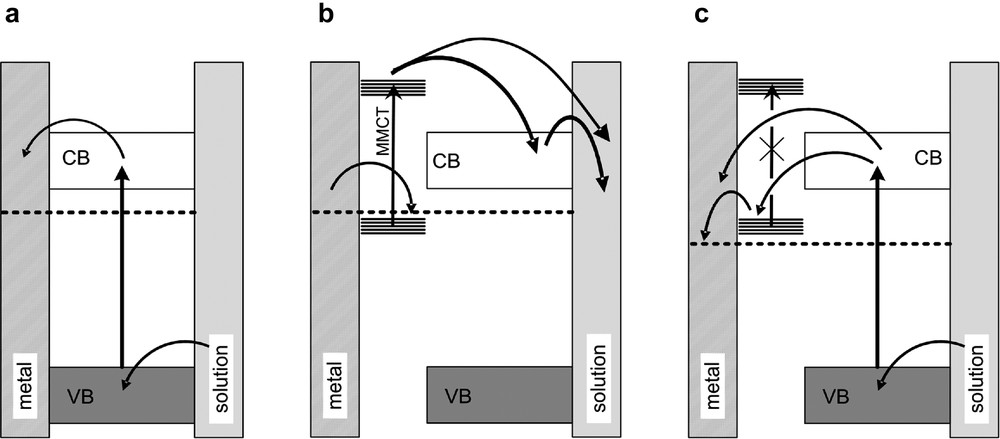
Collected data allow elucidation of the photocurrent switching mechanism caused by electron and/or photon energy changing. Fig. 6a shows a simple picture of the anodic photocurrent generation. The position of Fermi level below the conduction band edge constrains the cathodic photocurrent. The photocurrent action spectrum of the surface modified TiO2 depends on the potential applied to the electrode: at higher potentials it is identical with the action spectrum of neat titanium dioxide, while at lower potentials the spectrum extends towards visible range. Modification of the surface with the FeII complex results in formation of a new energy level between the valence and the conduction bands as expected from comparison of EFeIII/FeII with EqF of studied materials. Light absorption by the reduced complex (FeII) results in excitation of the surface species with concomitant formation of an unoccupied level within the bandgap of TiO2 (hν < Ebg, Fig. 6b). If this level lies below Fermi level, as in Fig. 6b, the electron transfer from the conductor occurs and a cathodic photocurrent is observed. Electrons from the excited state of the surface complex are transferred to the electrolyte solution directly or through the conduction band of the semiconductor. When shorter irradiation wavelength is applied a direct excitation of the semiconductor is possible (hν > Ebg). In the case of n-type semiconductors (CdS, TiO2) the anodic photocurrent is observed unless the potential applied to the electrode is lower then the conduction band edge (flatband potential). Application of more positive potential to the electrode may shift the Fermi level below the iron(II) level (Fig. 6c). Under these conditions the surface complex is oxidized to FeIII and its previously described excitation is not possible any more. Photocurrent can be generated only upon irradiation of the electrode with photon energy equal or higher than the semiconductor bandgap energy. This process is followed by the electron transfer in the direction of the conductor, as shown in Fig. 6c.

Mechanism of the PEPS effect – The electronic factor: generation of the anodic photocurrent by unmodified semiconductor (a); generation of the cathodic photocurrent by surface modified semiconductor in reduced form (b); generation of the anodic photocurrent by surface modified semiconductor in oxidized form (c).
This mechanism of photocurrent switching from anodic to cathodic caused by the potential change (energy of electron) can be valid for any semiconductor modified with complexes (or ions) which support an additional redox potential higher than the flatband potential. It applies to TiO2 and CdS materials modified with [Fe(CN)6]4– and Prussian blue complexes.
In order to understand the mechanism of optical switching the geometry of the surface modified semiconductor particle should be considered. The depth of photon penetration depends on the photon energy and absorption spectrum of the material (Fig. 7). Irradiation within the absorption band of the surface complex does not affect the inner part of the semiconductor particles and only the electron transfer processes presented in Fig. 6b may take place (cathodic photocurrent). The surface layer is transparent for photons of higher energy (compare absorption spectrum of the surface) which are absorbed by the nearly unmodified core of the semiconductor particle. The inner part of the material grain is responsible rather for the anodic photocurrent and therefore at shorter wavelengths this effect is observed. A potential applied to the electrode influences the form of surface complex (reduced or oxidized) and therefore its absorption properties. It changes, in turn, the position of the switching point because the nature of the dominant absorbing species changes. The net photocurrent depends therefore both on photon energy and applied potential. In the case of partially reduced semiconductor particle (e.g., CdS) light absorbed by the surface may also generate cathodic photocurrent, what leads to two switching points within the photoaction spectrum.

Mechanism of the PEPS effect – The optical factor: absorption spectra of the inner and outer layers of surface modified semiconductor particle and corresponding depth of light penetration.
The effect of photocurrent switching as a function of photon energy was not described for systems based on wide bandgap semiconductor particles until now. Due to two main factors affecting the net photocurrent effect, i.e. photon energy and potential, we propose to name this phenomenon as PhotoElectrochemical Photocurrent Switching (PEPS) effect.
2.2 Logic analysis
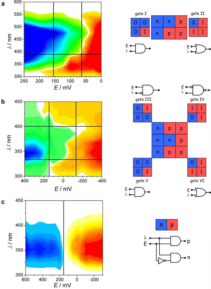
The photoelectrochemical switching in the systems containing different combinations of studied pigments is a good basis for construction of chemical logic gates. In principle, any chemical system which can exist in at least two stable or metastable states can be regarded as a molecular switch [23,25]. If there are more than one switching stimuli (here wavelength of incident light and photoelectrode potential) the system constitutes a good model for the logic gate or even more complicated logic system [23,34]. The Prussian blue-modified cadmium sulfide generates anodic photocurrent at sufficiently high potentials (E > 0.20 V) irrespectively on wavelength and cathodic photocurrent at low potentials (E < 0.05 V). Within the 0.05–0.20 V potential window the current direction depends on irradiation wavelength. Light of higher photon energy (325–400 nm, depending on potential of the electrode) generates cathodic photocurrent, while visible light generates anodic photocurrent. One can arbitrarily assign the two types of photocurrent to different logic states, for example anodic to logic 0 (low state) and cathodic to logical 1 (high state). The phase diagram of the semiconductor photoactivity can be therefore divided into zones according to the dominant photocurrent direction. This is schematically shown in Fig. 8a. The diagram consists of six zones; in order to simplify the logic behavior of the system it can be divided into two four-zone (2 × 2) subdiagrams (truth tables), marked as ‘gate I’ and ‘gate II’, respectively. The same can be done with switching stimuli: potential and wavelength. For every subdiagram the higher potential window was assigned to logic 0 and the lower potential window to logic 1. In analogous way the lower and higher wavelength regions were assigned to logic 0 and 1, respectively. In this system the left subdiagram is equivalent to the AND logic gate and the right one to the OR gate. This simple chemical system works like two basic logic gates depending on the photoelectrode potential window. Electronic equivalents are shown in Fig. 8a (AND gate and OR gate).

Maps of photocurrent generation for Prussian blue coated cadmium sulfide (a); [Fe(CN)6]4– modified titanium dioxide (b) and Prussian blue coated titanium dioxide (c) photoelectrodes. Corresponding truth Tables and equivalent electronic circuits are shown. Yellow to red colors correspond to the cathodic photocurrent, green to blue to the anodic photocurrent.
More complex behavior is observed for the [Fe(CN)6]4–@TiO2 system. The phase diagram of photoreactivity is divided into nine zones of different photoactivity, which gives four different 2 × 2 subdiagrams (Fig. 8b). The assignment of logic parameters is identical as in the case of PB@CdS system. The four subdiagrams manifest four different logic devices that can be mimicked by the hexacyanoferrate-modified titanium dioxide. Two gates (V and VI) are identical as the gates in the previous system (Fig. 8a). Gates III and IV, however, are not simple gates – they are INHIBIT gates (combinations of NOT and AND, gate III) or NOT and NAND (gate IV). Depending on the range of potentials and wavelengths applied, the system can work in four different modes.
Another logic behavior is observed in the case of Prussian blue-modified titanium dioxide. This material generates a photocurrent only upon UV irradiation (300–400 nm), but the photocurrent character depends on the photoelectrode potential. For the positive potentials (E > 0.18 V) the electrode generates anodic photocurrent, while for potentials lower than 0.18 V cathodic photocurrent is observed. The phase diagram of this system is presented in Fig. 8c. The switching characteristics allows using it as a data selector. Irradiation of the photoelectrode covered with PB@TiO2 results in photocurrent generation, but its direction depends on the potential. Other words, the system accepts information encoded in light pulses and returns it as current pulses. Depending on the potential, the current pulses are negative or positive, i.e. information is directed into one of the two different channels. It is easy to imagine application of similar systems in telecommunication. Nowadays information transmitted through optical fibers must be converted into electric signals and directed to the destination point. The PB@TiO2 system can serve as a simple two channel data selector (three-state buffer). This is an interesting example of a simple chemical system working like a complex electronic circuit consisting of three logic elements. Moreover, depending on the absolute values of input parameters, the system behaves like different sets of logic gates, which relates it to the reconfigurable computing systems [59].
The PEPS effect discussed above can support a good background for synthesis of new photoelectrochemical logic gates and switches. As a consequence new all-optical information processing devices may be constructed in the future.
3 Experimental
TiO2 (Degussa P25, ca. 70% anatase, 30% rutile; 50 m2 g−1), CdS (POCh) were used as received. The surface modified TiO2 powder, [Fe(CN)6]4–@TiO2, was prepared by impregnation of 1 g of TiO2 with 10 ml of aqueous K4[Fe(CN)6] (0.01 M) for 15 min. The Prussian blue was deposited on the surfaces of the semiconductors using sequential impregnation in 0.01 M aqueous solutions containing the [Fe(CN)6]4– and [Fe(H2O)6]3+ ions, respectively, or by the reaction between [Fe(CN)6]3– and [Fe(H2O)6]3+ (both 0.01 M, 10 ml) with 30% H2O2 (0.5 ml) in the presence of semiconductor suspension. The latter procedure was also applied to deposit PB layer on porous silica. After modification all materials were centrifuged, washed five times with distilled water and air-dried at room temperature. After preparation the modified semiconductors were stored in dark at 4 °C.
The typical three-electrode set-up was employed for photoelectrochemical measurements. The electrolyte solution was 0.1 M KNO3. Platinum and Ag/AgCl were used as auxiliary and reference electrodes, respectively. Working electrodes were prepared by casting a suspension of the appropriate material in water (for titania-based materials) or 50% ethanol (in the case of cadmium sulfide) onto ITO-glass plates (Präzisions Glas) and drying in air at room temperature. Thereby porous films were formed which allowed the electrolyte to penetrate into the bulk of the electrode. A 150 W XBO lamp (Osram) equipped with LPS 200 power supply (Photon Technology International) was used for irradiation. The working electrodes were irradiated from the backside (through the ITO-glass) in order to minimize the influence of thickness of the semiconductor layer on the photocurrent. An automatically controlled monochromator and a shutter were applied to choose the appropriate energy of radiation. The electrochemical measurements (CV, CV + chopped light, photocurrent action spectra) were controlled by a BAS 50 W electrochemical analyzer. Photocurrent action spectra were not corrected for light intensity.
Quasi-Fermi level potential determinations have been conducted as described elsewhere [48,49]. Diffuse reflectance spectra were recorded on Perkin–Elmer Lambda 35 UV–vis spectrophotometer with spectrally pure BaSO4 as a reference.
Acknowledgements
Authors would like to express their gratitude to Professor Zofia Stasicka, Professor Grażyna Stochel and Professor Horst Kisch for valuable discussions and to Jagiellonian University for financial support. W.M. thanks the Foundation for Polish Science (FNP) for the fellowship. K.S. thanks the Rector of the Jagiellonian University for the fellowship.


