

1 Introduction
A class of materials known as photonic band-gap materials is being very actively studied worldwide because such materials will allow us to do with light that which semiconductor materials have allowed us to do with electrons [1–3]. The rapid switching achieved in computers and related electronic devices by semiconductor ‘integrated circuits’ may one day be replaced by devices that switch and amplify light. Such photonic band-gap materials have periodic structures that are very analogous to the crystalline periodic structures of simple salts such as rock salt, NaCl. However, instead of having periodically arranged planes of sodium ions (Na+) and chloride ions (Cl–), wherein the uniform separations of such planes diffract X-rays and have separations on the order of the size of the ions, the periodically arranged planes are composed of uniformly sized objects such as spherical polymer beads thousands of times larger than atoms or ions. Pictured in Fig. 1 is an electron micrograph of polymer beads that are packed in the fcc structure.
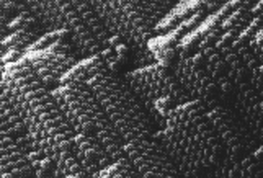
Electron micrograph of polystyrene beads close–packed in fcc structure.
The wavelengths of UV (ultraviolet), visible, and near infrared light range from about 200 through 2000 nm. When spherical beads uniformly sized in the 100–1000-nm range are arranged in periodic arrays and planes, with interplanar separations of tens to thousands of nm, such arrays will diffract light essentially identically as NaCl diffracts X-rays. This phenomenon occurs because the separations of periodic planes in such photonic band-gap materials are of the order of the wavelength of light. This periodicity leads, theoretically, to situations in which a photonic band gap material will allow light of certain wavelengths to pass but will block light of other wavelengths. Wavelength ranges that do not allow light to pass through the material represent optical or photonic band gaps, and provide a basis for designing light–based switching and amplifying devices [4,5]. Naturally occurring arrays of this type are known as opals (a class of semiprecious stones) [6], and light diffraction from opals produces iridescence.
1.1 Types of photonic crystals
There are two types of such photonic materials that we wish to discuss. The type illustrated in Fig. 1, wherein the beads are in physical contact with their nearest neighbors (12 nearest neighbors in the fcc structure illustrated), is the type of structure that offers the greatest number of degrees of freedom in producing new materials. For our purposes here we denote such systems as ‘contact’ photonic crystals, since nearest neighbors are in physical contact with each other. Another type of important photonic material is derived from crystalline arrays of charged particles, where nearest neighbors do not physically contact one another. These materials are known as colloidal crystalline arrays, CCA. This type of material also typically is manifested by beads adopting an fcc or bcc lattice structure. Such arrays of charged beads form under stringent conditions of low ionic strength in aqueous suspension. Charge repulsion between such beads induces crystallization.
1.2 Technological needs
Both types of crystalline materials have exhibited great promise for providing advanced materials for use in diverse applications. These ‘non-contact’ CCA lattices are a bit more limited in their application, because they have no solid modulus as made, and because they do not exhibit bicontinuity in their two constituent phases. The beads are a disperse phase and their environs compose a continuous phase. The continuous phase in such arrays must be chemically transformed into a solid, before such ‘crystals’ can be manipulated. However, the crystallization rate for CCA is relatively rapid in comparison to the rates of formation of ‘contact’ photonic crystals wherein nearest neighbors are touching one another [7]. Many laboratories are working on ways to make such arrays, but all of the methods so far disclosed rely on slow processes that produce only very few and very small crystals, suitable for research, but impractical for any conceivable manufacturing scenario. A need exists to provide a process for fabricating such materials that would be more suitable for manufacturing. We need to learn how to control supramolecular assembly. The best processes to date take tens of hours to produce and isolate single crystals suitable for only one device. If these kinds of materials are to ever have a significant technological impact, means must be found to make them in high yield.
2 Colloidal crystalline arrays
The formation of colloidal crystalline arrays (CCA) by latexes appears to have been discovered a bit over 30 years ago [8,9] and has since stimulated intense interest. While such arrays have been embraced as ideal model systems for studying crystal physics these CCA are exhibiting a wide variety of potentially useful properties for chemical sensing and for optical switching and tuning. Since monodisperse latexes can be fabricated over the sub-100-nm range into the micron range, wide variety exists in the optical properties and ranges of such materials. In addition, the nature of the polymer particles used can be varied from relatively ‘dense’ and cross–linked polystyrene (PS) to hydrogel particles that can thermoreversibly be transformed from identifiable particles to swollen particle shadows hardly distinguishable from a surrounding continuous phase.
One of the most profound properties of CCA is that they form at very low volume fractions in aqueous suspensions of low ionic strength. This property makes them ideal for crystallization studies.
2.1 Principles
The formation of fcc and bcc colloidal crystalline arrays, wherein the charged polymer beads do not touch one another, is more facile and less activated than the crystallization of beads in nearest neighbor contact, but suffers in that the resulting assemblies have elastic constants in the range of 10–100 erg cm–3, while atomic solids have elastic constants on the order of 1010 erg cm–3. In other words the arrays formed or crystallized from suspension have no significant solid modulus and are therefore unstable and subject to disordering by shaking, vibrations, etc. Handling such crystals without perturbing the optical characteristics is extremely difficult.
An aspect that facilitates such facile crystallization is that the particles are charged and so experience long-range electrostatic repulsion between one another long before coming into physical contact. This action at a distance serves to keep individual particle motion fairly unactivated so as to produce a crystalline array, typically fcc or bcc. An fcc structure is illustrated in Fig. 2 .

Illustration of fcc structures often adopted by charged particles in CCA. Here the particles have intrinsic negative charges with cationic counter ions (courtesy of Sandy Asher).
Detailed kinetic studies of such crystallization [10] have shown the crystallization is indeed facile at low volume fractions, and that the growth rates slow appreciably and nucleation rates increase dramatically on going from 0.004 to 0.04 in bead volume fraction.
While the crystalline structure of such CCA has generally been confirmed by Bragg diffraction of laser light and by direct visualization by optical microscopy, freeze fracture electron microscopy has successfully been applied to PS colloidal crystals [11]. This technique was shown to be invaluable in characterizing certain defects such as grain and twin boundaries, line dislocations, and point defects.
While one can imagine certain one–dimensional but tenuous applications for such an array [12], it is generally much more useful to convert the continuous (aqueous) phase into a solid phase. A particularly convenient way of doing this is to include a hydrogel monomer, such as acrylamide, in the aqueous phase and then polymerize the monomer to produce a solid hydrogel continuous phase of polyacrylamide. Such a solidification procedure produces a material that can then be handled without particularly disrupting the crystalline array within.
There have been few studies addressing size and charge polydispersity effects on crystallization in these systems. A simulation study [13] suggested that the charge polydispersity, CPD,
The need to generally use UV initiation to effect hydrogel polymerization in rigidifying CCA structures has been recently partially overcome by using PS particles that contain superparamagnetic iron oxide nanoparticles and a locally applied magnetic field gradient [14]. While the charged PS/iron oxide composite particles self assembled into CCA in deionized water, the packing was significantly affected by proximal magnetic field gradients. A magnetic field was found to induce interparticle magnetic moments that produced a repulsive force in the plane perpendicular to the magnetic field and an attractive force in the direction parallel to the field [15]. Such assembly usually cannot occur in high ionic strength conditions or in organic solvents because of ionic screening and the absence of interparticle long-range repulsion forces. This limitation can be overcome using a proximal magnet with such composite particles. In addition, the use of a proximal magnet facilitates UV initiation protocols that generate ionic species and that normally do not suffice when forming a hydrogel to rigidify the CCA without disrupting the long–range order.
2.2 Applications
Materials derived from these CCA have been applied in diverse ways. The first practical applications realized were in the production of narrow bandwidth filters. Such CCA are effectively one-dimensional band-gap materials and can be used as narrow bandwidth notch filters, such as indicated schematically in Fig. 3 . In the case a of Fig. 3, an incident beam 30 at θ1 largely is transmitted and emerges as 32, while a narrow band portion is diffracted as 34 due to the one-dimensional band gap illustrated in the lower part, curve A. Similarly, b illustrates the case where incident beam 40 impinges at θ3 < θ1, beam 42 emerges, and beam 44 at longer wavelength is diffracted at θ4. In this way narrow components may be selected from an incident beam by adjusting the controlling incident angle.
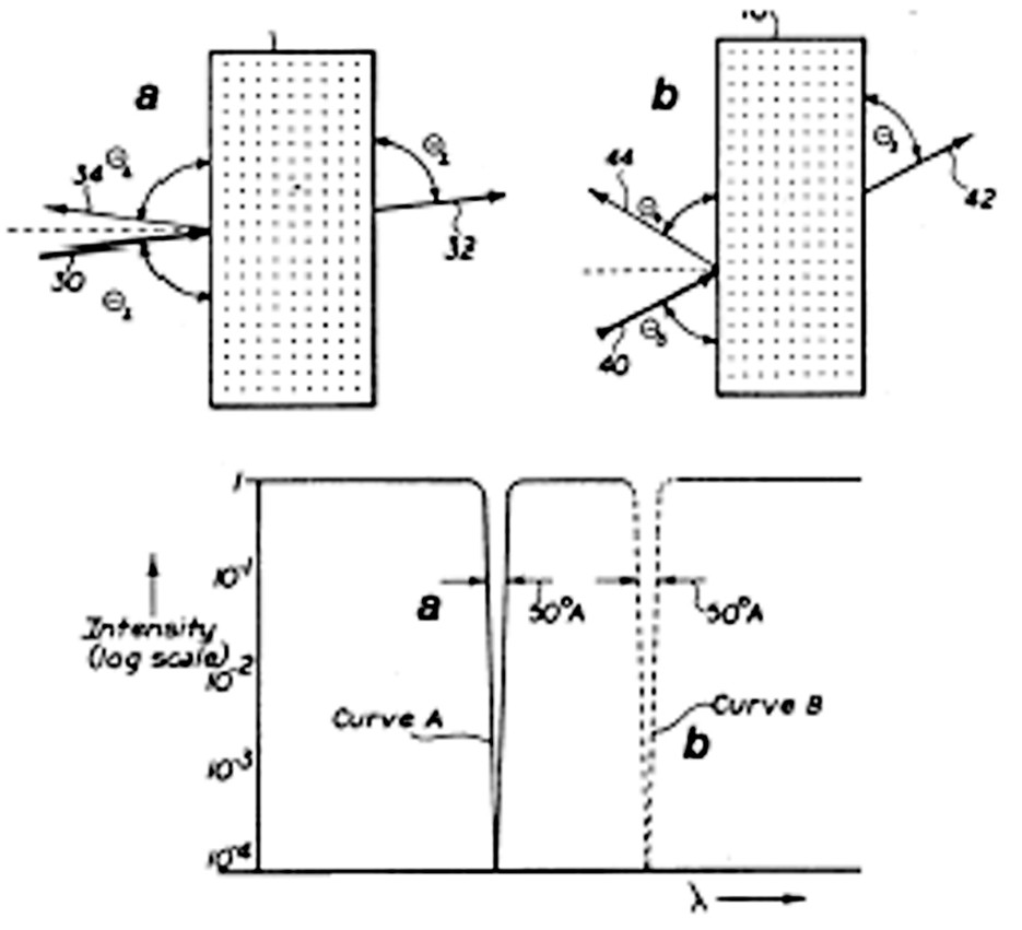
Narrow bandwidth radiation filter useful as a tunable beam splitter (adapted from [12]).
CCA have also been illustrated to provide thermally sensitive structures that can produce a variety of devices. CCA in a bcc structure composed of 100 nm particles [16] of poly(N-isoproplyacrylamide), PNIA, provide a very temperature sensitive probe. Since PNIA has thermoreversible properties, particles in the CCA contract when the temperature is raised from 24 to 35 °C. This contraction results in a denser particle with a different refractive index, and the narrow bandwidth extinction at about 530 nm increases 5-fold in magnitude.
In a related system [17], PS beads (99 nm) were used to form a CCA in a bcc lattice and a thermally reversible hydrogel, PNIA, was polymerized in the continuous phase to lock-in the structure. In this material the overall lattice constant changes with temperature, and the peak extinction wavelength shifts from 450 nm to 700 nm as temperature shifts from 35 to 10 °C.
Relatively fast optical switching has been obtained [16,18] using 138 nm latexes of heptafluorobutyl methacrylate with Oil Blue N dye encapsulated during the emulsion polymerization. The bcc CCA structure was locked in by copolymerizing acrylamide and N,N-methylene bisacrylamide, to provide a cross–linked continuous phase. Nanosecond optical switching was obtained using a 594-nm probe laser beam and a 532-nm pump laser. The 800-μm thick CCA was oriented to satisfy the Bragg condition for the probe beam. The index of refraction of the CCA was adjusted with DMSO (n = 1.479) so that the continuous phase index matched the particle index (n = 1.386). These dyed particles heat under irradiation, and the particle refractive index then decreases. With the CCA in a medium adjusted to n = 1.3908, pump heating of the particles decreases the particle refractive index from 1.386 and the magnitude of diffraction increases. With the medium adjusted to n = 1.3813, pump heating decreases the particle refraction and the diffraction decreases.
Nanosecond switching has been demonstrated in a similar device [19], using an fcc CCA of PMMA beads (n = 1.492) dyed using a photoabsorbing and nonfluorescent dye (so absorbed energy is channeled into heating). The continuous phase was index matched using water (n = 1.336) and methylphenylsulfoxide (n = 1.57). The incident 10 mW cm–2 450-nm laser beam impinging on a 50-μm-thick dyed and index-matched CCA at normal incidence was attenuated with a decay time of about 2.3 ns.
Significant mention must also be made of the high potential for CCA materials as chemical sensors [15]. Chemically sensitive ligands, enzymes, etc. may be attached to particles used in CCA as well as to the hydrogel polymers used to provide a solid modulus in such materials. Depending on the particular kind of chemical analyte–receptor interaction, various effects are achieved in modifying the lattice constant of the CCA and the ensuing apparent absorption band. Such sensors probing pH and ionic strength have recently been detailed [20].
A switch sensitive to a particular metal cation causes a change in the ionic environment [21] upon complexation of the cation. This electrostatic change perturbs the Donnan equilibria, and osmotic forces drive differential swelling, thereby changing the crystalline lattice constant. This structural change results in a color change that can be detected quantitatively very cheaply. The structure and operation of such optical switches is illustrated in Fig. 4 , where a monomer incorporating a crown ether type of ligand was included in the hydrogel polymerization process. Pb2+ binding to the crown ether results in significantly increased electrostatic repulsion in the hydrogel, and the lattice constant increases and is tracked by shifts in the visible absorption peak maximum. Similar devices probing other analytes have been produced, including a glucose sensor [22] that was successfully implanted into a rabbit ear to provide in situ reflectance monitoring of blood glucose levels [23].
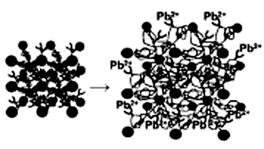
Chemical sensor based on hydrogel-stabilized crystalline colloidal array (courtesy of Sandy Asher).
3 ‘Contact’ photonic crystals
The iridescence of opals has long been known, but it has been only within the last forty years that the basis for these optical effects was revealed as coming from light diffraction from amorphous silica spheres arranged in various crystalline lattices. The mechanism of formation of these crystalline arrays is not known, but crystals of single monodisperse spheres as well as crystals of bidisperse [6] spheres have been identified in natural opals. The silicate spheres in these opals are amorphous. Their long-range crystalline ordering and their sizes in the wavelength ranges close to those of visible light result in diffraction of light in complete analogy to the Bragg diffraction of X-rays from ordered atoms in atomic and molecular crystals.
3.1 Motivation
The great promise offered by such ‘contact’ photonic crystals derives from their bicontinuous structure. Since the beads are in nearest neighbor contact they form a continuous phase spanning the material. In addition, the interstices are all simply connected and compose a separate continuous-phase domain. Because of this bicontinuity, various chemical sequences may be employed to synthesize various materials, as illustrated in Fig. 5 .

Templating close-packed photonic arrays. The interstices of a close-packed array may be filled with almost any organic or inorganic phase to produce an opal-like composite. The beads may often be removed by dissolution or by pyrolysis to produce a porous replica (courtesy of O. Velev).
The starting colloidal crystal may be transformed into an opal-like composite by filling the interstices with another phase. Examples now exist illustrating such filling with diverse types of organic and inorganic phases. Subsequently, additional chemical (e.g., etching or dissolution) or physical (e.g., calcining) steps may be invoked to remove the bead-based ‘internal’ phase, leaving a negative image of it in the newly formed exterior or interstitial phase. This negative image, since it is continuous, may then be filled with another chemical phase if desired. In any case, these introductory examples illustrate that diverse classes of materials may be derived from photonic crystals via various templating chemistries (discussed below).
The quest for photonic band-gap materials that block light transmission in all directions is very active, as such materials will provide a basis for light processing in analogy to the above-mentioned electron processing by semiconductors. A recent report details the preparation of photonic crystals composed of anisotropically shaped (egg shaped) colloidal inorganic particles [24]. We expect it will not be too long before similar preparations are achieved using shape anisotropic polymer colloids. Anisotropic shapes promote setting the stage for physically tuning various photonic properties.
3.2 Difficulties
A significant difficulty with such ‘contact’ crystals is that they take a long time to make, and the crystals made are not very big. To understand the practical aspects of this difficulty, keep in mind that fcc crystals of monodisperse beads occupy 74% of space. A liquid-to-solid (glass) transition occurs in such monodisperse systems at a volume fraction of about 0.49–0.50. Hence it is easy to see how transformation from a volume fraction of 0.5 to a volume fraction of 0.74 will in general be a highly activated process.
3.3 Synthesis methods
Early synthetic approaches were serendipitous and resulted from sedimentation in a gravitational field. Iridescent layers in latex suspensions were noticed after lengthy settling, and then subsequently analyzed to identify a colloidal crystalline phase. This approach is inexpensive but highly time consuming.
Some successes have been registered by using sedimentation in a centrifugal field, but this approach is not a method of choice. A recent [25] and very interesting application of centrifugation is in the use of thermoreversible particles to produce close packed photonic crystals that are thermoresponsive and provide variations in optical properties reminiscent of the thermoreversible effects discussed above for CCA materials. In this approach, 210 nm hydrogel particles are synthesized as copolymers of N-isopropyl acrylamide (NIPAM) and acrylic acid (AA) with about 2 mol% crosslinker, N,N′-methylenebisacrylamide. In the low temperature (unswollen) state a suspension of these particles is centrifuged and an iridescent layer is recovered at the bottom of the centrifuge tube. Upper layers are decanted, and this iridescent layer can be cycled between a photonic crystalline state (of iridescence) and a liquid milky state that is free flowing. Cycling results in reversible ordering into the photonic crystalline state. Such materials may hold great promise for rapid and large-scale production of photonic crystals, but the initially required centrifugation step will have to be overcome.
Evaporation of monodisperse latex beads at an early stage revealed the production of both hexagonal and square arrays and suggested such thin arrays could be used as diffraction gratings [26]. A recent, very small scale, evaporation study reported the production of thin photonic crystals, with domain sizes ranging from 50 to 300 μm [27]. The use of core-shell latexes has been claimed to provide easy self-assembly into photonic crystals by evaporation, but domain sizes are small and one must search among many fragments for single crystals [28]. Another twist to the evaporation approach is to generate large aerosol droplets of dense suspensions of monodisperse beads. As evaporation is driven, in for example a spray tower, the beads condense and crystallize, and form photonic supraspheres [29].
An osmotic pressure thermal gradient approach operating in the liquid–solid volume fraction range of 0.48–0.55 has succeeded in producing random hexagonal close packed (rhcp) crystals with largest dimensions of about 3 mm in about 2 weeks time [30].
Various electrophoretic and electrodeposition techniques have been reported, but such approaches remain laboratory curiosities. Very interesting entropic approaches, also using surface templating, have succeeded in yielding modestly thick (30–50 layers) crystals [31]. A mica surface templating approach using simple drying has recently been reported as facile [32]. However, details on thickness and single domain boundary lengths were omitted.
The most accomplished method to date appears to be a hybrid process developed in Xia’s laboratory [5]. This approach combines filtration and sonication or vibration, in order to produce finite results in 24 h. A schematic of the approach is illustrated in Fig. 6 . The exit channels are controlled so that beads cannot flow out. The aqueous dispersion of beads is semicontinuously fed into the chamber, and the whole assembly is mounted on a vibrator, thereby providing activation to drive crystal formation. Beads small enough to flow through the exit channels can be processed successfully in such a device, by simply using several layers of larger beads to block access to the exit channels prior to introducing the smaller beads.

Thin colloidal crystals formed using commensurate filtration (courtesy of Younan Xia).
3.4 Templates for other materials
The basic templating approaches are nicely summarized in Fig. 5. The devil is in the details, but there is great latitude available. Although high ‘band-gap’ quality demands considerable crystallinity, many applications derived from templating work very well with crystals containing many defects and with arrays that result essentially from random packing.
The creation of nanoporous or mesoporous metal oxides of high surface area, such as illustrated in the bottom right of Fig. 5 can be simply obtained using very well established sol–gel chemistry [33]. An alcoholic solution of metal alkoxide (e.g., tetraethoxy silane) is allowed to permeate the colloidal crystal and catalytic water is added along with heating. The metal alkoxide converts to amorphous metal oxide, and further heating such as calcinations at 575 °C, pyrolyzes away the polymer beads and leaves a high surface area mesoporous film as a negative image of the colloidal crystal.
Another approach to producing metal oxides is to precipitate a metal oxalate, e.g. nickel oxalate, and then to convert to oxide by heating and decarboxylation [34].
The production of metal frameworks can be accomplished by several different routes. For example, the NiO framework just discussed can be converted to high surface area nickel by simple reduction in an activated hydrogen atmosphere. Similar approaches have been used to produce a reverse phase of GeO2 from tetramethyl germane, followed by reduction of the GeO2 to Ge in inverse opal form [35]. Alternatively, the nickel oxalate can be directly converted to the metal by anaerobic heating and decarboxylation [36]. Noble metal frameworks may be simply constructed by filling the interstices with suspensions of noble metal nanoparticles (e.g., gold). Drying and sintering provides nanoparticle–nanoparticle cohesion as well as removal of the templating polymer beads.
Composite materials such as the opal-like composite or the structured porous replica pictured in Fig. 5 can easily be produced by perfusing with liquid polymer or polymer precursor. Polystyrene (PS) templates have been converted to very uniform polyurethane membranes by curing a urethane solution in situ and following with dissolution of the PS beads using toluene. Similarly, colloidal crystals can be formed from monodisperse core–shell polymer colloids. With the proviso that the shell is sufficiently thick, and has a Tg lower than that of the core polymer, annealing transforms a particle assembly into a polymer bloc composite such as pictured in the middle right of Fig. 5 [36].
An electrochemical approach to producing an inverse opal structure from PS colloidal crystals has been reported [37]. The colloidal crystal is placed on a conducting electrode, such as an ITO (indium tin oxide) electrode and inside an electrochemical cell containing an acidic solution of CdSO4 and SeO2; a Pt anode; an SCE reference electrode. Galvanostatic or potentiostatic precipitation of CdSe is followed by toluene dissolution of the PS template particles.
The types of chemistries that can be used to perfuse and fill the interstices have quite recently been reviewed [38,39]. Simple and ternary oxides, chalcongenides, non-metallic and metallic elements, carbon allotropes, hybrid organo-silicates and polymers can be obtained. The techniques used to produce such phases include, in addition to sol–gel chemistry, polymerization, salt precipitation, chemical conversion, chemical vapor deposition, spray pyrolysis, ion spraying, laser spraying, nanocrystal deposition and sintering, oxide and salt reduction, electrodeposition, electroless deposition, fabrication from core-shell spheres, and patterning methods.
4 Summary
New and exciting applications of CCA will involve using electrostatic ordering to create crystals of monodisperse colloids in which the colloids themselves (silver halide microcrystals, dye crystallites, amorphous dye particles, and semiconductor particles) manifest the chief property of interest (light sensitivity, conductivity, light extinction). For example, dispersing silver halides in a regular array would allow imaging with a minimum of granularity (noise), compared with extant imaging systems in which silver halide is placed randomly in a given layer. Lattice constants may be controlled with ionic strength and through the surface charge on the nanoparticulates. Such arrays will provide novel optical-switching materials. The development of full and partial photon band-gap materials has been intensely focused upon in the past several years. Recently, a photon (full) band-gap device operating in the visible has been reported [5], and extensions to other wavelengths and a plethora of self-assembled systems are being pursued by many groups.