

1 General introduction
Considerable effort has been recently devoted to the preparation of thin films of organic-based materials [1]. The main techniques used for their preparation are Langmuir–Blodgett, high vacuum evaporation, electrochemical deposition, molecular beam deposition, and chemical vapor deposition (CVD) methods. However, thin films of organometallic- or metalorganic-based materials remain relatively rare. For instance, Prussian blue and Prussian blue-like magnetic materials have been processed as thin films by using either electrodeposition [2–4] or Langmuir–Blodgett [5] techniques. These two methods have also shown their efficiency for growing thin conducting films of bis(dithiolene) complexes [6–8].
In this paper, our goal is to study the processing of metal complexes-based molecular materials on silicon wafers, substrate of choice for electronic applications. We will illustrate the use of intrinsic silicon (001) wafers in two different processing techniques, i.e. CVD, and electrodeposition. CVD will be applied to prepare thin films of molecule-based magnets of the M(TCNE)x family (M: V, Cr, Nb, Mo; TCNE: tetracyanoethylene (NC)2C=C(CN)2). Moreover, the electrodeposition technique will be used for processing conducting deposits of [(n-C4H9)4N]2[Ni(dcbdt)2]5 (dcbdt2–: 4,5-dicyanobenzene-1,2-dithiolato, Scheme 1) and TTF[Ni(dmit)2]2 (TTF: tetrathiafulvalene, Scheme 2; dmit2–: 1,3-dithiole-2-thione-4,5-dithiolato, Scheme 3).
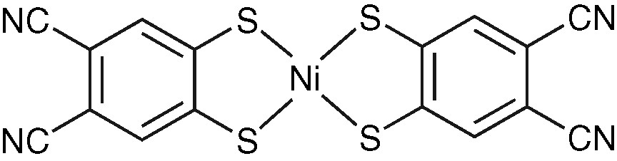
Molecular structure of Ni(dcbdt)2.
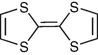
Molecular structure of TTF.
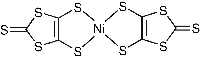
Molecular structure of Ni(dmit)2.
2 Experimental
2.1 Substrates and starting compounds
Intrinsic Si(001) wafers (one face polished) are purchased from Siltronix (diameter: 5 cm; thickness: 275 μm; conductivity at room temperature ~10–3 S cm–1). The wafers are striped in a NH4F/HF solution (12.5% HF at 50% and 87.5% NH4F at 40%) and then washed in distilled water before use. TCNE is purchased from Aldrich and freshly sublimed before use. Bis(benzene) vanadium, V(C6H6)2, is purchased from Stream Chemicals and bis(benzene) chromium, Cr(C6H6)2, is prepared following a previously described procedure [9]. Tris(1,4-diisopropyl-1,4-diazabuta-1,3-diene)niobium, Nb(iPr2-dad)3 [10], and bis(mesitylene)niobium, Nb(mes)2 [11], are prepared according to the literature data. Bis(toluene)molybdenum, Mo(C6H5CH3)2, was prepared following a previously described procedure [12]. TTF was purchased from Sigma and used without further purification. [(n-C4H9)4N][Ni(dmit)2] was synthesized according to Ref. [13]. Finally, [(n-C4H9)4N][Ni(dcbdt)2] [14] was supplied by Dr. M. Almeida (Departamento de Química, Instituto Tecnológico Nuclear, Sacavém, Portugal).
2.2 CVD procedure
Thin films of M(TCNE)x are deposited from TCNE and the metal complex (Table 1), using a conventional hot-wall CVD apparatus [15]. The glass crucibles are charged with the starting compounds inside an argon-filled glove box. The intrinsic Si(001) wafers (1 cm × 1 cm) are placed on top of a glass slide inside the reactor and the CVD system is then pumped for 15 h down to ~10–3 Pa, while the carrier lines are heated at 353 K and the reactor at 423 K. The precursors are vaporized at 200 Pa, and transported by helium carrier gas to the mixing zone (448 K) and then to the deposition zone. The mixing zone is held at 448 K in order to avoid condensation of the starting compounds. After their preparation, the films are removed from the deposition zone under an argon flow and finally stored in an argon-filled glove box.
Experimental CVD conditions for film formation of M(TCNE)x
| Precursor mass (mg) | Vaporization temperature (K) | Helium flow rate (cm3 min–1) | Substrate zone temperature (K) | Deposition duration (min) |
| V(C6H6)2: 150 | 418 | 28 | ||
| 313 (a) | 180 | |||
| TCNE: 180 | 356 | 10 | ||
| Cr(C6H6)2: 145 | 423 | 17 | ||
| 353 (b) | 90 | |||
| TCNE: 190 | 356 | 10 | ||
| Nb(iPr2-dad)3: 110 | 418 | 17 | ||
| 353 | 180 | |||
| TCNE: 110 | 356 | 10 | ||
| Mo(C6H5CH3)2: 220 | 388 | 10 | ||
| 373 | 40 | |||
| TCNE: 240 | 356 | 10 |
2.3 Electrodeposition procedure
Electrodeposition of TTF[Ni(dmit)2]2 is carried out in a H-shaped electrochemical cell (24 ml) with intrinsic Si(001) as anode (0.5 cm × 1 cm) and a platinum wire as cathode (solvent: freshly distilled and degassed acetonitrile). We have selected silicon single crystals (vs. polycrystalline silicon) as substrates in order to eliminate spurious effects associated to grain boundaries, avoiding e.g. non-homogeneous current densities. The anodic oxidation of the TTF is performed at constant current density at room temperature (Table 2). Within 5 days, a black air-stable thin film is mainly formed on the non-polished face of the (001)-oriented silicon electrode. On the polished face, only a small amount of material is observed but is found to be easily unsticked from the surface due to small mechanical stresses.
Experimental conditions for film formation of TTF[Ni(dmit)2]2
| Anodic compartment | Cathodic compartment | ||
| TTF (mol) | [(n-C4H9)4N][Ni(dmit)2] (mol) | [(n-C4H9)4N][Ni(dmit)2] (mol) | j (μA cm–2) |
| 3.9 × 10⁻⁵ | 1.3 × 10⁻⁵ | 1.3 × 10⁻⁵ | 1.5 |
| 6.0 × 10⁻⁵ | 1.0 × 10⁻⁵ | 7.0 × 10⁻⁵ | 0.8 |
| 6.0 × 10⁻⁵ | 1.0 × 10⁻⁵ | 7.0 × 10⁻⁵ | 1.5 |
| 6.0 × 10⁻⁵ | 1.0 × 10⁻⁵ | 7.0 × 10⁻⁵ | 2.5 |
Electrodeposition of [(n-C4H9)4N]2[Ni(dcbdt)2]5 is carried out on an entire silicon wafer (diameter: 5 cm). A solution of [(n-C4H9)4N][Ni(dcbdt)2] (110 mg) in freshly distilled and degassed CH2Cl2 (230 ml) is introduced into a Schlenk-type cylindrical one-compartment electrochemical cell (400 ml). The galvanostatic oxidation (0.5 μA cm–2) is performed at 298 K. Within a day, black microcrystals appear and grow homogeneously on the Si surface. A ~10 μm continuous, adherent and air-stable thin film is obtained after a 4 days electrolysis duration.
2.4 Characterization methods
Scanning electron micrographs (SEM) are obtained on a JEOL Model JSM 840A microscope. Infrared spectra are recorded using a Perkin–Elmer Spectrum GX spectrophotometer. The Raman measurements are performed using a DILOR XY micro-Raman set-up. The spectra are obtained at room temperature using the 647 nm line of a Kr laser. The incident beam is focused onto the film through the × 100 microscope objective, giving a spot size of ~1 μm2. The back-scattered light is collected through the same objective, dispersed and then imaged onto a CCD detector. Using a laser power density of about 105 W cm–2, no major degradation of the material appears. X-ray diffraction data are collected with a Seifert XRD 3000 TT, using the Cu Kα radiation (1.5418 Å), fitted with a diffracted beam monochromator. The diffractometer is in Bragg–Brentano configuration (θ/θ). XPS spectra of magnetic thin films are recorded using a VG Escalab Model MK2 spectrophotometer, working with monochromatic Mg Kα radiation (1253.6 eV). X-ray photoelectron spectra of conducting thin films are acquired with an EA10P hemispherical analyzer (SPECS) using non-monochromatized Al Kα radiation (1486.6 eV). X-ray absorption spectra of Cr(TCNE)x deposits are performed on the XAS 13 beam line at the French synchrotron facility DCI at LURE (Orsay). Spectra are recorded at the chromium K-edge in transmission mode using Si 311 (X-ray absorption near edge structure, XANES) and Si 111 (extended X-ray absorption fine structure, EXAFS) double monochromator detuned around 30% to ensure harmonic rejection. The edge energy of the chromium (5989 eV) is fixed at the first inflexion point of a chromium foil. Magnetic data are taken on a MPMS 5.5 Quantum Design SQUID magnetometer. Conductivity measurements are performed using the standard four-probe method. Electrical contacts between the gold wires and the film are made by using gold paint. They are drawn parallel to each other keeping a large inter-wire distance (~2.2 mm).
3 Results and discussion
3.1 M(TCNE)x magnets as thin films
3.1.1 Introduction
Recently, the study of molecule-based magnets exhibiting spontaneous magnetization at room temperature has attracted increasing interest [16,17]. These light weight materials, obtained from an organometallic route, represent an interesting alternative to conventional magnets in future generations of devices. M(TCNE)x, y solvent (x ~ 2; 0.5 ≤ y ≤ 2; M: first-row transition metal, namely, V, Mn, Fe, Co, Ni) are molecule-based ferrimagnets with critical temperatures ranging from 45 to 400 K and coercive fields as great as 6.5 kOe [18]. We have recently reported the preparation of M(TCNE)x (M: V, Cr) magnets as thin films on alkali halide substrates using CVD [19,20]. However, alkali halides are not the most appropriate for potential applications. Moreover, deposits obtained on alkali halides were found to be easily unsticked due to small mechanical stresses. On the other hand, it is to be noticed that M(TCNE)x, y solvent systems are not known with second-row transition metals. In the following 3.1.2 and 3.1.3 paragraphs, we describe the use of CVD to the formation of solvent free-M(TCNE)x (M: V, Cr, Nb, Mo) molecular magnets on silicon, this latter constituting a more suitable substrate for potential applications.
3.1.2 Vanadium and chromium-based magnets
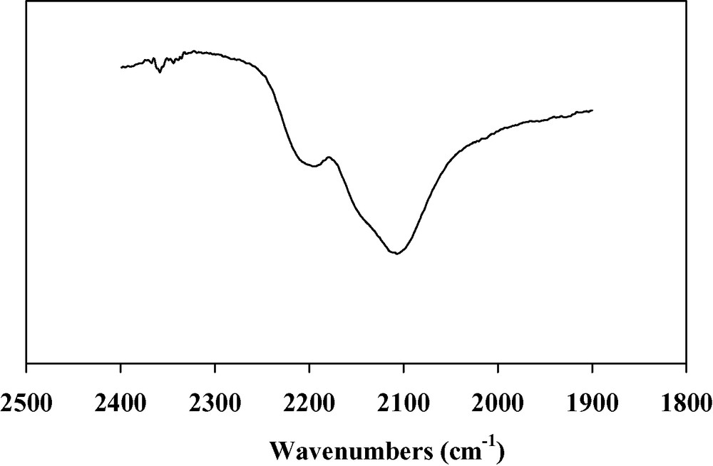
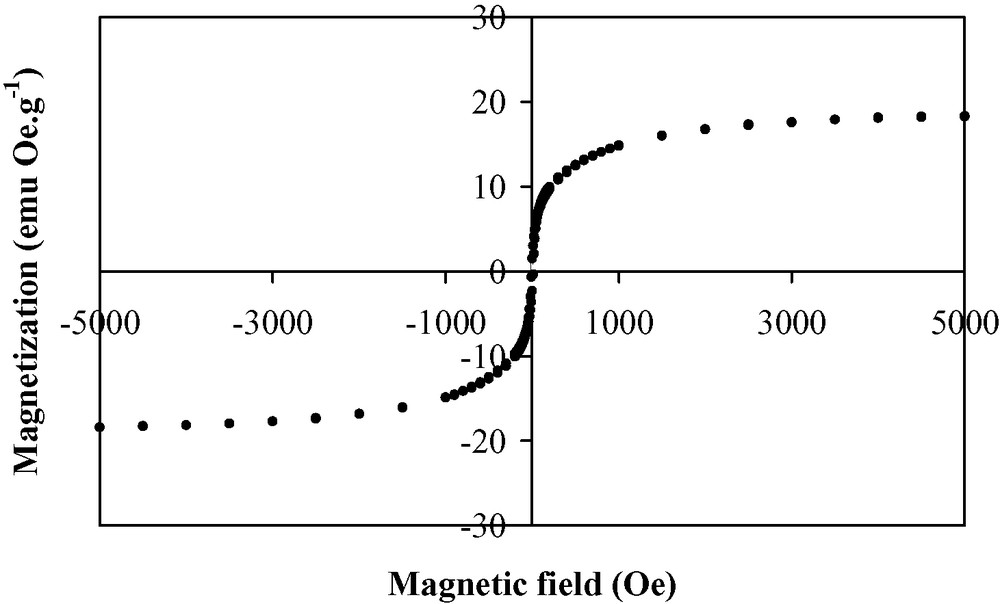
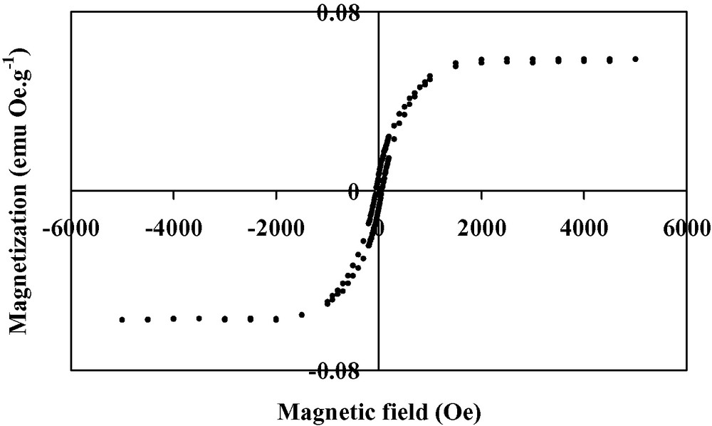
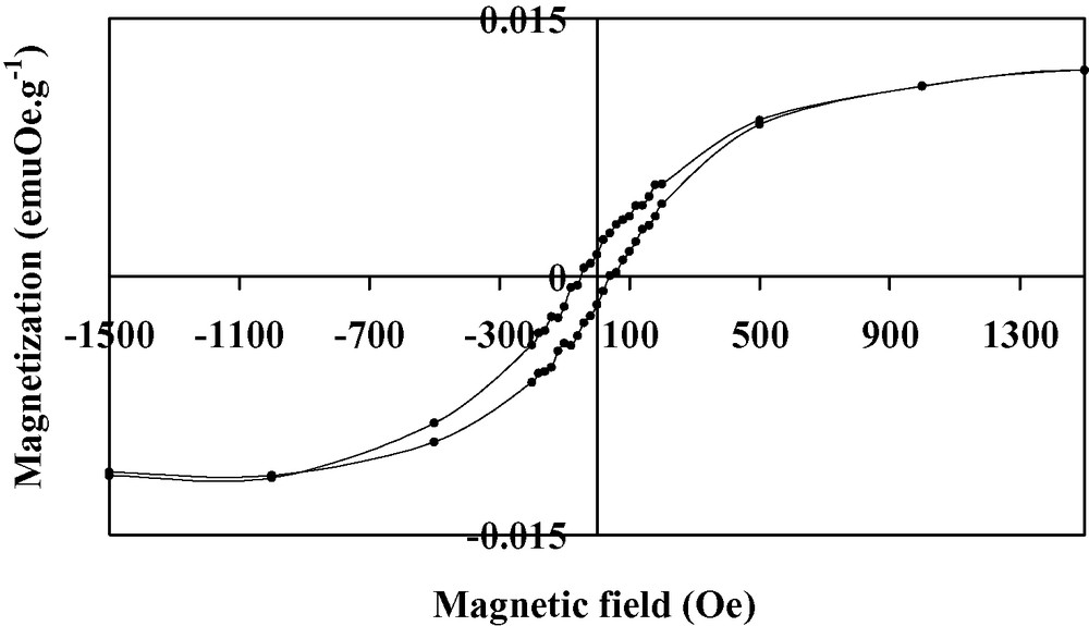
Thin films of the V(TCNE)x phase are deposited on silicon substrates from V(C6H6)2 and TCNE, in the conditions reported in Table 1. The loss of the benzene rings occurs at a relatively low temperature (313 K). The black deposits thus obtained have an amorphous character. The films do not spontaneously peel off (contrary to what observed on alkali halides). However, the deposits are very sensitive towards air exposure. To improve their stability (~1 h), they are further annealed at 343 K for 10 h under a helium atmosphere. After the thermal treatment, the amorphous character of the films is maintained. SEM images of annealed films evidence roughly spherical sub-micrometer grains (Fig. 1). The infrared spectra show no νCH bands corresponding to the presence of the aromatic ligands, thus confirming the loss of the benzene rings. Furthermore, two broad νCN bands are observed at 2106(s) and 2195(m) cm–1 (Fig. 2), consistent with a monoreduced TCNE moiety (TCNE•–) bound to four vanadium atoms via σ-N bonds [18]. A shoulder at 2145 cm–1 is also observed and may be assigned to TCNE•– trans-μ-bound to two vanadiums [21]. X-ray photoelectron data evidence the presence of V, C, N and O. The presence of oxygen (<1 at.%) is due to surface contamination. The N1s peak is at 397.7 eV, in agreement with monoreduced TCNE, i.e. TCNE•– [22]. The V2p3/2 line has a binding energy at 513.3 eV, a typical value for VII [23]. The magnetization measurements at 5 K for the annealed films reveal a saturation magnetization of ~0.5 emuOe g–1. This value is lower than that observed for as-deposited V(TCNE)x films (~18 emuOe g–1, Fig. 3). J.S. Miller et al. also reported that thermal treatment of solution grown V(TCNE)2·0.5CH2Cl2 reduced the magnetization values [18]. It is to be remarked that as-deposited V(TCNE)x shows only two broad νCN absorptions at 2105(s) and 2192(m) cm–1, attributable to TCNE•– bound to four vanadiums [19]. For the annealed films, some TCNE•–s seems to be trans-μ-bound to two vanadiums (further absorption at 2145 cm–1). This partial decoordination from the VII centers would block some spin-coupling pathways and could induce magnetic disorder. However, after thermal treatment, a spontaneous magnetization remains at room temperature as shown on Fig. 4. The hysteresis loop (magnetization vs. applied magnetic field) evidences a coercive field of ~50 Oe and a saturation induction of ~2.5 kOe, to be compared to ~80 Oe and ~0.8 kOe for as-deposited V(TCNE)x [19]. Furthermore, after thermal treatment and air exposure (Fig. 5), a hysteresis loop is still observed at room temperature (coercive field ~50 Oe and saturation magnetization ~1.2 × 10⁻² emuOe g–1, to be compared to ~50 Oe and ~5.9 × 10⁻² emuOe g–1 for annealed samples without air exposure).
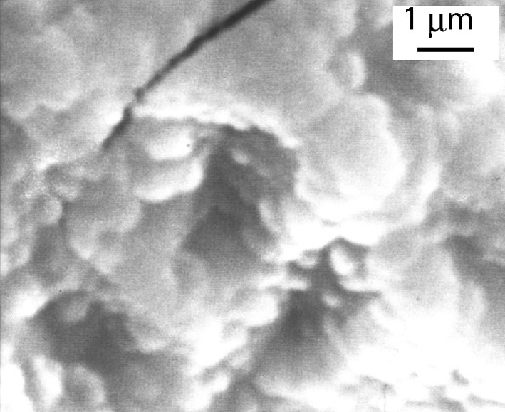
SEM image of annealed V(TCNE)x thin films.
IR spectrum of annealed V(TCNE)x thin films (νCN region).
Hysteresis loop at 5 K for as-deposited V(TCNE)x thin films.
Hysteresis loop at 300 K for annealed V(TCNE)x thin films.
Hysteresis loop at 300 K for annealed V(TCNE)x thin films after air exposure.
Black amorphous thin films of Cr(TCNE)x are prepared on silicon substrates via CVD of Cr(C6H6)2 and TCNE precursors (Table 1). The loss of the benzene rings is achieved when operating at 353 K and further annealing the deposits at 373 K for 2 h under a helium flow. As observed for the vanadium-based deposits, Cr(TCNE)x as thin films do not spontaneously peel off from the silicon surface. The films can be handled in air for ~5 h. SEM micrographs evidence a uniform film in which numerous cracks are clearly observed (Fig. 6). However, their presence does not affect too much the adherence of the films onto the Si surface. The infrared spectra show two broad νCN bands at 2116(s) and 2202(m) cm–1, consistent with TCNE•– ligands coordinated as μn-N-σ to the metal (n = 2–4) [16]. The Cr2p3/2 line has a binding energy at 576.3 eV, a typical value for CrII organometallic complexes, such as Cr(C5H5)2 [24]. The chromium K-edge spectrum (XANES) of Cr(TCNE)x is shown on Fig. 7. Its overall feature is in agreement with that of octahedral [ML6]2+ complexes (M = VII to CuII) [25]. The top of the edge energy is 6009 eV (C), close to that for low-oxidation state chromium (CrII or CrIII). The D signal is due to multiple scattering [25]. The spectrum also displays two peaks of weak intensity at 5992 eV (A) and 5996 eV (B). Signal A is assigned to 1s to 3d transitions, forbidden in regular octahedral complexes, but partially allowed in irregular ones [26]. The presence of this peak evidences an irregular octahedral environment for the chromium atoms within the deposit. Signal B is assigned to an allowed transition from 1s to a molecular orbital combining p orbitals of the chromium and π*CN [26], thus confirming the presence of coordinated TCNE•–. At the chromium K-edge, the Fourier transform of the EXAFS signal displays two peaks assigned to two shells around the chromium (Fig. 8). They correspond to the nitrogen and carbon atoms of the TCNE ligand. To extract information about the distances and the bond angles around the metallic atoms, we model the EXAFS signal using the FEFF7 code [27]. The structural parameters that fit best with the experimental data are the following: six nitrogen neighbors around chromium, a mean Cr–N distance of 2.03 Å, a N–C distance of 1.30 Å and a 160° Cr–N–C angle. It is to be remarked that the Cr–N distance in cyanato (–N=C=O), thiocyanato (–N=C=S) and alkylidineamido (–N=CRR′) CrIII-complexes are in the range 1.95–1.99 Å [28]. In our case, a larger Cr–N distance suggests a lower oxidation state, i.e. CrII, thus confirming XPS results. The 2–300 K magnetic susceptibility of the films can be fit to the Curie–Weiss law above 80 K with a θ value of –95 K (Fig. 9). Consequently, the magnetic interaction between the spin centers is strongly antiferromagnetic. At 2.5 K, the magnetization value for an applied field of 65 kOe is ~11 emuOe g–1 (Fig. 10). Inset in Fig. 10 shows the hysteresis loop recorded in the low-field region at 2.5 K (coercive field ~100 Oe). It clearly evidences that the films exhibit spontaneous magnetization at this temperature, whilst the corresponding Cr(TCNE)x·y solvent are not magnetically ordered above 2 K, presumably due to the deleterious effect of the solvent molecules [29].
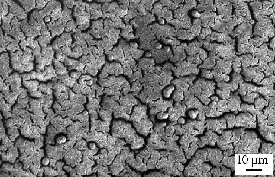
SEM image of Cr(TCNE)x thin films.

XANES chromium K-edge spectrum of Cr(TCNE)x thin films.
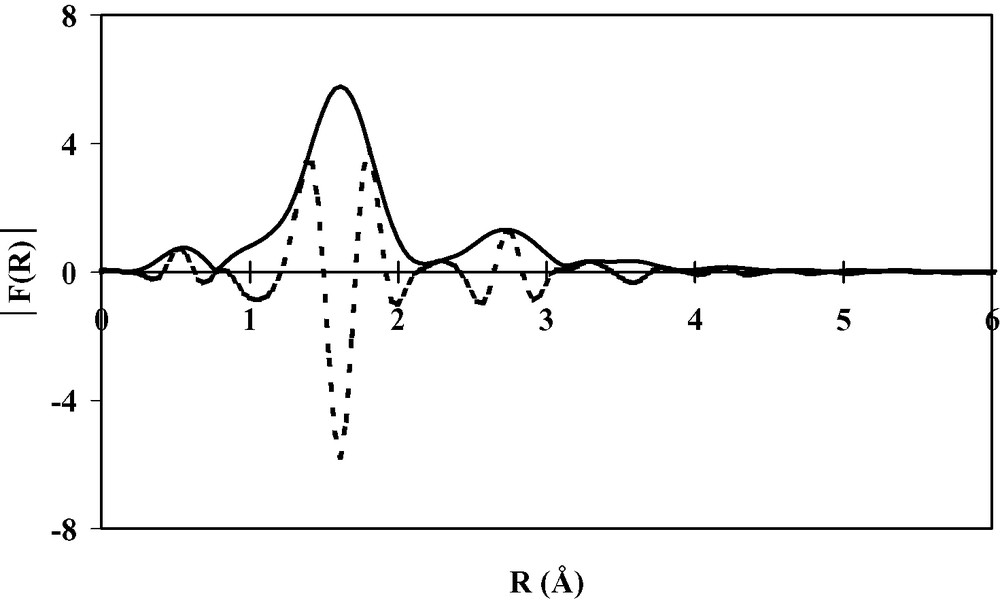
Fourier transform modulus ∣F(R)∣ (solid line) and imaginary part (dotted line) of the EXAFS signal at the chromium K-edge.

Reciprocal magnetic susceptibility vs. temperature for Cr(TCNE)x thin films.

Hysteresis loop at 2.5 K for Cr(TCNE)x thin films.
3.1.3 Niobium and molybdenum-based magnets
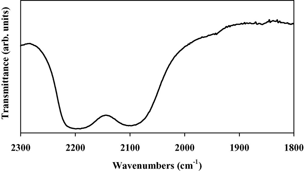
Black amorphous thin films of Nb(TCNE)x are grown from the gas phase reaction of Nb(iPr2-dad)3 and TCNE. They are air sensitive but relatively adherent on Si(001) wafers. The infrared spectrum of the films exhibits three bands at 2200(s), 2180(sh), and 2102(s) cm–1 (Fig. 11). They are in agreement with the presence of reduced TCNE moieties bound to Nb. The N1s X-ray photoelectron spectrum has two components at 398.1 and 399.9 eV, respectively, assigned to nitrogen atoms in TCNE•– bound to Nb and to nitrogen atoms in TCNE0, the oxidation product of TCNE•– [22]. XPS analyses also evidence that the Nb3d5/2 and Nb3d3/2 lines are split into two components at 204.4, 206.3, 207.2, and 209.2 eV. The 204.4 and 207.2 peaks (60%) are attributed to NbII by comparison with XPS data related to Nb2+ ions implanted into sapphire [30]. The other peaks (40%) correspond to NbO2 [31], whose presence is assigned to surface oxidation caused by handling the samples in the air before XPS measurements. After a bombardment of the films by Ar+ ions for 15 min. which allows the removal of the surface oxide, the XPS spectrum shows then clearly two peaks (6:4) corresponding to the 3d5/2 (204.6 eV) and 3d3/2 (207.4 eV) levels of NbII. SEM images evidence a film uniformly covering the substrate surface (Fig. 12). Some defects occasionally encountered allow us to evaluate the thickness of the film at ~3 μm. Magnetic measurements evidence that the films exhibit a spontaneous magnetization at 2.5 K. Fig. 13 shows the first and the second magnetization curves at this temperature. They evidence a saturation induction of ~20 kOe and a coercive field of ~200 Oe.
IR spectrum of Nb(TCNE)x thin films (νCN region).
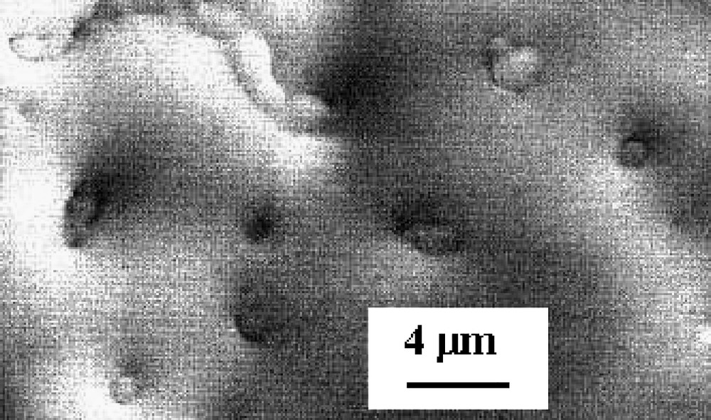
SEM image of Nb(TCNE)x thin films.
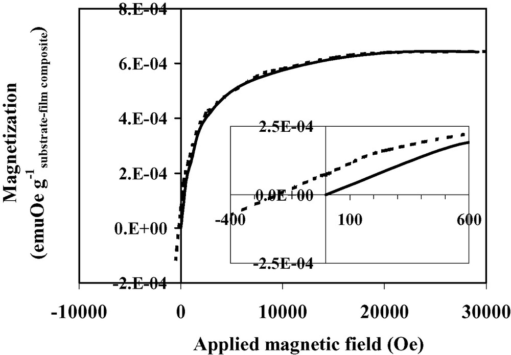
Magnetization vs. applied magnetic field for Nb(TCNE)x thin films at 2.5 K (first magnetization: solid line, second magnetization: dotted line).
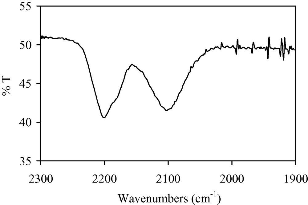
Black amorphous thin films of Mo(TCNE)x are prepared via CVD of Mo(C6H5CH3)2 and TCNE precursors. They are very adherent on Si(001) wafers. X-ray photoelectron spectra show the presence of Mo, C, N, and O. The presence of oxygen (0.3 at.%) is assigned to surface contamination. The N/Mo atomic ratio is found to be 7.3, a value in rather good agreement with a 1 Mo/2 TCNE stoichiometry (MoC12N8). The Mo3d5/2 and Mo3d3/2 lines are located at 228.7 and 231.8 eV, respectively (areas ratio: 1.33, in reasonable agreement with the theoretical value of 6/4). The Mo3d5/2 has a binding energy very close to that for MoII complexes, such as Mo(C5H5)(CO)3Cl (228.7 eV) and Mo(C5H5)(CO)3[Sn(CH3)3] (228.5 eV) [32]. The N1s signal (399.2 eV) has a binding energy consistent with the presence of TCNE•–. This value is in good agreement with that obtained for [MnIII(TPP)][TCNE], 2 C6H5CH3 (TPP = meso-tetraphenylporphyrin), i.e. 399.1 eV (trans-μ-TCNE•– moiety) [33]. Infrared spectra show two νCN broad bands at 2212(s) and 2113(m) cm–1 (Fig. 14), close to those observed for [Mn(C5Me5)(CO)2][TCNE] (2205 and 2125 cm–1) in which TCNE is trans-μ-N-bound to manganese(II) [34]. Moreover, no νCH bands (3070–2800 cm–1 region) corresponding to the presence of toluene rings are observed. SEM images (Fig. 15) evidence a cracked film on which roughly spherical agglomerated grains are randomly dispersed (average size of the spherical grains: 1.5 μm). Fig. 16 shows the hysteresis loop (magnetization vs. applied magnetic field) at 2 K. The sample nearly saturates for an applied magnetic field of 50 kOe and a coercive field of ~20 Oe is observed.
IR spectrum of Mo(TCNE)x thin films (νCN region).
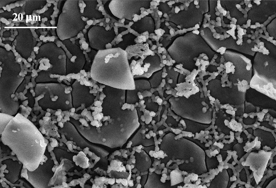
SEM image of Mo(TCNE)x thin films.
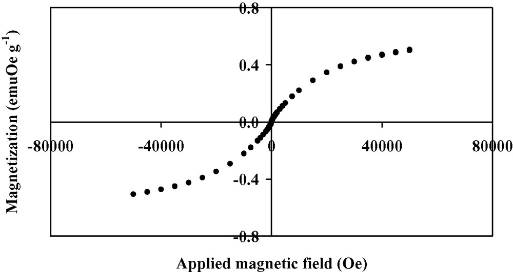
Hysteresis loop at 2 K for Mo(TCNE)x thin films.
3.2 Conductors based on bis(dithiolene) complexes as thin films
3.2.1 Introduction
Homoleptic dithiolene complexes ML2 (L: 1,1-, 1,2- or 1,3-dithiolene ligand) have been extensively considered as a key unit to build up molecule-based materials exhibiting a metallic behavior [35]. To obtain a metallic state, partial filling of the conduction band is required. This may be obtained either through partial oxidation, as in non-integral oxidation state salts, or through partial charge transfer, as in donor–acceptor adducts. The (cation)x[M(dithiolene)2] salts are prepared either by chemical or electrochemical oxidation of the appropriate (cation)[M(dithiolene)2] salt. The D[M(dithiolene)2]y (D: donor molecule) compounds can be prepared either by electrochemical oxidation of the donor molecule in the presence of the appropriate (cation)[M(dithiolene)2] salt or by metathesis reaction between the appropriate D(anion) and (cation)[M(dithiolene)2] salts.
We present in the following 3.2.2 and 3.2.3 paragraphs, the preparation of electrodeposited thin films of two Ni(dithiolene)2-based conductors, namely the non-integral oxidation state salt [(n-C4H9)4N]2[Ni(dcbdt)2]5 (dcbdt2–: 4,5-dicyanobenzene-1,2-dithiolato), and the donor–acceptor adduct TTF[Ni(dmit)2]2 (TTF: tetrathiafulvalene; dmit2–: 1,3-dithiole-2-thione-4,5-dithiolato).
3.2.2 Electrodeposited films of [(n-C4H9)4N]2[Ni(dcbdt)2]5
[(n-C4H9)4N]2[M(dcbdt)2]5 (M = Ni, Au) single crystals can be prepared as thin plates (3 × 0.3 × 0.05 mm3) on the surface of a platinum anode, by electrocrystallization from the corresponding [(n-C4H9)4N][M(dcbdt)2] complex under galvanostatic conditions [14,36]. Both compounds present a triclinic structure (P-1) showing stacks of pentamerized M(dcbdt)2 units along [–210]. The electrical conductivity measured along the long axis [–210] of the elongated-shaped crystals denotes a semi-conducting behavior (σRT = 0.13 S cm–1 and activation energy Ea = 0.176 eV for M = Ni; σRT = 10 S cm–1 and Ea = 0.027 eV for M = Au).
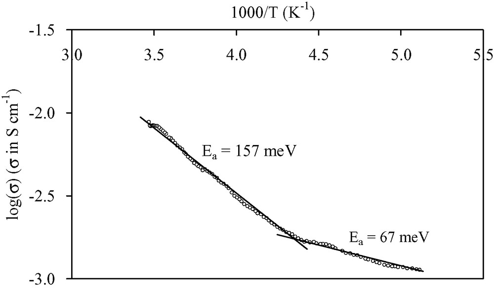
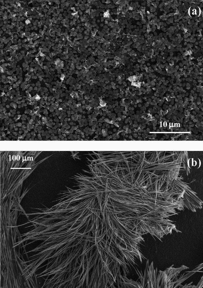
Thin films of [(n-C4H9)4N]2[Ni(dcbdt)2]5 are obtained by galvanostatic electrolysis on a silicon wafer in a one-compartment cell containing a dichloromethane solution of [(n-C4H9)4N][Ni(dcbdt)2]. The films uniformly cover the substrate surface. X-ray powder diffraction data evidence a highly oriented film (Fig. 17). Refinement of the collected data gives the following crystallographic parameters: a = 7.999(8) Å, b = 17.271(2) Å, c = 22.490(3) Å, α = 69.01(1), β = 89.08(1), γ = 78.90(1), to be compared with a = 8.000(1) Å, b = 17.288(3) Å, c = 22.490(4) Å, α = 69.181(8), β = 89.161(12), γ = 78.14(1) obtained from single crystal study [37]. The very good agreement of the lattice parameters confirms the 2:5 stoichiometry and shows that the deposition process does not affect the structural arrangement of the compound although the very weak intensity of the diffraction lines other than (001) and (002) may limit the precision of the measurement. The growth of the film is then found to be highly anisotropic, the ab-plane being parallel to the wafer surface. Electron micrographs evidence that the film is made of thin platelets (30–55 μm long, 1–8 μm width, thickness <1 μm) randomly distributed on the substrate surface (Fig. 18a). Moreover, a SEM side view of a segment of the film peeled off from the surface allows us to evaluate the thickness at ~10 μm. Raman spectra performed on the film (Fig. 19a) and on the precursor material (Fig. 19b) exhibit almost the same characteristic vibrational bands. Bands at 405(m), 362(s) and 347(s) cm–1 are, respectively, assigned to C–S stretching, Ni–S stretching, and out of phase deformation of the five-membered rings connected to the nickel [38,39]. It should be noted that medium intensity Raman signals appearing at 1546 cm–1 (aromatic C=C stretching modes) and 2220 cm–1 (CN stretching modes) for the precursor compound shift to higher frequencies, that is 1557 and 2225 cm–1, respectively, for the film. This frequency shift is in agreement with the decrease of the average value of the charge of the Ni(dcbdt)2 moiety [Ni(dcbdt)2– → Ni(dcbdt)20.4–], as previously reported in the case of thin films of [(n-C4H9)4N]0.9[Ni(dmid)2] [7]. From the infrared spectrum, we see that, also due to the charge change of the complex in the deposit relatively to [Ni(dcbdt)2]–, carbon–hydrogen stretching vibrations of the phenyl groups are shifted from 3061 cm–1 in the starting complex to 3067 cm–1 in the film (Fig. 20). As expected, CH stretching modes of butyl groups of the [(n-C4H9)4N]+ cations (2850–2965 cm–1) remain unchanged after partial oxidation of [(n-C4H9)4N][Ni(dcbdt)2]. The nitrile vibration modes are present at 2226 cm–1 in the infrared spectrum of the deposit, a value almost identical to that observed in the Raman spectrum. The electrical conductivity of [(n-C4H9)4N]2[Ni(dcbdt)2]5 thin films is about 1.2 × 10⁻² S cm–1 at room temperature and follows a thermally activated semiconducting behavior. The plot of log(σ) versus 1/T shows an activation energy of 157 meV in the range 295–230 K (Fig. 21). This value is reduced to 67 meV below 230 K.

X-ray diffraction pattern for electrodeposited [(n-C4H9)4N]2[Ni(dcbdt)2]5 thin films.
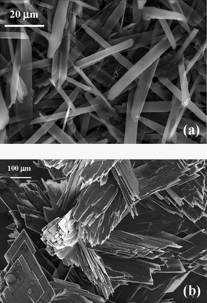
SEM images of deposits of [(n-C4H9)4N]2[Ni(dcbdt)2]5 under galvanostatic conditions (a), potentiostatic conditions (b).
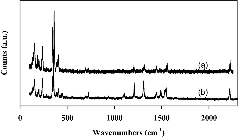
Raman spectra of deposits of [(n-C4H9)4N]2[Ni(dcbdt)2]5 (a) and of the starting [(n-C4H9)4N][Ni(dcbdt)2] complex (b).

Infrared spectrum of deposits of [(n-C4H9)4N]2[Ni(dcbdt)2]5.
Conductivity as a function of reciprocal temperature for electrodeposited [(n-C4H9)4N]2[Ni(dcbdt)2]5.
3.2.3 Electrodeposited films of TTF[Ni(dmit)2]2
TTF[Ni(dmit)2]2 belongs to the donor–acceptor family of compounds. Within the final material, the charge transfer between the TTF donor molecule and the [Ni(dmit)2] acceptor complex was found to be 0.8 from diffuse X-ray scattering experiments and band structure calculations [40]. The structure of TTF[Ni(dmit)2]2 consists of segregated stacks of TTF and [Ni(dmit)2] units. On single crystal, its room-temperature conductivity is ~300 S cm–1 at ambient pressure along [010]. The conductivity behavior is metallic down to 4 K. Moreover, this compound undergoes a complete transition to a superconducting state at 1.62 K under a hydrostatic pressure of 7 kbar [41].
Electrodeposition of TTF[Ni(dmit)2]2 is carried out with intrinsic Si(001) as anode and a platinum wire as cathode in an H-shaped electrochemical cell (Table 2). XPS data confirm the 1 TTF/2 [Ni(dmit)2] stoichiometry for the films. Fig. 22 shows the XPS S2p line measured on TTF[Ni(dmit)2]2 thin films. The experimental lineshape can be satisfactorily decomposed in three contributions. The most intense line, with a binding energy of 163.5 eV, corresponds to C–S–C, as already reported for TTF derivatives [42]. We assign the 161.8 and 165.3 eV lines to C–S–Ni and C=S, respectively, based on their relative intensities. In the nominal formula TTF[Ni(dmit)2]2, there are 12 C–S–C, 8 C–S–Ni and 4 C=S bonds, which results in a ratio 3:2:1. From the fit the intensity ratio between the C–S–C and C–S–Ni contributions is 1.4, in excellent agreement with the nominal 1.5 value. For a molar ratio of TTF/Ni = 3 within the electrochemical solution, electron micrographs of a covered area show a dense film made of roughly spherical grains with sizes ranging from 0.6 to 1 μm (Fig. 23a). For a molar ratio of TTF/Ni = 0.75 and whatever the current density value, fibers are observed (> 100 μm long and 1–5 μm width, Fig. 23b). Fig. 24 shows the infrared spectrum (absorbance vs. wavenumbers) of the electrodeposited material. It confirms the presence of both TTF and Ni(dmit)2 moieties within the films. The peak at 3081(w) cm–1 corresponds to the CH ethylenic stretching vibrations for TTF. The band located at 509(m) cm–1 corresponds to the symmetric stretching vibration of the two carbon–sulfur single bonds in the S2C=S fragment of dmit [43]. The characteristic doublet present in all compounds containing the M(dmit)2 moiety, displays maxima at 1051(m) and 1071(s) cm–1, respectively. The higher frequency peak of the doublet (1071 cm–1) is assigned to the stretching vibration of carbon–sulfur double bond in the terminal S2C=S fragment of dmit, while the lower one (1051 cm–1) corresponds to the Fermi resonance peak between overtones of symmetric stretching vibration of two carbon–sulfur single bonds in the S2C=S fragment of dmit and the higher frequency [43]. For [N(n-C4H9)4][Ni(dmit)2], the doublet exhibits maxima at 1063 and 1030 cm–1 [43]. The higher frequencies for the deposit confirm the less anionic character of the Ni(dmit)2 skeleton. The Raman spectrum shown on Fig. 25 is in excellent agreement with that reported for TTF[Ni(dmit)2]2 single crystals [44]. Low-frequency bands are vibration modes related to the Ni(dmit)2 entity: 137(s), 343(vs), 361(s), 492(s), and 1334(w) cm–1 [39,45]. The C=C stretching modes at 1430(m), 1471(sh), and 1509(w) cm–1 are related to the TTF moiety [46]. The lower frequency line (1430 cm–1) involves a large contribution of the central carbon–carbon double bond in TTF (71%). This band, whose position is very sensitive to the amount of charge transfer (1518 cm–1 for neutral TTF and 1420 cm–1 for TTF+), allows us to determine a charge transfer of about 0.86 [47]. This value is in relatively good agreement with that obtained from band structure calculations, i.e. 0.80 [40]. The two other Raman lines at 1471 and 1509 cm–1 are also lower compared to those for neutral TTF (1530 and 1555 cm–1), confirming the cationic character of the TTF moiety. Fig. 26 shows the electrical behavior of the electrodeposited material: the ratio resistance at a given temperature (T) over resistance at 300 K [R(T)/R (300 K)] is reported as a function of the temperature. The samples exhibit a metallic behavior down to ca. 14 K, temperature at which the resistance slightly increases. At 14 K, the resistance is around 4.3 times smaller than the resistance at 300 K, and is still four times smaller at 4.5 K. Such a behavior is totally reversible, when warming back to room temperature. Such a reversibility has also been observed on single crystals of TTF[Ni(dmit)2]2 [48], but with a resistance at 4.4 K ~500 times smaller compared to the one at 300 K. Moreover the conductivity value is of ~12 S cm–1 at room temperature, and larger than 50 S cm–1 at 14 K.
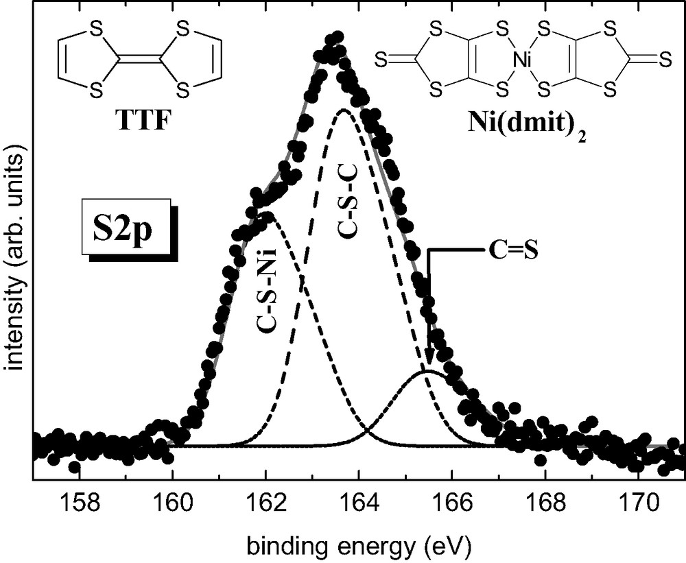
XPS S2p line (black dots) measured at room temperature of a TTF[Ni(dmit)2]2 thin film. Also shown is a least-square fit (Gaussians), after a Shirley-type background subtraction, where each line (dashed) is composed of a spin–orbit split doublet with an energy separation ESO and a branching ratio B. The addition of the three lines results in the continuous gray line. Results from the fit: E(C–S–Ni) = 161.8 eV, E(C–S–C) = 163.5 eV, E(C=S) = 165.3 eV, Γ = 1.5 eV, ESO = 1.1 eV and B = 0.5.
SEM images of deposits of TTF[Ni(dmit)2]2 elaborated at 1.5 μA cm–2 (a: TTF/Ni = 3; b: TTF/Ni = 0.75).

Infrared spectrum of electrodeposited TTF[Ni(dmit)2]2 thin films.
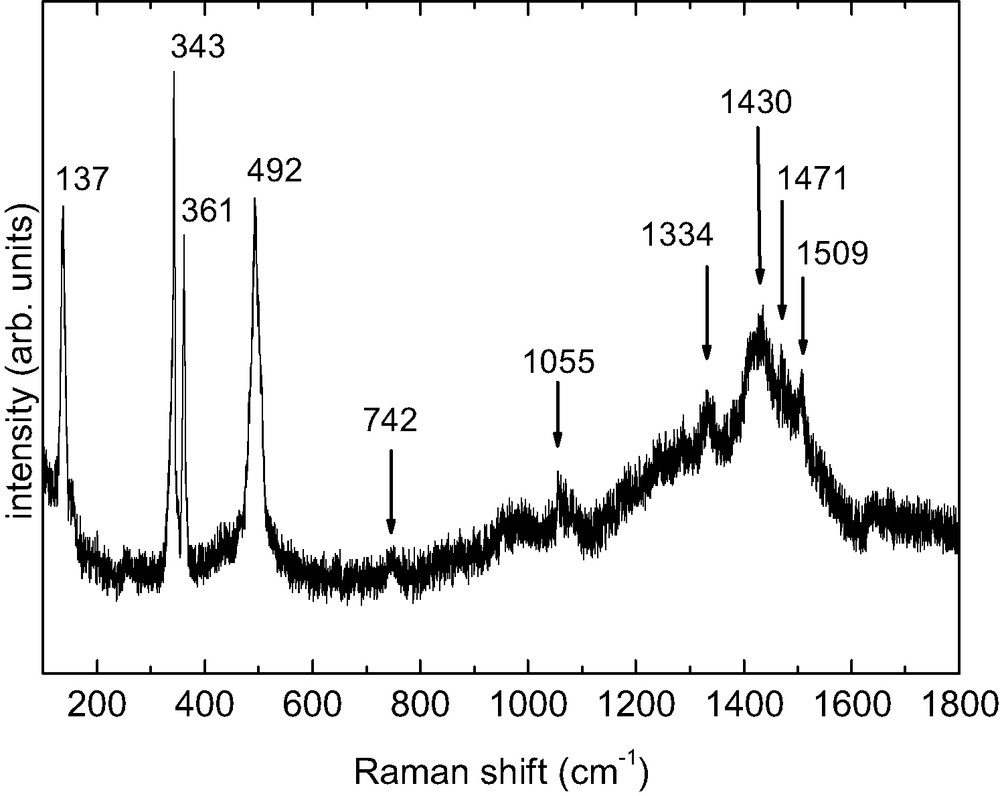
Raman spectrum of electrodeposited TTF[Ni(dmit)2]2 thin films.
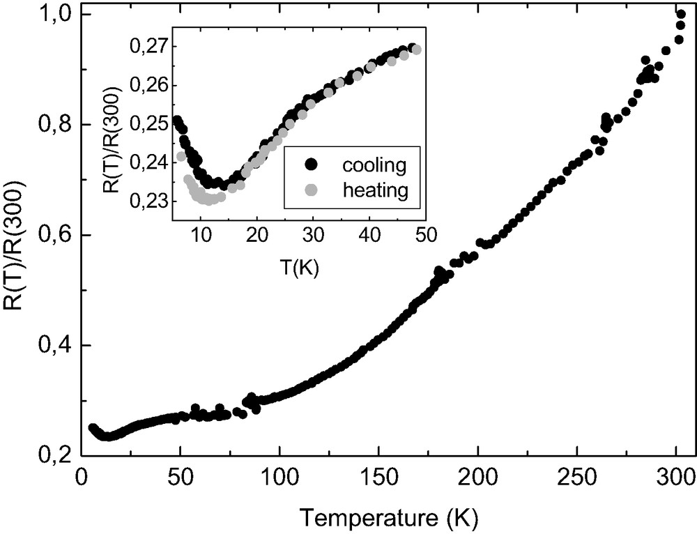
Resistance as a function of temperature for electrodeposited TTF[Ni(dmit)2]2 thin films.
4 General discussion
4.1 M(TCNE)x magnets
Previously to this work, we had reported the use of silicon wafers as substrates for growing TTF-based molecular semiconductors. During these studies, we have observed that [TTF][TCNQ] (TCNQ = tetracyanoquinodimethane) films appear as platelets (3 × 1 μm) and needles (diameter < 0.3 μm) [49], while [TTF-(OH)TEMPO][TCNQ] (TEMPO = N,N,N-trimethyl-1-oxyl-2,2,6,6-tetramethylpiperidin-4-yl) ones exhibit a micro-needle morphology (0.5–2 μm in length, 0.1–0.2 μm in diameter) [42]. Moreover, these films were found to be very adherent on the Si surface. The CVD-grown thin M(TCNE)x magnets described in this paper exhibit a very different morphology. Whatever the metal nature, electron microgaphs evidence continuous films showing more or less cracks (Figs. 1,6,12, and 15). However, these latter do not affect the adherence of the films onto the silicon surface. Thus, silicon is the substrate of choice due to its low weight over surface ratio, its wide use in the electronic domain and due to the fact that materials vapor deposited on it, keep their interesting magnetic properties.
All M(TCNE)x deposits display a two-absorption peak pattern for νCN stretching modes (~2100 and ~2200 cm–1, Table 3). Moreover, a shoulder in the range 2140–2180 cm–1 is occasionally encountered. Therefore, it is concluded that TCNE is present as μ2-, μ3-, or μ4-TCNE•– [16]. It is also to be noticed that the complex and broad nature of the absorptions suggests that mixtures of bonding motifs are present. Furthermore, X-ray photoelectron surface analysis evidences both the presence of monoreduced TCNE (thus confirming infrared data), and the presence of the metal center in a low-oxidation state (typically, MII). According to the literature, only M(TCNE)x, y CH2Cl2 (M = Mn, Fe) magnets give X-ray powder patterns. However, they have never been indexed. M(TCNE)x, y S are proposed to be composed of [TCNE•–]s being bound to up to four Ms most likely linearly, although some may be bent and each TCNE•– is planar [16]. Because of the expected hexacoordination of M(II), each TCNE•– may bind to three M(II)s, although some coordination sites may be occupied by solvent molecules [16]. The CVD-grown M(TCNE)x phases described here show no diffraction line within the range d = 7.5–3.5 Å (d: inter-reticular distance). We have explored the use of X-ray absorption spectroscopy for structural investigations. Indeed, EXAFS has been widely used for studying Prussian blue-like materials [26]. For performing such an EXAFS study within the M(TCNE)x series, the Cr(TCNE)x phase, which displays a relatively large air stability, has been selected. The structural parameters are in agreement with an hexacoordination of Cr(II). The mean Cr–N distance is of 2.03 Å and the Cr–N–C angle is of about 160° (Scheme 4).
Summary of the νCN IR absorption data for vapor deposited M(TCNE)x films
| Compound | νCN (cm–1) |
| V(TCNE)x (as-deposited) | 2105(s), 2192(m) |
| V(TCNE)x (after annealing) | 2106(s), 2145(sh), 2195(m) |
| V(TCNE)x (after annealing and 1 h air exposure) | No change compared to the above data |
| Cr(TCNE)x | 2116(s), 2202(m) |
| Nb(TCNE)x | 2102(s), 2180(sh), 2200(m) |
| Mo(TCNE)x | 2113(s), 2212(m) |
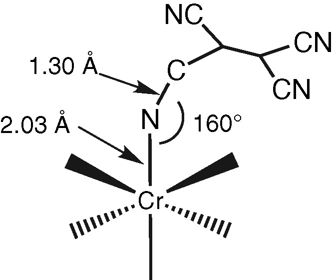
Basic model for the chromium environment in Cr(TCNE)x magnets.
All M(TCNE)x compounds prepared as thin films by CVD exhibit a spontaneous magnetization at low temperature (Table 4). As-deposited V(TCNE)x exhibits a field-dependent magnetization between 5 and 300 K, and saturates to about 18 emuOe g–1 at 5 K and 800 Oe. Assuming x ~2 and a Landé factor of g = 2, this value is in good agreement with antiferromagnetic coupling between S = 3/2 V(II) and two S = 1/2 TCNE•– species (i.e. Stotal = 1/2) [18]. The saturation magnetization temperature dependence can be fit to the Block Law, MS = MS(0) [1–B T3/2], of the spin wave theory [50], with MS(0) = 18.2 emuOe g–1 and B = 1.7 × 10⁻⁴ K–3/2. Using B = 0.0587(kB/2JStotal)3/2/Stotal, the average exchange energy, J/kB, is 80 cm–1. This value is in rather good agreement with that reported for V(TCNE)x magnets obtained by co-sublimation of V(CO)6 and TCNE (100 cm–1) [22]. The hysteresis loop recorded at 300 K shows a coercive field of 80 Oe and a saturation magnetization of ~2.5 emuOe g–1 (Table 5). Thermal treatment (at 343 K for 10 h) reduces the magnetization by a factor of about 40 (Table 5). Further air exposure (1 h) does not destroy magnetic ordering at room temperature (Table 5). However, reduction in the magnetization value by a factor of about 5 is observed (with respect to the thermally treated sample kept under an argon atmosphere). The magnetic susceptibility of the Cr(TCNE)x films has been measured between 2 and 300 K (Fig. 9). The temperature dependence of the susceptibility obeys the Curie–Weiss law above 80 K with a θ value of –95 K, a larger negative value than that observed for Cr(TCNE)x, 0.5 C6H5CH3 prepared from Cr(naphthalene)2 and TCNE in toluene solution (θ = –75 K) [29]. Consequently, the magnetic interaction between the spin centers is strongly antiferromagnetic. Fig. 10 shows the hysteresis loop (magnetization versus applied magnetic field) at 2.5 K. The major feature in this data is the absence of saturation for fields up to 65 kOe. However, a coercive field of ~100 Oe at 2.5 K is clearly evidenced as shown in the insert in Fig. 10. We conclude that, at this temperature, magnetic ordering exists in the sample. At 2.5 K, the magnetization value for an applied field of 65 kOe is about 11 emuOe g–1. Assuming a Cr(TCNE)x ~ 2 composition, an independent S = 2, 1/2, 1/2 system should have a saturation magnetization of ~36 emuOe g–1. Strong antiferromagnetic couplings, as evidenced by the large negative θ value, may explain the reduced magnetization values.
Magnetic data for vapor deposited M(TCNE)x films at 5 K (V), 2.5 K (Cr, Nb), 2 K (Mo)
| Compound | Saturation magnetization (emuOe g–1) | Saturation induction (Oe) | Coercive field (Oe) |
| V(TCNE)x (as-deposited) | 18 (a) | 800 | 10 |
| Cr(TCNE)x | 11* (a) | – | 100 |
| Nb(TCNE)x | 6 × 10⁻⁴ (b) | 20,000 | 200 |
| Mo(TCNE)x | 0.5 (a) | 50,000 | 20 |
Magnetic data for vapor deposited V(TCNE)x films at 300 K
| Compound | Saturation magnetization (emuOe g–1) | Saturation induction (Oe) | Coercive field (Oe) |
| V(TCNE)x (as-deposited) | 2.5 | 800 | 80 |
| V(TCNE)x (after annealing) | 5.9 × 10⁻² | 2500 | 50 |
| V(TCNE)x (after annealing and 1 h exposure to air) | 1.2 × 10⁻² | 1500 | 50 |
The M(TCNE)x, y solvent complexes with a second-row transition metal have never been described before. The reaction of Nb(iPr2-dad)3 in the presence of TCNE in refluxing toluene for 20 h leads to a low amount of black precipitate for which the results from the elemental analysis are not interpretable. Its infrared spectrum evidences a strong band at 2199 cm–1 assigned to coordinated TCNE and the characteristic vibration modes of the diazabutadiene ligands. Furthermore, the reaction of Nb(η6-mes)2 (mes: mesitylene) in the presence of TCNE in toluene at room temperature leads instantaneously to a black precipitate. However, the solution is stirred at room temperature for a further 10 h to ensure total reaction. The precipitate is analyzed as Nb(TCNE)1.1·0.4 C7H8. Its infrared spectrum in the νCN region exhibits two broad absorptions at 2092(s) and 2198(s) cm–1, in agreement with coordinated TCNE•– species. Moreover, preliminary magnetic measurements evidence that the compound exhibits a spontaneous magnetization at 2 K (coercive field: 100 Oe). Therefore, Nb(η6-mes)2 complex seemed to be the precursor of choice for growing thin films of Nb(TCNE)x using the CVD technique. Although vaporization of the precursor was efficient, no deposit is obtained, at least in the explored conditions. Nb(TCNE)x as thin film can be obtained from the Nb(iPr2-dad)3 precursor (Table 1). Infrared spectra of the deposits display strong CN modes and small features corresponding to a low amount of diazabutadiene ligands remaining on the niobium atoms. The films exhibit a spontaneous magnetization at 2.5 K and a coercive field of ~200 Oe. Finally, Mo(TCNE)x thin films obtained from the Mo(C6H5CH3)2 precursor (Table 1) also behave as permanent magnets at 2 K and display a coercive field of ~20 Oe.
As a conclusion to this section, we have shown the feasibility of producing thin films of M(TCNE)x molecule-based magnets by CVD (M: first- or second-row transition metal, namely, V, Cr, Nb, Mo). There are found to be relatively adherent on the silicon surface and, by suppressing the deleterious effect of the solvent (observed on solution-grown M(TCNE)x, y solvent compounds), they all exhibit a spontaneous magnetization (at low temperatures for Cr, Nb, and Mo, and in the temperature range 5–300 K for V).
4.2 Molecule-based conductors on Si
4.2.1 Non-integral oxidation state salt [(n-C4H9)4N]2[Ni(dcbdt)2]5 as thin films
Thin films of [(n-C4H9)4N]2[Ni(dcbdt)2]5 are obtained by electrolysis of a dichloromethane solution of [(n-C4H9)4N][Ni(dcbdt)2] on a silicon wafer used as anode (galvanostatic or potentiostatic conditions). Films mainly form on the non-polished face of the silicon electrode. Elemental analysis of a sample of film scratched from the surface gives the following results: %C = 49.90; %H = 2.77; %N = 11.05. These values are in good agreement with the data calculated for [(n-C4H9)4N]2[Ni(dcbdt)2]5 (%C = 50.18; %H = 3.46; %N = 11.49). Therefore, the same 2:5 stoichiometry is obtained within the films. Under galvanostatic conditions, electron micrographs evidence that the film is made of thin platelets (30–55 μm long, 1–8 μm width, thickness < 1 μm) randomly distributed on the substrate surface (Fig. 18a). This thin film morphology is in sharp contrast with the dendritic growth reported for [(n-C4H9)4N]0.9[Ni(dmid)2] on a Pt metal foil [7] and also for [(n-C4H9)4N]2[Ni(dcbdt)2]5 platelets on platinum wires [14], both at high current densities (i.e. 25 μA cm–2). As a matter of fact, in our case, much lower current densities (0.5 μA cm–2) are applied and could favor the growth of long platelets or needles. A SEM side view of a segment of the film peeled off from the surface allows us to evaluate the thickness at ~10 μm. As expected, under potentiostatic conditions (Eapp = 1.0 V vs. SCE), that is at higher growth rates than in galvanostatic conditions, the quantity of material appears much higher. Moreover, the quality of micro-crystals is also lower (Fig. 18b). The electrical conductivity of [(n-C4H9)4N]2[Ni(dcbdt)2]5 thin films (elaborated under galvanostatic conditions) is about 1.2 × 10⁻² S cm–1 at room temperature and follows a thermally activated semiconducting behavior. The plot of log(σ) versus 1/T shows an activation energy of 157 meV in the range 295–230 K (Fig. 21). This value is reduced to 67 meV below 230 K. A similar semiconducting behavior was observed on single crystals with very similar activation energy values (176 meV at high temperatures and 68 meV below 250 K) [37]. The origin of this noticeable change in the activation energy is not yet clear and may be associated to a phase transition. The room temperature conductivity of the film is one order of magnitude lower than that of single crystals (0.15 S cm–1). The [–210] direction, which is the stacking direction and the direction of highest conductivity, also corresponds to the direction of the long axis of the needle-like crystals [37]. As electron micrographs show that the grown needles lay on the surface, the direction of highest conductivity is part of the plane in which the film conductivity is measured. This feature, the contributions of other directions within the crystallites, and the polycrystalline nature of the film, which generates grain boundaries, account for the lower conductivity value of the film versus that of the crystal. However, the conductivity ratio between single crystal and film is rather low and indicative of a more than one-dimensional system.
4.2.2 Charge transfer salt TTF[Ni(dmit)2]2 as thin films
Deposits of TTF[Ni(dmit)2]2 are obtained by electrolysis of an acetonitrile solution of TTF and [(n-C4H9)4N][Ni(dmit)2] on a silicon wafer used as anode (galvanostatic conditions, see Table 2). Deposits form on both the polish and the non-polished faces of the silicon electrode. They are adherent and insensitive towards an air exposure. When a molar ratio TTF/Ni = 3 is used (at 1.5 μA cm–2), a dense film made of roughly spherical grains (size: 0.6–1 μm) is observed (Fig. 23a). About 15% of the surface remains non-covered. To evaluate the thickness of the films, side views of the sample were difficult to perform. However, assuming a ‘monolayer’ of grains (as observed on SEM), a thickness of the order of magnitude of 1 μm seems reasonable. When a molar ratio TTF/Ni = 0.75 is used (at 0.8, 1.5, or 2.5 μA cm–2), simple eye observation shows that the silicon surface is poorly covered. Within the covered areas, electron micrographs evidence the presence of severely aggregated micro-fibers (several hundred micrometers long, 1–5 μm wide, Fig. 23b). For higher current densities (1.5 and 2.5 μA cm–2), these fibers have a certain tendency to be aligned. However, the effect of stoichiometry on morphology and surface covering is not yet understood. Electrodeposited TTF[Ni(dmit)2]2 thin films (elaborated at 1.5 μA cm–2 with excess TTF) have a metallic behavior down to ca. 14 K, temperature at which the resistance slightly increases. Moreover, this behavior is totally reversible, when warming back to room temperature, as previously observed on TTF[Ni(dmit)2]2 as single crystals [48]. Taking into account the size and shape of the studied sample, this leads to a conductivity of ca. 12 S cm–1 at room temperature, and larger than 50 S cm–1 at 14 K. Obviously, these values are much lower than the values reported for the conductivities on single crystals (300 S cm–1 at 300 K, and 1.5 × 10⁵ S cm–1 at 2 K) [48]. Nevertheless, it should be pointed out here that, whatever the substrate, the conductivity of thin films is usually very low, as observed for [TTF][TCNQ] (0.4 S cm–1) [49], or (BEDT-TTF)(ClO4)x (10–3 S cm–1) [51]. Moreover, these thin films usually exhibit a semiconducting behavior, due in part to grain boundaries and/or heterogeneous morphologies. However, transparent composite films made of polycarbonate/θ-(BET-TTF)2Br, 3 H2O have been recently described and showed metal-like transport properties down to liquid helium temperature, with σRT ~100 S cm–1 [52]. Nevertheless, it is worth noting that our films are, to our knowledge, the first example with a dithiolate complex, displaying a metallic behavior down to very low temperature.
5 Conclusion
We have shown the feasibility of producing thin films of molecule-based magnets by CVD, and thin films of molecule-based conductors by electrodeposition. We have explored the use of silicon substrates, whose importance in the electronic domain is obvious. M(TCNE)x magnets are grown from the gas phase reaction of an organometallic complex and TCNE. These materials present potential magnetic shielding and inductive applications [53,54]. Thin films of two molecule-based conductors, namely [(n-C4H9)4N]2[Ni(dcbdt)2]5, and TTF[Ni(dmit)2]2 have been processed by using the electrodeposition technique. TTF[Ni(dmit)2]2 as thin films exhibits a well-defined metallic behavior down to about 14 K. The metallic behavior evidences that low inter-grain conduction energy barriers are achieved, in contrast with most thin films of highly-conducting materials reported to date. Since TTF[Ni(dmit)2]2 undergoes a superconducting transition (critical temperature:1.6 K under 7 kbar hydrostatic pressure), our results open the possibility of preparing superconducting thin films of other molecule-based materials, in spite of their polycrystalline morphology, based on the well-known and extensively-used electrodeposition technique.
Acknowledgements
H. Casellas thanks the French government for funding her Ph.D. by a MENESR grant. J.-P. Savy thanks the Fond Social Européen (FSE) for a grant. The authors gratefully thank Dr. F. Villain for X-ray absorption spectra, Dr. A. Zwick for Raman measurements, Dr. F. Senocq for XRD data, Dr. J. Fraxedas for X-ray photoelectron spectra, Dr. A. Mari for magnetic measurements, Professor M. Almeida for supplying the [(n-C4H9)4N][Ni(dcbdt)2] starting complex, and V. Collière for SEM micrographs. D. Bérail from Motorola is acknowledged for supplying supports for conductivity measurements.