

1 Introduction
Ordered mesoporous materials synthesized through surfactant templating exhibit high porosity with channel or interconnected pore structures of amorphous silicate framework, uniform apertures in the range of 2–30 nm diameter and large surface area of ≤ 1000 m2/g [1,2]. They have expanded the pore size related applications of zeolite molecular sieves from microporous to nanoporous. Their intrachannel and intrapore voids provide the confined space to accommodate nanostructured molecules and clusters [3,4], and the reactive surface hydroxyl groups on the intrachannel and intrapore surface can be chemically modified through silynation [5]. In addition to the original 2D-hexagonal MCM-41 (P6mm) and 3D-bicontinuous cubic (MCM-48 (
Formation of ordered mesoporous materials takes place under alkaline, acidic or neutral conditions via the cooperative interaction of organic surfactants and inorganic species through electrostatic attraction or hydrogen bonding [10,11]. The morphological variability achievable covers powder, fiber, film, hard sphere, hollow, rod and monolith [12–15]. Besides powder, thin film has attracted the most attention because of their potential uses in chemical sensors, membrane separation, optical devices and electronic devices [6,16–24].
Continuous thin films of surfactant-templated mesoporous silica were detected growing either in self-support form [25] or on top of porous or dense support [26]. Preparation methods including sol–gel coating and hydrothermal synthesis since first being reported in 1996 were reviewed recently [27–29]. Synthesis of such thin films is preferably under acidic condition and has the growth from a homogeneous solution of reactants as well as being induced by rapid solvent evaporation from a sol precursor coated on a solid support. Through an epitaxial-like growth, the mesochannels can be aligned under a controlled reactant flow [30] or on a modified anisotropic surface of a glass substrate [31] or on a specific crystalline plane i.e. (110) plane of a silicon wafer [32]. With a bulk alignment of mesochannels in a continuous thin film, guest molecules and clusters can be incorporated and aligned in confined directions, and thus create orientation-dependant optical, electronic, optoelectronic or magnetic properties and applications. However, the epitaxial-like growth takes more time than the solvent evaporation methods. In the latter, the sol solution usually consists of soluble silica and surfactant in ethanolic and aqueous solution with an initial concentration of surfactant (co) much less than the critical micelle concentration (cmc). The silicate species in the precursor sol undergo hydrolysis and condensation to form a gel. During and after the coating process, the surfactant concentration increases through the evaporation of solvent. When the concentration of surfactants reaches cmc, surfactant ions or molecules will form micelles and thus enhance the growth of organic-inorganic hybride mesostructures. The degree of condensation of silicate moieties and the rate of solvent evaporation play critical roles during self-assembly and thus affecting the ordering of the final mesostructure. Sol–gel based dip- or spin-coating and aerosol-associated deposition are usually employed to rapidly produce continuous mesoporous films on substrates in large area and controlled thickness [33,23]. Interfacial bonding between the coated film and the substrate can take place through hydroxyl condensation by heat treatment, and the resulting film will attach itself to the substrate firmly. Grosso et al. [34] recently reported that the final mesostructure and texture of silica and titania films are controlled by the specific chemical and processing parameters. They suggested that the mechanism of self-assembly is through concentration gradients as well as the film’s composition in quasi-equilibrium with its environment.
Mechanical strength and stability of mesoporous films are important prerequisites for their optical and electronic applications, and good mechanical properties can, in turn, be achieved through well-organized film texture [35,36]. Furthermore, the scope of applications of mesoporous films is closely associated with their pore properties such as pore size, porosity and pore structure [37–39]. Mesoporous silica films, with their dielectric constant as a function of porosity and reasonable mechanical strength derived from the ordered pore structure [23,37], are considered as one of the most promising low-dielectric materials for ultralarge-scale integration (ULSI) device. Gas transport of these films was found to be somewhat affected by the randomness of the ordered domains in the mesoporous membrane [38]. Furthermore, the uniform thickness and proper density of the nanoporous coating play a key role in the film’s anti-reflection of light [39]. In this paper, we will address and further review the various characterization methods of mesoporous silica films. Since the pore structure and film texture of supported thin films were found to be affected by substrate, and such films are usually used together with its substrate in applications, it is desirable to perform the characterization using on-substrate techniques for supported thin films instead of the characterization of films detached from their substrates. Optical and electronic applications of supported thin mesoporous silica films on silicon wafer and glass supports will also be discussed in this report.
2 Characterization
Porosity of nanoporous films on flat substrate has been known to be derived from refractive index obtained from ellipsometric porosimetry or n&k analyzer [40] and film density obtained from specular X-ray reflectivity (XRR) [41]. To measure pore sizes and pore size distribution (PSD), physical adsorption of an inert gas on dehydrated samples has been considered capable of avoiding the effect of water uptake on the hydrophilic mesoporous materials [42]. Atomic force microscope (AFM), scanning electron microscopy (SEM) and transmission electron microscopy (TEM) have been used to probe the film local structure. While, for detailed structural analysis of films, grazing incident X-ray diffraction (GIXD) and small-angle neutron scattering have been used for free-standing and supported mesoporous films [36,43]. In this short review, we will present the characterization of mesoporous films through some limited means concomitant with the potential applications of these materials in the electronic and optical fields.
2.1 Krypton adsorption
For quite a while physical adsorption of gases has been considered as a standard method to measure the pore properties of micro- and mesoporous materials [44]. Most of the studies on powdery nanoporous samples suggested the use of conventional BJH analysis as the method to estimate the PSD from the adsorption isotherm of N2 or Ar. BJH analysis needs two pieces of information: the relationship between pore size and its capillary evaporation (or condensation) pressure, and the change of adsorbed film thickness with pressure in open pores. By studying mesoporous materials of ordered cylindrical mesochannels, the corrected Kelvin equation, modified Broekhoff–de Boer (BdB) method or a semi-molecular approach (NLDFT, the non-local density functional theory calculation) were found recently to be more appropriate to provide the required information for the first part in BJH analysis [42,44–47]. While the experimental t-curves of N2 and Ar physisorption on an non-porous standard or the calculated values from Frenkel–Halsey–Hill (FHH) instead of classical Harkins and Jura or the Halsey equation are recommended to provide the second part information for the BJH analysis [46].
N2 adsorption/desorption isotherm at 77 K has been used to estimate the porosity of mesoporous films [48]; due to its ability in reducing uncertainty related to equipment dead volume, adsorption of krypton (Kr) at 77 K has been considered as a means for obtaining PSD of low surface area materials such as thin films. However, there are expressed concerns in the literature about the correct values for the molar volume, the molecular cross-section area, the saturated pressure of Kr at 77 K (p0). Considering that the triple point of bulk Kr is at 115.8 K, while it is at 77 K that p0 of supercooled liquid equals 2.49 Torr and that of solid equals 1.77 Torr [47]. Furthermore, surface tension of adsorbed Kr in pores was found to be pore size dependent [49]. Consequently, even for the calculation of the Kelvin equation values of the parameters involved were considered uncertain. A more practical way was thus suggested using a series of ordered powdery mesoporous silicas [50] to experimentally establish the relationship between the pore radius (Rp, nm) determined from the N2 adsorption isotherm and capillary condensation/evaporation pressure of Kr adsorption (x). The experimental x vs. Rp data were fitted and gave empirical equations with –ln(x) = 34.97 nm/Rp – 22.74 (1 – x)1.259 for the analysis of desorption branch of Kr adsorption isotherm and –ln(x) = 16.13 nm/Rp – 8.40(1 – x)0.316 for the analysis of adsorption branch of Kr adsorption isotherm [50]. Film thickness of Kr adsorbed on a low surface area non-porous standard was measured and fitted into an empirical Eq. (1) which, in turn, was employed as the thickness variation of Kr adsorbed with pressure on open pores.(1)
Kr adsorption isotherms of mesoporous SiO2 films on (100) silicon wafer of thickness = 600 μm (Fig. 1) were found to be similar to N2 adsorption isotherm of 2D-hexagonal mesoporous SiO2 films on (100) silicon wafer of thickness =8 μm) [48], and both gave a triangular hystersis loop. Such behavior could be caused by either an anisotropic shrinkage normal to the substrate surface [51], or mesoporous materials having cylindrical pores with bottlenecks [48]. Kr adsorption isotherm can further provide information on the Brunauer–Emmett–Teller (BET) surface area and pore volume. Surface area measured by Kr adsorption was calculated with molecular area of Kr = 0.21 nm2 as suggested by Micromeritics Co. or 0.147 nm2 by Muris et al. [52]. The BET surface area thus obtained depends strongly on the pressure range of choice, since multilayer adsorption in mesochannels might be different from that of flat surface. The general applicability of BET equation is within a relative pressure range of p/p0 = 0.05–0.25 or 0.05–0.1.
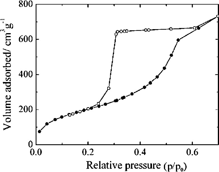
Kr adsorption/desorption isotherm at 77 K on a thin film of dehydrated template-free SBA-15 supported on silicon wafer.
By taking the pore volume calculated from N2 isotherm as reference, one can derive the adsorbed Kr density. It becomes evident that different molar volumes for adsorbed Kr were needed to match the nitrogen and krypton isotherms of powdery mesoporous materials. The values of 35.19, 34.74 and 35.62 ml/mol were found for mesoporous silica MCM-41, MCM-48 and SBA-15, respectively [47]. All the values are smaller than the 36.43 ml/mol reported by Nonaka [53], but greater than the 31.04 ml/mol (2.7 g/cm3) cited by Takei and Chikazkwa [49]. Although the theory/principle used in the surface area and pore size analysis may be fine, the parameters involved in the estimation may warrant further study.
2.2 X-ray reflectivity
Specular XRR (with reflected angle equal to the angle of incident) is a non-destructive technique to measure thin film properties such as film thickness, laterally averaged electron density normal to surface and interfacial roughness [41]. The refractive index of matter in X-ray energy range is n = 1 – δ – iβ, δ = λ2reρe/2π and β = λμi/4π, where re is classical electron radius (re = 2.8 × 10⁻⁶ nm), λ is X-ray wavelength, ρe is electron density of material and μi is linear absorption coefficient of film. Typical value for δ is 10–5–10–6 while β value is 10 times smaller [41]. Since the X-ray refractive index of air is 1 and that of mater is less than 1, when X-ray beam impinging from air to a flat surface with incident angle (θi) below a critical angle θc, it can be totally reflected with
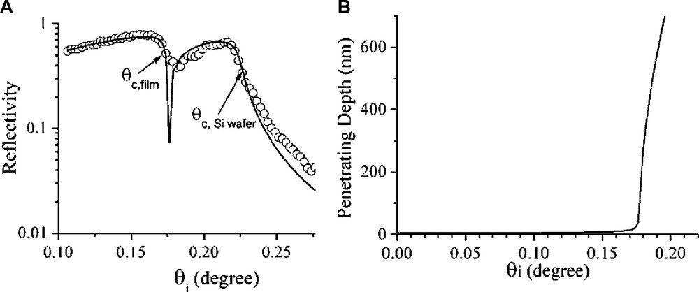
(A) The XRR fitting curve (–) and experimental data (○) of a dip-coated Brij-56 template-free mesoporous film. (B) The plot of calculated penetration depth as a function of incident angle of (A).
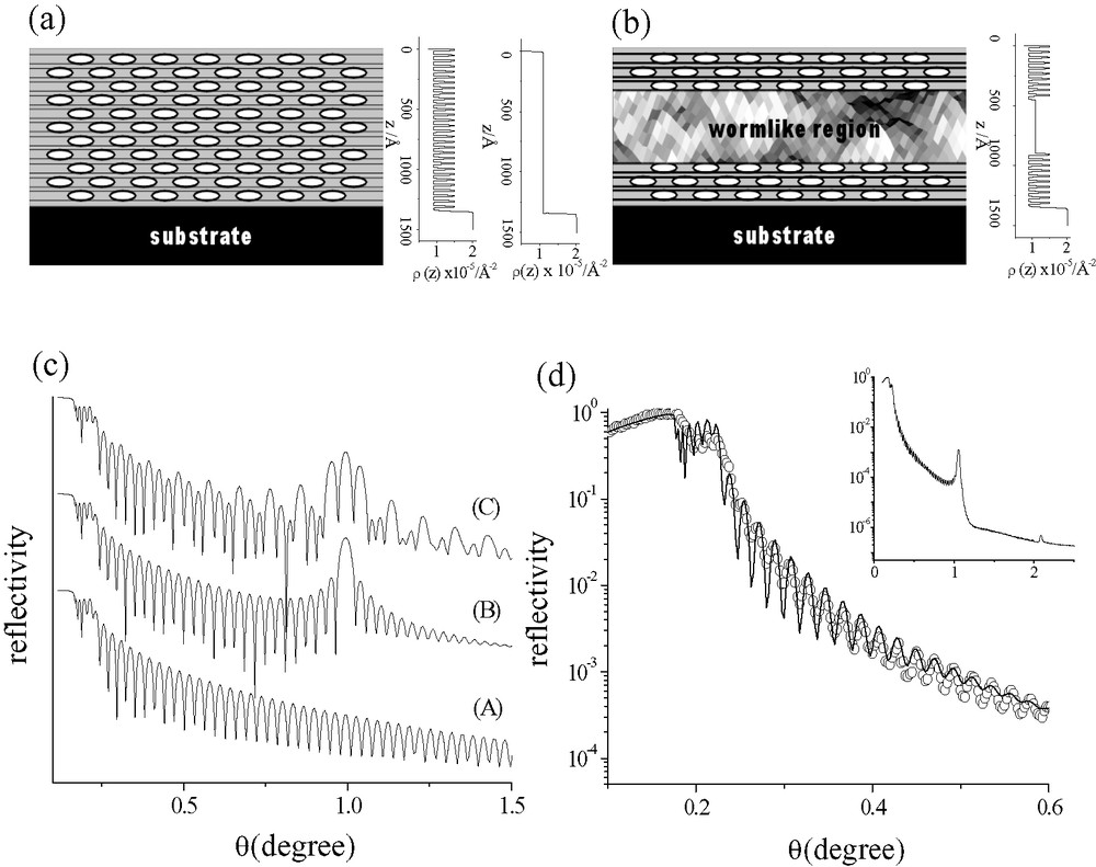
(a) A model of well-organized mesoporous film together with its electron density profiles assuming a series of two alternating layers (multi-layer model) and a model of homogeneous electron density distribution (single layer model) within the film. (b) A model of mesoporous film containing a wormlike region in the center together with its electron density profile assuming a serious of two alternating layers existed near the air-film and substrate–film interfaces. (c) Simulated XRR profiles of (a) by single layer model (A) and by multilayer model (B), and of (b) by multilayer model (C). (d) The XRR experimental data (○) and fit plot (–) of a spin-coated Brij-56 template-free mesoporous film. Simulation of these XRR profile using the Parratt 32 software version 1.5. Masquer
(a) A model of well-organized mesoporous film together with its electron density profiles assuming a series of two alternating layers (multi-layer model) and a model of homogeneous electron density distribution (single layer model) within the film. (b) A model of ... Lire la suite
Densities of nanoporous films are smaller than that of silicon wafer (ρm = 2.3 g/cm3 and ρe = 708.3 e−/nm3), of which the angular position of total reflection critical angle is 0.221° for λ = 0.154 nm. The electron densities of polymethylsilsesquioxane (PMSSQ) films deposited on Si wafer were assumed to be uniform within a film and were observed to be 370–420 e–/nm3, and they are dependent on porosity (0–20%) of films and curing temperatures [56]. Porosity of a film (P) can be derived from the average mass density of film (ρave) and pore wall density (ρwall) as ρave = ρwall (1 – P). Information on PSD was also considered to be derivable through XRR technique by mass uptake of probe molecules and by measuring the total reflection critical angle of thin film before and after exposing it to various partial vapor pressure of a probing molecule, and one such example is toluene for the hydrophobic nanoporous hydrogen silsesquioxane (HSQ) film [57,58]. The critical angle as a function of toluene uptake and the Kelvin equation were used to build the relationship between the pore size and partial pressure of toluene, the PSD could then be calculated.
Doshi et al. [59] found that the as-synthesized form of two-dimensional (2D) hexagonal thin film of cetyltrimethylammonium bromide (CTAB)-templated mesoporous silica (thickness ≅ 586 Å) gave an XRR curve resulting from periodic variation in the derivative of the electron density profile in the z-direction (normal to the Si (100) substrate surface). The presence of oscillation peaks at the high (near the film–substrate interface) and low (near the film–air interface) values of z while with the absence of peaks at intermediate values indicates the existence of a disordered region sandwiched between ordered regions at the substrate–film and film–air interfaces in the thin film. All these confirm the interfacial growth of the mesoporous film.
The as-synthesized form of free-standing film of CTAB-templated mesoporous silica grown on air/water interface consists of 21 layers as examined by XRR [60] and analyzed by a slab model. Which could approximately be separated into a series of two alternating layers: one corresponds to organic surfactant micelle in the cylindrical channel of layer thickness ≅ 3 nm and ρz ≅ 9 × 10⁻⁴ nm–2 and the other is associated with a low density silica phase of layer thickness ≅ 1.5 nm and ρz ≅ 10.5 × 10⁻⁴ nm–2 (where ρz is electron density per area); similar to the model in Fig. 3a.
The densities of P123 (H(OCH2CH2)20(OCH2CH2CH2)70(OCH2CH2)20OH block copolymer)-template-free mesoporous silica films deposited on Si (100) wafer were recently found by us to be lower than that of Brij-56 (C16H33(OCH2CH2)10OH)-template-free films [61]. It was also noted that the XRR densities of these mesoporous films were sensitive to the water uptake due to the existence of hydrophilic Si–OH groups on the intrachannel surface. Thickness of P123 and Brij-56 template-free films was analyzed by the Kiessig fringes of XRR curves with a single layer model. Both the single layer model [55,61] and the multi-layer model [60] can be applied for a well-organized film with uniform pore packing arrangement throughout the film. The same frequency values of Kiessig fringes are obtained as shown in Fig. 3c. However, for the multi-layer model consisted of a series of two alternating layers, there are out of plane diffraction peaks on top of the oscillations of Kiessing fringes (profile B of Fig. 3c).
Another example of mesoporous film XRR profile fitted by single layer model is the CTAB or P123-templated mesoporous silica and alumina thin film prepared by Klotz et al. [62]. From the average mass density (ρave) and the pore wall density (ρwall, 2.00 g/cm3) by pycnometry, they evaluated the porosity of mesoporous film according to the equation ρave = ρwall (1 – P). The porosity derived from the XRR and pycnometer corresponds well with the porosity determined by nitrogen adsorption–desorption measurement.
Wall thickness and core radius of dip-coated CTAB-templated mesostructure silica film were measured by Gibaud et al. [63]. Through the combination of XRR and GIXD measurements, invaluable information such as the radius of the cylindrical rods and the distance between their cores of as-synthesized thin film of CTAB surfactant-templated 2D hexagonal mesoporous silica could be obtained. It has recently been demonstrated that the structural and physical properties of porous thin films deposited on silicon wafer up to 1.4 μm thick can be accurately characterized by high resolution specular XRR and small-angle neutron scattering [64].
In addition to specular reflectivity, there is an off specular characterization (reflected angle does not equal to the angle of incident): Brennan et al. [65] investigated the growth of silica-surfactant mesostructured film at the air/water interface using diffuse XRR technique. The changes of peak intensities of specular reflectivity and Yoneda wing with various CTABr/TMOS ratios and induction period were monitored to study the growth of CTAB-mesostructure films at the air/water interface.
XRR technique has been widely used in organosilane nanoporous films such as hydrogensilsesquioane (HSQ) and methylsilsesquioane (MSQ) to derive their film properties. [66,67] The XRR profiles of these nanoporous films were found to be similar to those of mesoporous films except the existence of Bragg peaks from the ordered pore arrangement of mesoporous films. Film properties such as porosity and pore wall density can thus be obtained.
2.3 Grazing incident X-ray diffraction
Reflection mode XRD, i.e. the θ – 2θ conventional XRD, is well-established for the characterization and the identification of structures of powdery mesoporous samples. However, the bundles of channels in mesoporous silica films are usually expected to pack and align themselves in a specific and preferred orientation at air–solution interface or on a flat substrate. With such ordering of pores, only lattice planes parallel to the surface, d//s, can be detected by XRD patterns in θ – 2θ scan mode as shown in Fig. 4a [68]. To acquire information more than out-of-plane periodic lattice in the film, GIXD technique is employed (Figs. 4 and 5). Using GIXD technique, incident angle of X-ray (θi) should be set at a very small-angle, usually at the critical angle of total reflection (θi = θc) and the incident beam will be reflected in the direction having (90°– θi) angle with the normal to the surface in a specular geometry. For θis that are slightly higher than θc, the incident beam will penetrate into the film (Fig. 2b) and be diffracted along β axis if some periodicities normal to the film are in agreement with Bragg’s law (Fig. 4b). If a thin-film sample was aligned precisely parallel to incident X-ray beam at θ = 0° and θi could be set around θc, 2θ should then be set equal to twice that of θi in order to get higher reflected intensity during in-plane measurement. Normal axis of the thin film, α, and in-plane angle of the detector, β, together with the geometry of the in-plane diffraction are given in Fig. 4c. The d-spacings of periodicities normal to the surface, d⊥s, can be obtained from in-plane XRD by nλ = 2 d sin(β/2). Furthermore, after the in-plane structural information is retrieved, the detector can be fixed at certain in-plane XRD peak position and let the sample rotate around the α-axis to obtain the direction distribution of grains in in-plane direction. Nevertheless, information from conventional or out-of-plane and in-plane XRD patterns give d-spacings of periodicity parallel (d//) and normal to the film (d⊥), respectively. To resolve the texture of the film, a 2D detector instead of a point detector is recommended for GIXD. An X-ray sensitive imaging plate or charge-coupled device (CCD) camera is used in a 2D GIXD experiment as illustrated in Fig. 4c [69,70]. Due to the absorption of substrate, only half of the diffraction data can be collected for a thin film deposited on a thick substrate. However, either a thin self-supported film [69] or a sample of very thin substrate [70], whole diffraction pattern can be collected. 2D GIXD patterns (Fig. 5) provide the structural information about both out-of-plane and in-plane lattices, as well as periodicities that are neither normal nor parallel to the film surface. By using real time detection through CCD camera and with a synchrotron X-ray source, in situ experiments can also be performed in a time scale less than 1 s [71].

Schematic representations of (a) conventional out-of-plane θ – 2θ mode XRD, the detector scans in the plane perpendicular to the film surface; and (b) grazing incident in-plane mode XRD, incident beam and outgoing beam parallel to the film surface with β angle. θi is often set at θc (c). An illustration of geometry used for 2D GIXD measurements; a beamstopper is usually used to shield the direct beam and total reflection beam in order to avoid signal saturation of imaging plate, the 2D detector; the beams i, r, and d represent the incident, reflected and in-plane diffracted X-ray. The point detector can scan in either vertically (2θ) or horizontally (β). Masquer
Schematic representations of (a) conventional out-of-plane θ – 2θ mode XRD, the detector scans in the plane perpendicular to the film surface; and (b) grazing incident in-plane mode XRD, incident beam and outgoing beam parallel to the film surface with ... Lire la suite
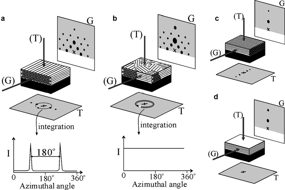
Illustrations of 2D transmission and GIXD patterns thin films in p6mm hexagonal symmetry (a–c) and lamellar structure (d). The XRD patterns are collected on a well-aligned single-crystal like hexagonal structure with grazing incident X-ray parallel (a) and normal (c) to the channel direction. The GIXD pattern of a polycrystalline mesoporous silica film with a preferred orientation axis normal to substrate surface (b). Of which the transmission XRD pattern shows rings (b) instead of spots (a) and (c). The scattering intensity of transmission XRD patterns can be integrated along the azimuthal axis as indicated by the dash arrows in (a) and (b). The integrated patterns can be used for determining the orientation distribution of mesopores. The transmission XRD pattern of lamellar thin film (d) show no diffraction peaks. The letters ‘G’and ‘T’ indicate the X-ray sources (in parentheses) and the corresponding XRD patterns for grazing incident and transmission measurements, respectively. Masquer
Illustrations of 2D transmission and GIXD patterns thin films in p6mm hexagonal symmetry (a–c) and lamellar structure (d). The XRD patterns are collected on a well-aligned single-crystal like hexagonal structure with grazing incident X-ray parallel (a) and normal ... Lire la suite
Combining with GIXD and transmission mode XRD technique (Fig. 5) to analyze a mesoporous silica thin film dip-coated on a very thin substrate (10-mm thick Si wafer) [69], it was found that even the 2D planar unit cells were well aligned perpendicular to the surface of dip-coated samples, but the channel axes were still found to be randomly orientated within the plane parallel to the surface.
Miyata and Kuroda [31] found that the channels of mesoporous silica films with thickness less than 0.3 μm were aligned well in perpendicular direction to the rubbing-treated flat glass substrate and thus presenting a 2D hexagonal columnar structure. In this case, only (h00) reflections, i.e. (100), (200) etc. were observed by conventional out-of-plane XRD. The axial preferred orientation of the mesochannels was confirmed by the narrow full width at half maximum (FWHM of diffraction peak) values of the diffraction intensity with α-scan of the in-plane XRD.
Besson et al. recorded GIXD patterns at different incident angles for films derived from silica sols with different period of aging. Interior of the film was found to be organized with the presence of Bragg spots after the growth of ordered domains at the air–sol interface. They suggested that the growth of mesoporous film starts from the nuclei at the liquid–vapor interface [72].
A time-resolved GIXD was also used to study the very fast self-assembly process during film formation [73]. Time scale of the in situ GIXD experiments is less than 1 s and is considered suitable for investigating the growth of mesostructure in a dip-coated film under a controlled atmosphere. Gibaud et al., Grosso et al. and Chao et al. suggested [34,73–75] that the solvent evaporation rate could be controlled by environment and is also important for the formation of the final mesostructure.
The diffraction patterns of GIXD provide the bulk average information about lattice parameters of 2D structures in thin films, while the uniformity over the film thickness and the texture of film relative to the substrate were also viewed by the cross-sectional TEM and electron diffraction (ED) measurements by us [75]. The continuous mesoporous silica film deposited on silicon (100) wafer of 0.2 μm thickness was prepared by dip-coating of Brij-56 templated precursor and then calcined to 500 °C. The texture of template-free film was investigated by the cross-sectional TEM and GIXD and was found to have well-organized pore arrangement throughout the film. However, the directional distribution of bundles of mesochannels in the film as observed by both transmission mode XRD and top-view TEM revealed no preferred in-plane orientation [75], and this is similar to the structure of hexagonal mesophase silica films dip-coated on silica glass and silicon wafer substrates using F127 (OH(CH2CH2O)106 (CHCH3CH2O)70 (CH2CH2O)106H, Pluronic block polymer) templated silica sol [70]. The results of both studies [70,75] suggested that even the structure of mesoporous silica and grain growth in a film could be direction-dependent, and the preferential ordering normal to the substrate could be disturbed by the deposition of precursor-sol grains on the substrate during the initial stage of coating process.
2.4 Transmission electron microscopy
TEM technique is usually conducted with ED or Fourier transformation (FT) calculation simulation for a direct view of pore structures of mesoporous materials. For those who are interested in observing preferred orientation of mesoporous grain to the substrate and the pore morphology of mesochannels affected by substrate and anisotropic shrinkage from heat treatment [70], thin film specimen should always be together with its host substrate. To prepare ‘on-substrate’ thin film specimens for cross-sectional TEM characterization, a sample can first be cleaved into small pieces, and two pieces can be glued together through face-to-face contact. The glued stacks are then ground, polished and milled. At the thin section of a TEM specimen containing the interface of mesoporous silica and substrate, electron transparency can be achieved. A top-view TEM can also be examined using on-substrate sample, which, in turn, has been polished to achieve good electron transparency. It is to be noted that TEM result is localized; therefore, it is desirable to further examine its consistency with XRD investigation.
3 Application
With the confinement of intramesochannel void and easily functionalized channel surface, the applications of mesoporous film have been demonstrated to expand from catalysis and separation, similar to zeolites but with large pore sizes to be accessed by bulk molecules, to electronic and optical fields. In this section, selected applications of mesoporous films and functionalized mesoporous films on optical and electronic applications are highlighted.
3.1 Low-k dielectric
As integrated circuit (IC) technology rapidly advances towards sub-100 nm nodes, ultra-low dielectric constant (k) materials are badly needed to minimize RC delay, signal cross-talk and power dissipation in ULSI devices [76]. Over the past few years, tremendous research on those new interlayer dielectrics (ILD) have been performed in order to replace the conventional Al(Cu)/SiO2 metallization. Reduction of the k value of ILD relative to SiO2 (k = 4.0) can be achieved by lowering density and polarizability of materials [36,77]. High electronegativity of F atom reduces the polarizability of C–F bonds. While the density of dielectric materials can be lowered by incorporating either lighter atoms or more void space for air (k = 1). Two types of films have been developed for low-k application, one is the composites of SiO2-based materials of k = 1.3–3.5, such as SiO2Fy, HSQ, MSQ, mesoporous organosilicas, porous silica, nanoporous silica in aerogel/xerogel, porous silicas with porogens, and molecularly templated mesoporous silica; and the other is the C-based materials of k = 1.9–3.6, such as polytetrafluoethylene (PTFE), F-doped polyimides, poly (aryl ether) and nanofoams. Among the various low-k dielectrics, nanoporous silica materials are widely believed to be the most promising ILD material for sub-100 nm technology nodes because of their tunable ultra-low k value and their similar chemical composition as the conventional SiO2 dielectric [22]. Besides, porous silica films have high thermal stability and are compatible with silicon wafer and related materials in the existing IC technology [23,78,79].
Due to its high porosity and channel microstructure, calcined spin-on mesoporous silica films are generally hydrophilic and, therefore, have very poor stability in dielectric properties. Trimethylsilylation by hexamethyldisilazane (HMDS) vapor post-treatment and trimethylchlorosilane (TMCS) mixed with the organic-templated silica sol precursor were adopted to improve the hydrophobicity and thus to stabilize the dielectric properties of the nanoporous silica films [80,23]. Ultralow dielectric constants of 1.4–2.5 were obtained on spin-on hydrophobic mesoporous silica films. Of which the hydrophobic property was found to be thermally stable at temperatures as high as 400–500 °C by thermal desorption mass spectrometry. Trimethylsilyl groups (–Si(CH3)3) bonded on the intrapore surface of the mesoporous silica film is susceptible to degradation upon exposing to reactive plasmas used for capping, etching, and ashing processes. Plasma can induce chemical modifications in the film, causing film densification, and formation of dangling bonds and defects. All of these can increase the k-value or cause other integration problems. Patterned nanoporous silica films by reactive ion etching were prepared, and a combination of post-annealing, hydrogen plasma treatment, and HMDS vapor treatment was found to be effective to alleviate damages caused by dry etching. The structure of nanoporous silica films was detected by X-ray diffraction and was found to be well in order even after the dry etching process, this suggests that the nanoporous silica can withstand the plasma dry etching [81,82].
Mechanical strength of porous films is expected to be weaker than their fully dense analogues. Low-k porous materials with low mechanical properties will have difficulties to endure integrating cycles such as chemical, mechanical polishing (CMP), dry etching, and packaging processes. Such porous materials as ILD candidates for IC process will constantly face the trade-off in dielectric constant and mechanical properties. Porosity, pore structure and intrapore surface properties of a porous material have all been found to affect the dielectric constant of thin silica film as well as its mechanical strength [37,80].
It is reported that the Cu/low-k interconnect integration has some integration problems in thermal copper diffusion and agglomeration of narrow Cu interconnect at high temperature, so, its processing temperature should be kept low. The application of low temperature photocalcination [83], O2-plasma [84] and ozone ashing [37,85] treatments in contrast to the conventional thermal calcination were thus studied during the removal of organic templates.
3.2 Photoluminescence
Although bulk silicon is extremely inefficient at emitting light, silicon nanocrystals and highly porous silicon can emit red, green and even weak blue light when stimulated by light of shorter wavelength [86]. Since silicon nanocrystals have energy bandgaps wide enough to produce visible light (2–3 eV) than the 1 eV in bulk silicon. Many efforts have thus been devoted to exploit Si-related light sources including Si/SiO2 superlattice [87] and Si clusters in mesoporous SiO2 film [88]. The silicon clusters of ~1 nm size in orientated hexagonal mesoporous silica film displayed yellow–orange photoluminescence (PL) with a UV excitation at 308 nm.
The nature and the role in PL of walls among pores in mesoporous SiO2 materials were studied recently [89,90]. The PL from mesoporous silica with the pore size of ~6 nm and the thickness of wall among pores of ~1 nm was induced by Nd:YAG laser at λ = 266, 354.7 or 532 nm and observed at room temperature [89]. Since bulk SiO2 is a wide band gap insulator (the band gap of bulk silica Eg ≅ 11 eV), it was suggested that PL has been derived from a direct one-photon excitation of hydrogen-related species and non-bridging oxygen hole centers on the pore wall of mesoporous silica. PL induced by ultraviolet (UV) or vacuum UV light of mesoporous SiO2 may be similar to that of surface-oxidized nanocrystals and porous silicon.
3.3 Other applications
The semiconducting polymer, poly [2-methoxy-5(2′-ethyl-hexyloxy)-1, 4-phonylene vinylene] (MEH-PPV) was incorporated in aligned mesochannels of a mesoporous film prepared by the rubbing polyimide method [31] and it showed highly polarized luminescence [91]. Highly aligned mesoporous silica films filled with guest conducting polymers that are intrinsically anisotropic in their intramolecular conductance and luminescence polarization may have potential for photonic applications and other optical applications [92], as they are optically clear and can emit polarized light.
The mesochannels of thin films are easily accessible by the external environment and increases the performances for sensing applications. Electrical current variation with relative humidity was observed on template-free mesoporous films [18]. In addition, mesoporous film loaded with Pt/Pd can act as efficient filter to improve the selectivity and stability of SnO2-based gas sensors [19]. Mesoporous film was used as a pH-sensor, by incorporating pH-sensitive dye [20] and was integrated into the surface photovoltage gas sensing system for NO detection [21], as well as coated for anti-reflection of light [39].
4 Summary
In this report thin film X-ray methods, including reflectivity and diffraction, have been demonstrated as powerful tools in analyzing structure and pore properties of mesoporous thin films and in monitoring the formation of mesoporous thin films. Pore properties such as surface area, pore volume and PSD can be cross-checked against that extracted from traditional physisorption of Kr. Conventional structural investigations such as TEM and ED are used to study the pore structure and film texture as well as to confirm the findings from GIXD and XRR. With the availability of X-ray sources from synchrotron radiation of high photon flux and significant improvement of computers and detecting devices, thin film X-ray techniques have generated significant impact on current mesoporous thin film research. The development of on-substrate characterization techniques will be a big plus in correlating the information from mesoporous thin films with their applications.