

1 Introduction
The success of CuInS2 (CIS) as a large-scale applicable absorber material for solar cells depends crucially on the replacement of the KCN etch by a less toxic and ecologically acceptable procedure: during initial preparation of the CIS films by sequential Cu and In sputtering and subsequent annealing in S atmosphere [1], the Cu/In ration is kept Cu rich in order to achieve a good crystal growth. However, for Cu-rich CIS, the Fermi level is known to be very close to the valence band edge which makes the material a p+ -type semiconductor [2] and unsuitable as absorber. Fortunately, the bulk composition self-adjusts to stoichiometry during the annealing step which leads to a segregation of the excess Cu as sulphidic phases on the surface and along grain boundaries [3,4]. The KCN treatment is used to selectively remove these copper sulphides from the CIS surface [5,6]. During the etch, Cu(I) and Cu(II) sulphides dissolve, forming Cu cyanides and Cu cyanocuprates [7].
To avoid the use of KCN, investigations have been carried out on electrochemical conditioning procedures for the removal of the copper sulphides [8]. In the past, simple cathodic and treatments in K2SO4 supporting electrolyte [9,10] and anodic treatments in V2+/V3+ redox electrolyte solutions yielded absorber layers that showed efficiencies of 1.3% in PECS [11] and no noticeable efficiencies in solid-state solar cells. Based on these results we developed a more complex conditioning protocol, which is based on multiple potential-scan-hold subprocedures in a V2+/V3+ electrolyte solution [12,13]. Actually, the whole procedure consists of two treatment stages: at first, the predominant covellite, CuS is dissolved at anodic potentials below 0.5 V against the saturated calomel electrode (SCE). In the second stage, potentials above 0.6 V (SCE) are being employed to dissolve a small sacrificial layer of CIS thereby removing remnant copper sulphides such as chalcocite, Cu2S.
2 Experimental
The CIS samples were received from HMI baseline production where they had been prepared as described elsewhere [1].
2.1 Treatment in vanadium and PECS operation
For the electrochemical experiments in V2+/V3+ solutions a potentiostat PG285 (HEKA Elektronik, Lamprecht, Germany) was used in a standard 3-electrode set-up with a SCE as reference (all electrochemical potentials are given with respect to the SCE) and a graphite rod as counter electrode. The samples were illuminated during the treatment and the PECS operation (except when recording the dark current characteristics) by a W–I halogen lamp with a total power density of 54 mW cm−2 at the sample. This set-up was also used for the PECS measurements. The 0.4 M V2+/V3+ in 3.5 M HCl electrolyte solution was prepared as described elsewhere [14], brought to a redox potential of –0.45 to –0.46 V by addition of Zn and constantly purged with N2, purity 99.999% (Messer Griesheim, Krefeld, Germany). The same solution was used for treatment and PECS operation.
2.2 Treatment in EDTA containing electrolyte
The experiments involving the EDTA were performed using a potentiostat Wenking PGS81R (Bank Elektronik, Clausthal-Zellerfeld, Germany) with a SCE as reference and a platinum sheet as counter electrode. During the treatment, the samples were illuminated using a 20-W W-I halogen lamp. The electrolyte was a stirred mixture of 40 ml H2O, 1 ml 85% H3PO4, 0.5 g EDTA and 0.5 g Zn.
Solutions were prepared using deionised water (R = 18 MΩ cm, TOC 3–5 ppb). CHCl3, CH3OH, HCl (37%), H3PO4 (85%) were of analytical grade and supplied by Merck (Darmstadt, Germany). EDTA (99.4%), KCN (96%), V2O5 (99.8%) and Zn (99.8%, –20 mesh) were obtained from Alfa Aesar (Karlsruhe, Germany). All chemicals were used as received.
2.3 Non-electrochemical film characterisation
The solid-state device measurements were performed using an AM 1.5 solar simulator with a light intensity of 100 mW cm−2. For the X-ray photoelectron spectroscopy (XPS) measurements, a commercial system (SPECS GmbH, Berlin, Germany) with a PHOIBOS analyser was used. The excitation energy was 1253.6 eV (Mg Kα radiation). The base pressure in the analysis chamber was below 10−10 hPa. Before measuring the samples were rinsed thoroughly with water, methanol and chloroform and dried in a N2 stream.
3 Results and discussion
The choice of the potential limits is illustrated in Fig. 1, which shows a cyclic voltammogram (CV) of an as grown CIS layer in an acidic V2+/V3+ electrolyte. Starting at –0.3 V, the onset of a current can be observed, which reaches a plateau at –0.05 V. This current results from the mass transport limited oxidation of V2+. Between 0.1 and 0.2 V, some small oxidation peaks occur, which we can not, at the moment, assign to distinct chemical reactions. The predominant features are a double peak structure at 0.4 and 0.5 V (marked by the two arrows pointing upwards) resulting from the dissolution of CuS and the thermodynamically more stable Cu2S, respectively, and the decomposition of CIS at potentials > 0.6 V (marked by the downward arrow) [15].
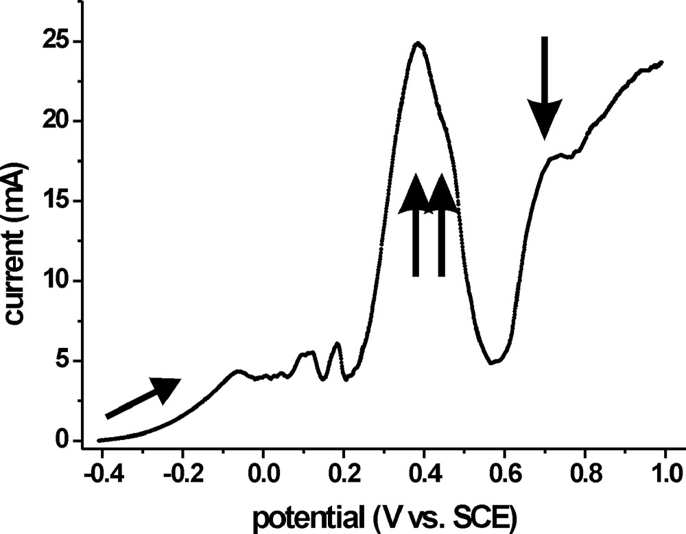
Cyclic voltammogram of an as grown CIS film (sample area: 0.5 cm2) in 0.4 M V2+/V3+ electrolyte; the double peak structure at 0.31 and 0.39 V (upward arrows) can be attributed to dissolution of CuS and Cu2S, respectively, whereas the current at E > 0.6 V (downward arrows) results from CIS dissolution. The scan speed was 10 mV s−1, starting point and initial direction are marked by an arrow.
To avoid the use of the destructive potential region we are also investigating combined electrochemical/chemical conditioning methods. This approach utilises chemical complex formation using EDTA as a model complexing agent [16]. In addition to stabilising the Cu2+ ions in the solution, the presence of EDTA in an electrolyte solution during electrochemical conditioning can be expected to facilitate the dissolution by specific adsorption of EDTA to the CuxS and weakening of the back-bonds of the affected Cu atoms.
For the electrochemical treatment of CIS films in V2+/3+ solution, a two stage procedure gave the best results. The potential profile for stage 1 is shown in Fig. 2: it starts with a cyclic voltammogram from open-circuit potential (OCP) at t = 0 (OCP0, usually –0.2 V) to the solution potential (Esol, usually –0.455 V), to 0.15 V and back to OCP0 for characterisation of the unmodified film under PECS conditions. This is followed by 5–8 reiterations of a scan-hold-scan-hold subunit: The potential is scanned from OCP0 to 0.45 V, where CuS is supposed to decompose, held there for 50 s to allow for off-diffusion of Cu2+, scanned back to OCP0 and held for 50 s to reactivate the surface. The final part of stage 1 consists of 5 cycles in the range Esol to 0.15 V to evaluate the film behaviour during PECS operation.
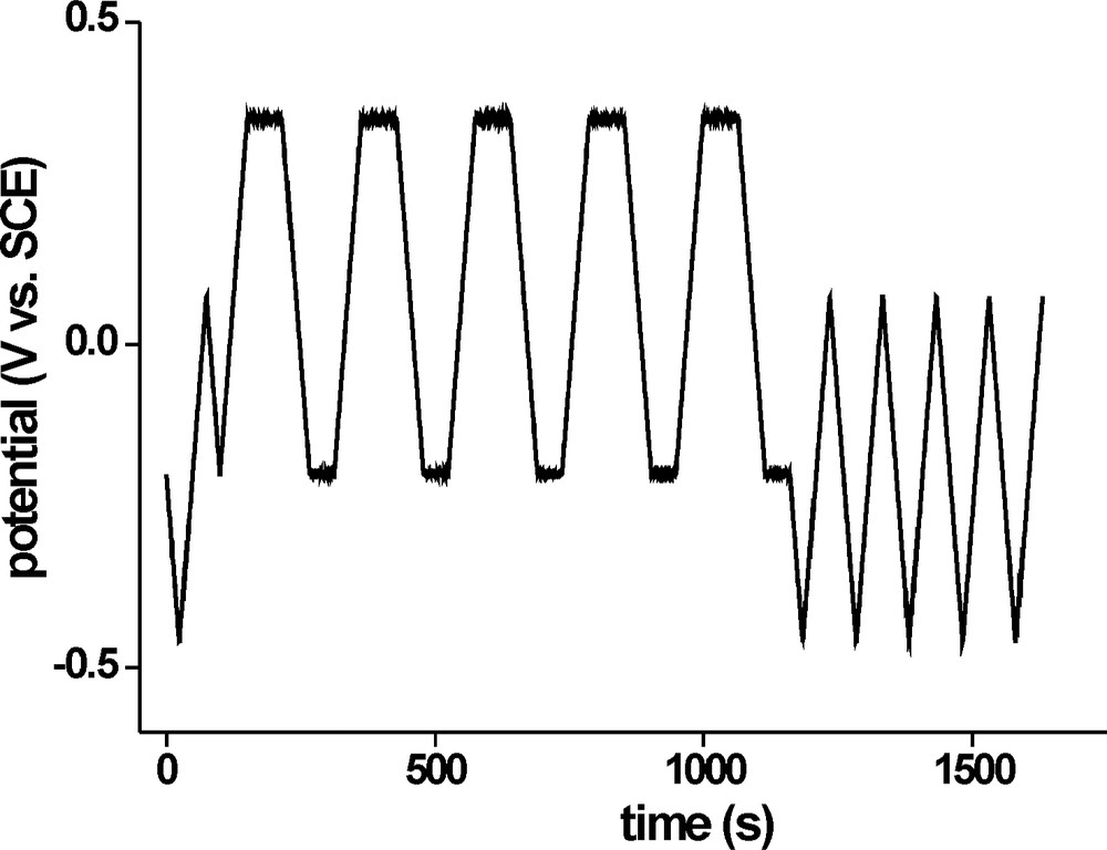
Potential profile for the first treatment stage (V2+/3+); after an initial characterisation by cyclic voltammetry, the sample undergoes several repetitions of a scan-hold procedure followed by PECS operation.
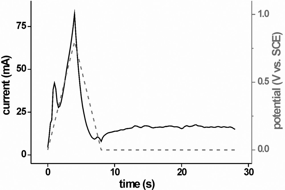
The current response during the first scan-hold-scan-hold subunit is shown in Fig. 3: With the increase of the potential from OCP0 the onset of an anodic current can be observed which passes into a current plateau of I ≈ 20 mA due to mass transport limitation. At E ≈ 0.24 V, a distinct double-peak structure appears, which shows a transient behaviour when the potential is held at 0.45 V. This indicates the dissolution of CuS and the associated passivation of the surface. After 20 s at 0.45 V, the current goes down to 20 mA, which results from the mass transport limited oxidation of V2+. When the potential is scanned back to OCP0, a depression in the current plateau can be observed with a local minimum at 0.25 V. This may be attributed to readsorption of Cu due to incomplete off-diffusion of the Cu2+ ions. Finally, when OCP0 is reached and the potential is being held there, a small but increasing cathodic current is measured. This is in fact a photocurrent and indicates the improvement of the absorber quality of the sample. With an increasing number of repetitions of this subunit, the dissolution peak reappears, indicating a reactivation of the surface during the OCP0 period, but diminishes from each time until after five to eight cycles it is no longer visible. The readsorption feature during the backscan also abates with each consecutive scan and the photocurrent increases. The PECS operation at the end of stage 1 usually yields efficiencies of 2.8% and solid state cells produced from films at this stage yield up to 4% efficiency. XPS measurements show that the surface is still Cu rich and X-ray emission spectra (XES) which will be the topic of a forthcoming publication, indicate the nature of the remaining Cu species to be mainly Cu2S.
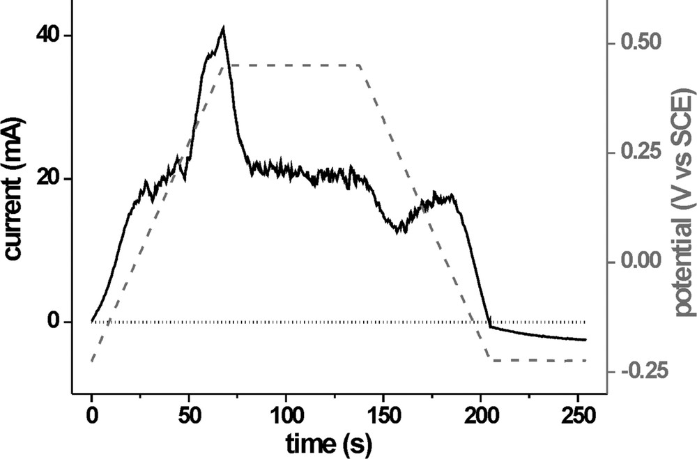
Current response (solid black line) of a CIS sample (sample area 0.5 cm2) during the first scan-hold sequence (V2+/3+), the potential profile is indicated by the dashed grey line and I = 0 by the dotted black line.
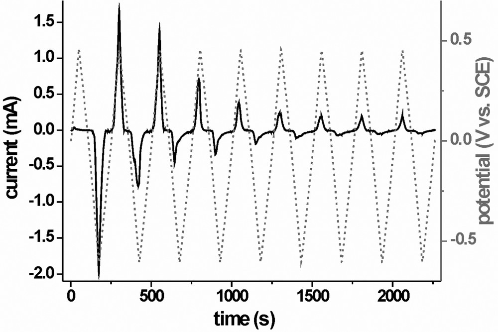
To dispose of these copper sulphide remnants, we designed the second stage of the conditioning procedure. It makes use of a potential range up to 0.8 V and dissolves a small sacrificial layer of CIS to remove Cu sulphides which are thermodynamically more stable than covellite or located in grain boundaries and hardly accessible to the electrolyte solution. Fig. 4 shows the potential profile for this second stage: The important subunit is a potential cycle from 0 to 0.8 V and back to 0 V again, at a speed of 200 mV s−1, followed by 20 s at 0 V for off-diffusion of products and surface reactivation. The purpose of the high scanning speed is to limit the time during which the sample is being kept at destructive potentials. It is, however, not advisable to apply rectangular potential pulses of 0.8 V to the film because the electromechanical strain tends to cause the whole CIS layer to come off in flakes. The subunit is usually run through three to five times. After that, the potential is slowly scanned to +0.45 V where it is kept for 120–180 s. Finally, as with stage 1, PECS operation for performance evaluation concludes the second treatment stage. The current response of the first run of the subunit is shown in Fig. 5. With the start of the potential scan we see an immediate current increase with a local maximum at E ≈ 0.22 V. This may be attributed to dissolution of copper sulphides and also because of the high scanning speed it is very pronounced.
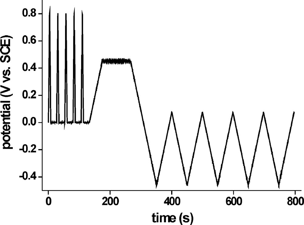
Potential profile for the second treatment stage (V2+/3+) consisting of five reiterations of the fast destructive potential scan and finally the evaluation of the cell performance during PECS operation.
Current response (solid black line) of a CIS sample (sample area 0.5 cm2) during the first scan-hold sequence of the second treatment stage (V2+/3+), the potential profile is indicated by the dashed grey line.
The current plateau due to mass transport limited oxidation of V2+ is not visible in this region because this part of the curve is dominated by capacitive currents. As the potential reaches its maximum of 0.8 V, so does the current which quickly drops again when the potential is scanned back. At E ≈ 0.25 V a small depression can be observed in the current which is clearly distinguishable from the capacitive global minimum at the point where E reaches 0 V again. This depression may be attributed to Cu readsorption caused by incomplete off-diffusion of Cu2+ ions. During the 20-s hold period (sample at 0 V) the capacitive current decreases quickly and a constant anodic current flows, resulting from the oxidation of V2+. When the subunit is repeated, the features at 0.25 V in the forward- and back scan diminish very quickly and are no longer observable after three to five runs. At this point the potential is slowly (10–20 mV s−1) scanned to 0.45 V and kept for 2–3 min. During this time, the mass transport limited anodic current can be measured. The second treatment stage is finally concluded by running five cycles to evaluate the PECS performance of the film. Efficiencies of 3.3% are achieved and solid state devices yield 8%.
The potential protocols we are currently investigating for the combined electrochemical–chemical conditioning in EDTA containing electrolytes are much simpler and consist of multiple repetitions of a cyclic voltammogram in the range between –0.6 and 0.45 V. The potential profile and current response for a typical experiment are depicted in Fig. 6. In the first anodic scan, almost no current response can be seen from the sample. Only after a cathodic ‘activation’ scan down to –0.6 V, a strong oxidation current is visible in the second anodic scan. Supplementary experiments have shown that this cathodic activation scan has to go to potentials lower than –0.55 V to result in a notable oxidative current response in the following anodic scan. In successive potential cycles both the anodic and cathodic features diminish until after seven to eight total cycles a constant current response is attained. With the H3PO4 containing electrolyte, a photoeffect, probably the reduction of PO43– to PO33– by photogenerated electrons, can be observed, but the current is potential dependent and the system can not be operated as a PECS. For the evaluation of the efficiencies, the samples are transferred to the vanadium set-up. After this conditioning, conversion efficiencies are at 1–2%, the sample whose treatment is presented here yielded 1.44% (cf. the I/V characteristic in Fig. 7c). Solid-state devices have yet to be fabricated and tested. Also, the role of the Zn is not yet fully clear and further investigations on this are in progress.
Potential profile (dashed grey line) and current response (solid black line) for the electrochemical conditioning of an as grown CIS sample (sample area: 0.17 cm2) in EDTA containing electrolyte mixture.

I/V characteristics of solar cells built from differently treated CIS films; (a) solid-state cell after two-step electrochemical (V2+/3+) treatment (η = 7.25%), (b) PECS after two-step electrochemical (V2+/3+) treatment (η = 3.3%), (c) PECS after combined ec/c conditioning using EDTA (η = 1.44%).
I/V characteristics of solar cells made from differently treated films are shown in Fig. 7. The curve 7a results from a solar simulator measurement of a solid state cell after both stages of the electrochemical (V2+/3+) treatment, yielding 7.25% efficiency, 7b is a PECS characteristic of a two stage electrochemically conditioned film (η = 3.3%) and 7c is the PECS performance of the sample whose ec/c treatment (EDTA) is discussed above (η = 1.44%). The potentials of the PECS curves are given with respect to the redox potential of the electrolyte solution and not vs. SCE. The slight upward bend of curve 7c at results from hydrogen evolution at the sample and superimposed to the V3+ reduction or a corrosion reaction on fresh samples observed earlier [17].
Over time, the pH of the V2+/3+ solution increases because Zn is added for the potential adjustment and the Zn reduces not only V3+ but also protons, forming H2 and decreasing the H+ concentration. This has at least twofold consequences: first, the competing reduction will be in favour towards the vanadium reaction and secondly, the surface condition of the semiconductor can be altered at increased pH.
From comparison of the curves, it is clearly visible that the photovoltage of the chemically–electrochemically (EDTA) treated sample, 7c, is 0.128 V lower than that of the electrochemically (V2+/3+) treated one, 7b, which hints at a still incomplete removal of copper sulphides by this treatment. This assumption is corroborated by XPS investigations of the differently treated surfaces. Fig. 8 shows the Cu 2p3/2 and In 3d5/2 core level region, individually normalised for each sample. By integration of the curves and multiplication with the atomic sensitivity factors, the Cu/In ratios X for the different samples can be calculated. For the as grown sample, curve 8a, the surface is Cu rich (X = 8.58). The KCN etched reference sample, 8b (the curve is drawn in grey because it intersects with 8a), is Cu poor with X = 0.32, whereas the electrochemically (V2+/3+) treated surface is almost stoichiometric (curve 8c, X = 0.68). After the combined chemical–electrochemical (EDTA) conditioning the surface still remains Cu rich (curve 8 d, X = 1.31).
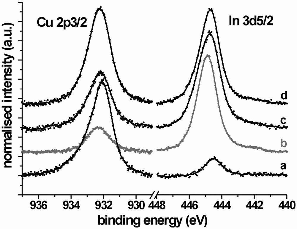
XP spectra (Mg Kα) of CIS samples after different treatments; (a) as grown, (b) KCN etched, (c) after two-step electrochemical (V2+/3+) conditioning, (d) after electrochemical/chemical conditioning in the presence of EDTA.
4 Conclusions and outlook
Our investigations on replacing the toxic KCN etching by an electrochemical procedure yielded an electrochemical conditioning method using a V2+/V3+ which produces comparable and only slightly inferior results. One challenge for the further optimisation is the mass transport during the treatment, i.e. the prevention of readsorption of Cu2+ ions which would drastically reduce the treatment time. Our new approach to combine chemical and electrochemical treatment in a way that the free reaction energy of the chemical reaction reduces the electrochemical potentials needed for the dissolution also shows promising results. Here, we still work with simple potential protocols which leave much room for improvement and already receive measurable efficiencies in PECS. Furthermore, mass transport seems not to be a problem as we cannot detect any features in our electrochemical measurement curves which indicate readsorption. The main problem for this method may be Cu–S-phases located in grain boundaries or otherwise inaccessible for the electrolyte. Furthermore, EDTA is also an ecologically questionable substance, but we use it as a cheap and well-known model system and plan to replace it later. Preliminary experiments with biodegradable complexation agents were very encouraging.
Acknowledgements
The authors are grateful for the CIS samples provided by J. Klaer, HMI, the preparation of the solid state devices done by C. Kelch, HMI and the XES measurements done by the CISSY group at BESSY II.