

1 Introduction
Feature miniaturization on Si surfaces has various application routes. Among those, the fabrication of photonic band gap (PBG) materials with a shift of the photonic gap towards the visible range is highly desirable. Due to the linear scaling properties of the Maxwell equations [1], a distinct reduction in feature size is necessary for fabrication of, for instance, 2D PBGs. Further applications involve the immobilization of biological molecules on appropriately structured surfaces [2,3] and the realization of a Schottky-type solar cell using nanoemitter wires and dots [4].
The implementation of such devices on a larger scale demands preparation of large nanostructured areas. This can be achieved by properly designing self organized processes or, for instance, by scanning probe patterned seed formation in which the transfer to a large scale is done using the so-called millipede approach of Binnig [5].
For the former aspect, the behavior of Si in dilute HF containing solutions at moderate pH values is investigated. It actually turns out that such electrolytes enable us to prepare rather small pits and pores as seen in Fig. 1. The size reduction compared to work in more concentrated solutions is related here to extremely local counter charge anisotropy in the electrolyte double layer. The defined patterning is done by atomic force microscopy (AFM) indents on an oxidized Si surface to allow for selective deposition of metal islands at the indentation sites.
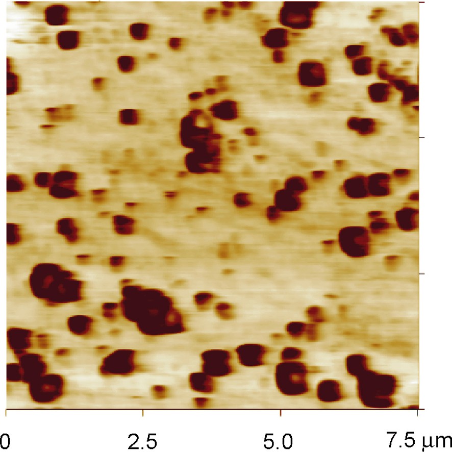
Contact mode AFM image of nanopore array on n-Si (100) after processing in dilute ammonium fluoride solution at pH > 4.5.
2 Experimental
Details of experimental procedures have been published already in [6,7]. Synchrotron radiation photoelectron spectroscopy (SRPES) experiments were performed at Bessy II at the U 49/2 beamline of the collaborating research group (CRG) between the Brandenburgisch Technische Universitaet Cottbus, the Technical Universitaet Darmstadt and the Hahn-Meitner-Institut (HMI) Berlin. AFM experiments were done at the HMI using a nanoscope III microscope in contact mode. The preparation of solutions, electrochemical processing and transfer between electrochemical environment into ultra high vacuum (UHV) has been described earlier in [8].
3 Results and discussion
Fig. 2 shows SRPES data for three rather distinct surface conditions: (i) the electrochemical H termination, (ii) after photooxidation with a charge passed corresponding to the dissolution of one bilayer of Si and (iii) at the first photocurrent maximum of the meanwhile well-known I–V characteristic. The photon energy has been tuned to reach highest possible surface sensitivity for each core level. The inelastic mean free scattering length is = x, y and for Si 2p, O 1s and F 1s, respectively.

SRPES analysis of n-Si (111) for three surface conditions; (a) electrochemical (1 × 1) H-terminated; (b) after potential scan from open circuit (ocp) to + 0.15 V vs. ocp; (c) sample emersion at the first photocurrent maximum of the I–V characteristic; solution 0.1 M NH4F, pH 4; Si 2p, O 1s and F 1s levels are shown.
The envelope shape of the spin-orbit resolved Si 2p1/2 and Si 2p3/2 levels shows a distinct deviation from the expected 2:1 peak intensity ratio (3/2:1/2). Compared to the curve for the H-terminated surface, shoulders and new structure evolve at the higher energy side of the Si 2p1/2 peak. The O 1s line shifts to higher binding energy (EB) after processing at the current maximum and a corresponding low-energy shoulder becomes visible in the F 1s spectrum.
Deconvolution of the 2p levels yields structure that is shifted by 0.23, 0.8, 1.0, 2.3 and ~ 3.5 eV. From comparison of Si partial charge calculations of postulated reaction intermediates in the divalent dissolution process using density functional theory (DFT), most proposed species could be attributed to a shifted signal and hence identified. For the signal shifted by 3.5 eV, surface atoms undergoing a localized corrosion process due to focusing of excess minority carrier trajectories to specific surface sites is assumed [9].
The model proposed assumes that a fully coordinated Si atom has to acquire two positive charges (holes) for dissolution via solvolytic splitting of backbonds. The deflection of minority carriers to these sites results from immobilization of anions at reentrant sites and along step edges of the atomic surface terraces producing high local electrostatic fields. Since the consecutive reactions for dissolving such a surface atom involve a sequence of steps, the Si (II) species is assumed to have a large enough lifetime to be detected in the in-system combined electrochemistry/UHV experiment. The reaction with water molecules and HF results in the formation of HSi(OH)2F with H-termination of the underlying Si atoms which are strained to accommodate the H atoms.
The increasing roughness upon processing at and towards the photocurrent maximum (see also Fig. 4) also results obviously in more water bound by capillary forces as indicated by the shift towards higher EB in the O 1s line. Since the current is anodic, F– counterions will be drawn towards the surface to re-establish electroneutrality. Hence the observation of more water is consistent with the occurrence of solvated fluoride anions as seen in the F 1s line.

Deflection AFM image of a mesa-type surface structure (a) and schematic of the imaging process explaining the projection images of inclined crystal facets (b).
Upon electrochemical processing with charge passed in the range of that at the first current maximum, a rather similar surface appearance is revealed by AFM experiments: one finds an intergranular structure consisting of highly corroded areas and mesa-type features, about 100–250 nm large, with atomically flat (111) top surfaces having particular shapes with angular symmetry similarities. Fig. 3 shows various routes from which such features can be obtained: potentiostatic as well as mixed potentiostatic and chronoamperometric experiments using different scan velocities, molarities and pH yield the aforementioned basic surface nanotopography as seen in the example given in Fig. 4. Analyses of the observed angular features and their assignment to specific crystallographic planes and directions allow the reproduction of virtually all observed mesa geometries. It is found that {111}, {110} and {113} oriented facets forming the side walls of the mesas suffice to construct the observed shapes [10]. From the literature, it is known that these surfaces in particular can all be hydrogen terminated in a (1 × 1) manner [11–13] which explains the stability of the mesas, although transitory due to continuing dissolution along their edges.
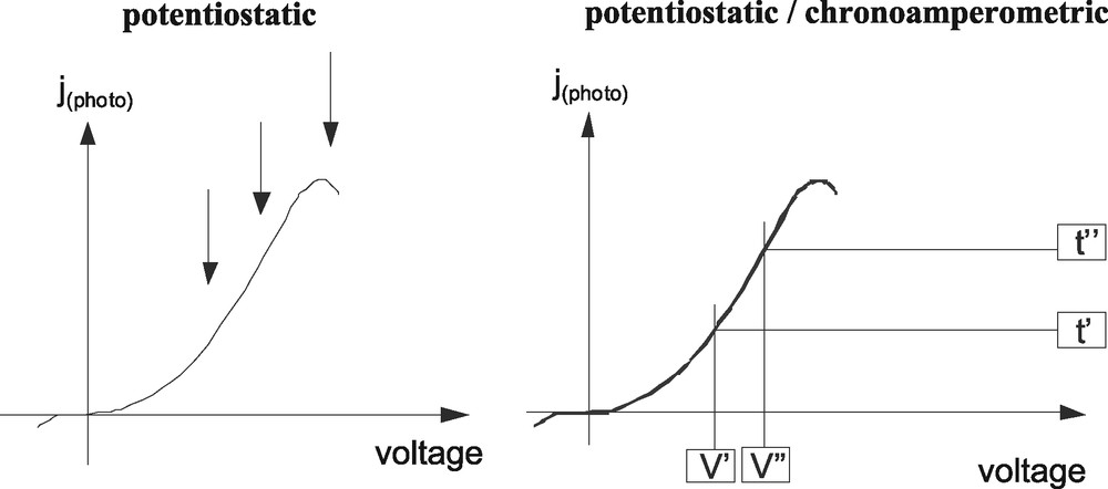
Electrochemical paths for preparation of a granular nanodimensioned surface topography (see text).
Although self-organized structures as described here, if developed properly, could be used for large scale applications, the immediate use of induced structural features, such as indentations [14,15] appears more practical at present. Fig. 5a shows an AFM indent array on oxidized p-type Si (100) made using a specific lithography program. The cross sectional view provides for lateral and depth dimensions.Fig. 5b shows deposited Ag clusters on the former indent seeds. They were obtained by photo-induced electroreduction of Ag ions at regions where the indents thinned or removed the much softer silicon oxide. The locality of the photodeposition results from the passivity of the surface where it is covered by the oxide.
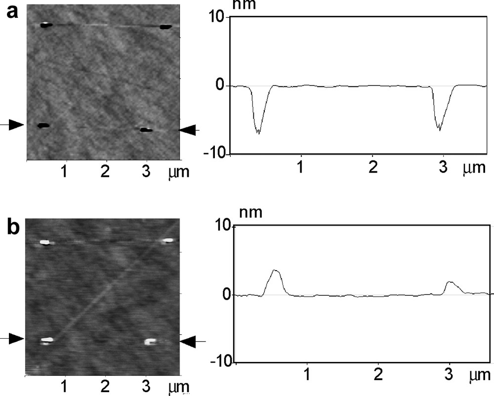
Induced structuring using AFM indents as seeds for metal deposition; (a) indent array on oxidized p-Si (100); (b) local Ag electrodeposits on indented sites.
The localized nanocluster formation represents a precursor experiment in the fabrication of an envisaged nanoemitter Schottky-type solid-state solar cell whose construction scheme is shown in Fig. 6. The geometrical constraints in the metal nanodot arrangement (mutual distance d) are given by considering overlapping circles with radius of the minority carrier diffusion length of Si, i.e. d ≤ Le,h. The dots can be replaced by wires or trenches prepared by chemical or electrochemical processing of seeds (scratches, indents) and penetrating into the semiconductor. In this case, ‘compartment’ cells, where the metal/semiconductor contact reaches deep into the material will exhibit high carrier collection efficiency closer to the rear surface with improved red response. The nanoemitter front contacts are small in size and do practically not contribute to light shading. The insulating oxide between the emitters, needed for local metal deposition, is incorporated into the solar cell structure. The nanoemitters connected to the conductive front TCO contact.
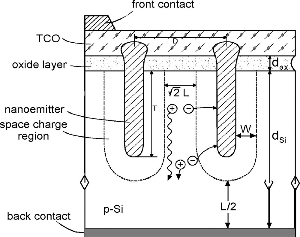
Schematic drawing of a Schottky-junction-type nanoemitter solar cell (see text).
Acknowledgments
The authors like to thank the Interface Engineering team of the HMI and the members of the CRG at Bessy II (R. Hunger, C. Pettenkofer).