

1 Introduction
The conventional methods to study the photoconductive properties of photovoltaic materials can be divided into the following categories [1]: (1) measurement of the current/voltage characteristics under steady-state illumination, (2) laser excitation with time-resolved detection of transient changes in conductivity, (3) time-of-flight (TOF) studies of the charge carrier drift in an electric field and (4) laser excitation with time-resolved detection of transient changes in optical absorption of the conducting species involved. Methods 1–3 require the preparation of thin, i.e. several tens of microns at most, pin-hole free layers of the materials under investigation, to which electrode contacts must be applied. Although these restrictions clearly apply to the fabrication of working photovoltaic devices, complicating factors such as exciton deactivation at the electrode layers, short-circuits, space-charge limited currents and non-ohmic contacts might hinder the ready characterization and comparison of the separate photovoltaic materials involved. Method 4, transient absorption spectroscopy (TAS), is a valuable tool for monitoring the formation and decay of charge carriers in conducting materials. However, since the determination of the extinction coefficients of all the transient species involved is not straightforward, it may be difficult to obtain quantitative data from TAS measurements.
Here we present a powerful complementary method to characterize the photoconductive properties of thin films of photovoltaic materials, the electrodeless flash-photolysis time-resolved microwave conductivity technique (FP-TRMC). By using this technique, which utilizes microwaves to probe the formation and decay of mobile charge carriers, some of the problems associated with the use of electrode contacts might be overcome. Furthermore, since the absolute conductance of the materials involved can be readily determined from its dielectric properties and the microwave cavity characteristics, quantitative data such as charge separation efficiencies and mobilities are easily extracted from microwave measurements.
Due to the low electric field strength (Emax ≈ 100 V/cm) and ultrahigh frequencies (~10 GHz) used, the mobilities obtained are virtually free of domain and grain boundary effects an will mainly reflect the mobility of charge carriers within organized domains of the sample. Moreover, the use of nanosecond time-resolution will ensure that the majority of the mobile charge carriers will be probed before their diffusion to intrinsic trapping sites. The mobility values found can therefore be considered as the maximum mobility that can be attained in a DC experiment with well-organized domains between the electrodes [2].
Microwave conductivity was introduced in the mid-40s by Margenau [3], and extended by Biondi and Brown [4] Brown and Rose [5] to time-resolved studies of the diffusion and recombination of electrons and cations in helium. In the early 1970s Warman et al. [6] and De Haas et al. [7] introduced the pulse-radiolysis time-resolved microwave conductivity (PR-TRMC) to study mobile charge carriers generated by an electron accelerator. The flash-photolysis TRMC technique, which applies nanosecond laser pulses as the radiation source, was developed in the 1980s [8,9] to study the intramolecular charge separation in donor-acceptor compounds and the dynamics of charge carriers in dilute polymers solutions. Recently, a new FP-TRMC facility was built at our laboratory to study charge separation in thin films of photoactive materials [10–24].
Here we present a brief overview of the results obtained with FP-TRMC on photo-induced charge separation in bilayers of a dye-sensitized flat, smooth film of a wide bandgap semiconductor (see Fig. 1) and of dye-sensitized mesoporous nanocrystalline TiO2 films. Details on the sample preparation, the thin film FP-TRMC setup and the data analysis will be provided. Furthermore, theoretical models for the derivation of, among others, the exciton diffusion length and the interfacial electron injection efficiency are presented and discussed.
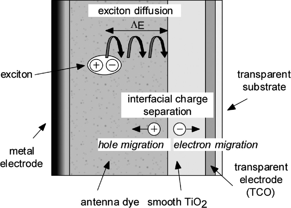
A schematic representation of the fundamental processes of exciton diffusion and interfacial charge separation occurring within a photovoltaic cell which can be studied using the FP-TRMC technique without the necessity of applying electrode layers. The exclusion of such complications is particularly important when attempting to obtain fundamental information on the processes of exciton diffusion within the antenna layer and charge separation at the semiconductor/antenna interface.
2 Experimental methods
2.1 Sample preparation
The substrates used are 1 mm thick 12 × 24 mm2 quartz slides coated with either a smooth (‘SM’) layer of crystalline anatase, prepared by electron beam evaporation [25], or a mesoporous nanocrystalline (‘MN’) layer of anatase TiO2, prepared by doctor blading a colloidal paste followed by high-temperature (450 °C) sintering. The thickness of the TiO2 layers were characteristically 50–100 nm (smooth) and a few microns (mesoporous). Cross-sectional TEM and surface SEM images of typical smooth and mesoporous layers are shown in Fig. 2. The smooth layers were dye-coated by spin-casting solutions of the organic chromophoric compound onto the substrate. Mesoporous layers were dye-coated by immersion of the substrate in a solution of the chromophore for several hours.
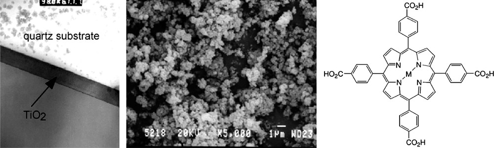
Left: transmission electron microscopy (TEM) cross-sectional image of a smooth, ca. 80-nm-thick, film of anatase TiO2 prepared by electron beam evaporation (EBE). Middle: a scanning electron microscopy (SEM) image of the surface of a film of mesoporous nanocrystalline TiO2. Right: the chemical structure of the porphyrin derivatives investigated, with M = H2, Zn and Pd.
This paper focuses on the results obtained with a series of porphyrin derivatives, i.e. the free-base, zinc, and palladium derivatives of tetracarboxy phenyl-porphyrin; H2TPPC, ZnTPPC and PdTPPC, respectively.
2.2 Optical properties
The optical properties were measured using a 220–2200 nm spectral-range Perkin Elmer λ-900 spectrophotometer fitted with an integrating sphere which allowed the fraction of reflected, FR, and transmitted, FT, light to be measured. The absorption spectra, OD(λ), and attenuation spectra, FA(λ), were determined from OD = – log10[FT/(1 – FR)] and FA = [1 – (FT + FR)]. The latter parameter, which is the fraction of incident photons actually absorbed by the sample, is the more relevant for comparison with the photoconductivity observed in the FP-TRMC measurements.
2.3 Flash-photolysis (FP)
The coated quartz substrate was placed in an X-band (8.2–12.4 GHz) microwave cavity at the position of the maximum electric field strength at resonance, as shown in Fig. 3. After evacuation of the cell to 2 × 10⁻⁵ mbar, it was filled to atmospheric pressure with a 10:1 CO2/SF6 mixture to suppress any possible signals from highly mobile gas phase electrons produced by photo-electron emission from the film [26]. The sample can be positioned such that either illumination via the substrate or via the film side is possible. The end-wall of the cavity consisted of a metal grating covered with a quartz window, which allowed the transmission of the laser beam which was rectangular-shaped to close-to-uniformly illuminate the 1.2 × 2.4 cm2 cross-sectional area of the sample. The laser wavelength could be continuously computer-controlled within the spectral ranges of 240–320 and 420–700 nm. The incident intensity, I0 photons/cm2 per pulse, was in situ monitored by reflecting a small, known percentage of the beam from a quartz plate to a pyroelectric sensor. I0 could be varied over the ranges 1010–1015 photons/cm2 per pulse in the UV and 1011–1015 photons/cm2 per pulse in the visible, using a computer-controlled series of metal-coated, neutral-density filters in tandem. The pulse length was ca. 3 ns in the visible and ca. 2 ns in the UV.
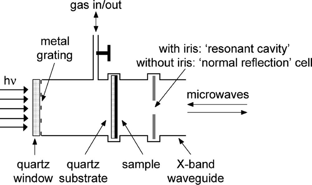
A schematic representation of the microwave cell containing the coated substrate. The sample can be positioned such that illumination either via the substrate or via the film side occurs.
2.4 Time-resolved microwave conductivity detection (TRMC)
The full FP-TRMC setup is schematically depicted in Fig. 4. Changes occurring in the conductance, ΔG, of the sample on flash-photolysis were monitored as changes in the microwave power reflected by the cavity. The transients could be digitally recorded on a variable-range, linear time-base or, in more recent experiments, on a logarithmic time-base covering the range from nanoseconds to milliseconds using a single laser pulse. Signal averaging could be automatically carried out in order to optimize the signal-to-noise ratio. The overall time-response was ca. 18 ns when an iris resonant cavity was used, as in the experiments reported here. In the absence of the iris, a time–response of 1 ns could be achieved. Typical photoconductivity transients are shown in Fig. 5 for uncoated and dye-coated SM samples.

Schematic representation of the thin film FPTRMC setup, including the option of CW background illumination.
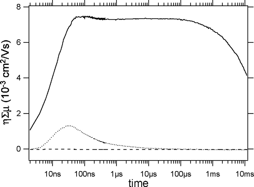
Photoconductivity transients recorded on a logarithmic time-base for 3-ns flash-photolysis at 430 nm of H2TPPC-coated SM TiO2 layer (full trace), an uncoated SM TiO2 layer (dotted trace) and a quartz substrate coated only with the porphyrin (dashed trace). From Ref. [18].
2.5 FP-TRMC data analysis
The absolute value of the conductance change could be determined from the known cavity characteristics and the dielectric properties of the sample. The product of the quantum yield for charge separation per incident photon, η, and the sum of the charge carrier mobilities, Σμ, was calculated from the maximum value of the conductance, ΔGmax, according to
| (1) |
In Eq. (1), e is the elementary charge and β = 2.3 is the ratio of the broad to narrow internal dimensions of the waveguide. For comparison with working device measurements, η is sometimes referred to as ‘IPCSE’, the incident-photon-to-charge separation efficiency. Since IPCSE values are derived in the absence of electrode layers, they can be considered as an upper limit to the IPCE, the incident-photon-to-current-collection efficiency that can be expected for a complete working device.
The product of the quantum yield per absorbed photon, ϕ, and Σμ is related to the IPCSE value simply by
| (2) |
In the experiments described here the conductivity transients result from the formation of highly mobile conduction band electrons in the semiconductor component of the layer. Σμ is therefore equal to the electron mobility in TiO2 alone, μe(TiO2). The value of μe(TiO2) can be determined by direct bandgap excitation of the TiO2 using 300-nm light for which the quantum yield of electrons is assumed to be unity. This value of μe(TiO2) can then be used to make absolute estimates of the yield parameters, η and ϕ, for the indirect formation of electrons via charge injection from the dye layer on photoexcitation in the visible [14,20].
3 Brief summary of results
3.1 Bare TiO2; direct bandgap excitation
As mentioned in the previous section, the conductive properties of bare TiO2 layers can be characterized by direct bandgap excitation in the UV. In fact, even for dye-coated layers, 300 nm photons are invariably preferentially absorbed by the semiconductor because of its extremely high extinction coefficient at that wavelength so that estimates of μe(TiO2) can be made in situ even for the dye-coated layers.
The magnitude of the photoconductivity and the dependence on light intensity are dramatically different for smooth or mesoporous layers, as illustrated by the results in Fig. 6. The former yields values of ϕ Σμ (= μe(TiO2)) which are more than an order of magnitude larger than for the latter, with values of the electron mobility of approximately 2 cm2/Vs; very close to values determined for macrocrystalline anatase by other methods [27]. Furthermore, while the smooth layers show little dependence on intensity up to 1013 photons/cm2 per pulse, the mesoporous layers invariably display an initial increase in photoconductivity with increasing intensity, as shown in Fig. 6.
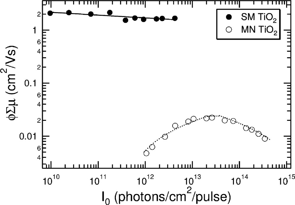
The intensity dependence of the product of the quantum yield (per absorbed photon), ϕ Σμ, on 300 nm photoexcitation of uncoated layers of SM TiO2 (filled squares) and 9-nm particle size MN TiO2 (open circles).
This initial superlinear increase in photoconductivity for MN TiO2 is explained in terms of equilibrium (surface) trapping within the nanocrystalline particulate matrix with the trapping sites becoming increasingly filled as the intensity increases. That this is the underlying reason has been shown by carrying out FP-TRMC measurements on a sample, which was exposed to continuous-wave (CW) background UV illumination. Under these pre-saturation conditions much larger photoconductivity transients were observed at low intensities, while the effect of an increase with increasing intensity was absent, as shown by the data in Fig. 7. A trap-free electron mobility in these 9-nm MN TiO2 particles of 0.034 cm2/Vs was derived. The phenomenon of electron trapping and the influence of adsorbed sensitizer has been discussed more fully in a recent publication [20].

The intensity dependence of ϕ Σμ for a bare MN TiO2 film on pulsed illumination with 300-nm light, in the absence (open squares) and presence (filled diamonds) of 40 μW/cm2 CW UV background illumination. The upper scale is the average number of photoexcitations per nanoparticle. From Ref. [20].
3.2 Visible-wavelength action spectra of porphyrin-coated TiO2
The sensitization effect of a dye layer is illustrated by the transients shown in Fig. 5 for photoexcitation at 430 nm. For a porphyrin layer alone, no measurable photoconductivity is observed. For the uncoated TiO2 a rapidly decaying transient is observed, which is attributed to sub-bandgap excitation of the semiconductor [14,19]. However, with the coating of tetracarboxy phenyl-porphyrin (H2TPPC), a very much larger photoconductivity is found, which only decays on a millisecond timescale. This is attributed to the production of electrons in the semiconductor layer via interfacial charge separation initiated by excitons formed within the porphyrin layer.
Since the excitation wavelength of the laser can be varied continuously from 420 to 700 nm, photoconductivity action spectra can be constructed over the complete visible range. Such a spectral dependence is shown in Fig. 8 for an H2TPPC/SM–TiO2 bilayer. This figure also illustrates one of the advantages of the present technique, the absence of electrode layers, which allows the substrate to be easily reversed within the microwave cell and illumination of either the front (dye-coated) side or the back (quartz/semiconductor substrate) side. As a result of the different (exponentially decaying) absorption profiles within the dye, this leads to entirely different dependences of the IPCSE on the thickness of the coating. As can be seen, there is good agreement between the IPCSE spectrum for illumination through the semiconductor side and the measured attenuation spectrum of the sample, as expected on the basis of the antenna function proposed. Furthermore, the dramatically reduced charge separation efficiency in the Soret band region (400–450 nm) on illumination through the dye clearly demonstrates the effect of optical filtering by the sensitizer.
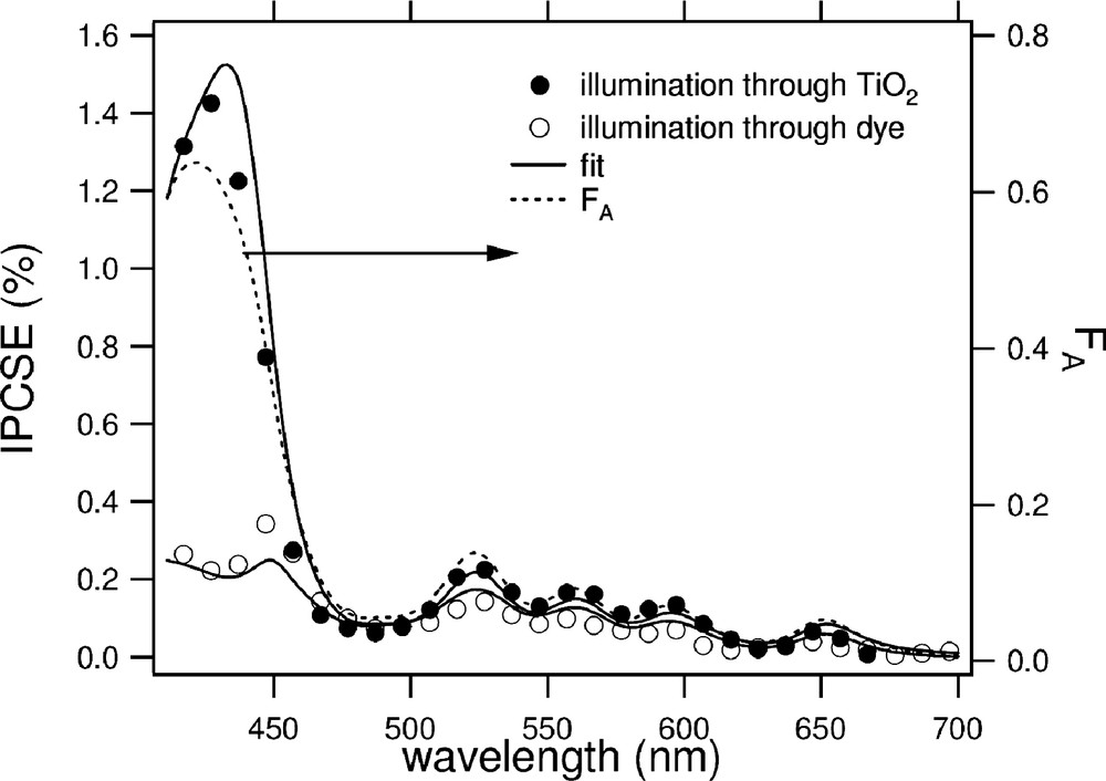
Wavelength dependence of the IPCSE for a 60-nm-thick H2TPPC layer spin-coated onto a smooth, 80-nm-thick layer of anatase TiO2 on illumination via the TiO2 side (filled circles) or the dye side (open circles). The dotted line represents the measured photon attenuation spectrum of the bilayer. The solid lines are fits to analytical solutions to the diffusion equation, yielding an H2TPPC exciton diffusion length of 0.8 nm; see text for details.
Information can be obtained on the exciton diffusion length by studying the effect of varying the thickness of the dye coating in a bilayer. By solving the diffusion equations for exciton migration and charge injection at the dye/semiconductor interface, it is possible to calculate the expected thickness dependence and, upon comparison with experimental TRMC data, derive values of the exciton diffusion length, ΛE, and the efficiency of interfacial electron injection, ϕinj. Furthermore, if the wavelength dependence of the absorption coefficient, α, of the sensitizer is known, it is possible to fit the measured action spectra obtained on front- and back-side illumination to the analytical solutions of the diffusion equation. An example of this is shown in Fig. 8, which demonstrates the marked influence of optical filtering by the antenna layer. A full description of the measurements and the analytical solutions to the diffusion equations for front- or back-side illumination and for reflection or absorption of excitons at the dye/gas interface is given in a recent publication [19].
We note here that the application of steady-state diffusion equations is in fact only valid if the exciton lifetime is much shorter than the length of the illuminating pulse used. For H2TPPC, this condition is fulfilled since its exciton lifetime is much shorter than the laser pulse length of 3 ns. In the following section we describe results on triplet sensitization for which this condition does not apply and non steady-state, numerical computational methods have to be used to describe the data.
3.3 Delayed charge injection from triplet states [15,24]
In Fig. 9 are shown the photoconductivity transients observed on photoexcitation at 430 nm of metal-free, zinc, and palladium derivatives of tetracarboxy phenyl-porphyrin spin-coated onto a smooth, ca. 80-nm-thick layer of TiO2.
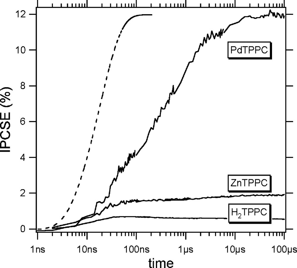
Photoconductivity transients on flash-photolysis (3 ns, 430 nm, ca. 3 × 10¹² photons/cm2) of bilayers of TiO2 coated with the (metallo) porphyrin derivatives indicated. The photoconductivity is expressed as the incident-photon-to-charge separation efficiency, IPCSE. Also shown, as the dashed line, is the integrated intensity during the pulse convoluted with the 18 ns response time of detection. Note the logarithmic timescale. From Ref. [15].
The results illustrate the dramatic differences in magnitude of the transients despite the similarity of the antenna layer thicknesses (ca. 40 nm) and optical densities at the Soret band maximum. In addition to the large differences, particularly surprising is the large after-pulse growth of the conductivity for the palladium derivative over microseconds and the ultimate large value of ca. 12% reached for the IPCSE; much larger than found for any other dye-coated TiO2 bilayer.
The delayed growth has been attributed to sensitization of the TiO2 via the triplet state of PdTPPC, which, because of its long lifetime, can diffuse to the interface from within the antenna layer and inject an electron into the semiconductor many microseconds after the end of the laser pulse. The large difference between the TPPC derivatives has been attributed to the heavy-metal effect of the central Pd atom which lowers the forbiddenness of intersystem crossing and allows the nominal triplet state to diffuse via a Förster-type mechanism rather than the much less efficient Dexter mechanism which is usually assumed to apply for (pure) triplet states. As pointed out in the previous section, steady-state approaches to the exciton diffusion problem cannot be applied to cases for which the exciton lifetime is comparable or longer than the period of illumination, which is clearly the case for PdTPPC. Accordingly we have carried out numerical Monte Carlo type calculations of the exciton diffusion and interfacial charge separation problem [24]. The results of such calculations are shown in Fig. 10, where best fits are shown to PdTPPC transients for different incident light intensities. From the fitting procedure the following parameters could be determined; a) the exciton diffusion coefficient, 8 × 10⁻¹¹ m2/s, b) the reaction radius for exciton-exciton annihilation, 1.5 nm, and the efficiency of interfacial charge separation, 0.44. Taking the triplet state lifetime to be at least 10 μs results in an estimated exciton diffusion length in PdTPPC in excess of 28 nm.
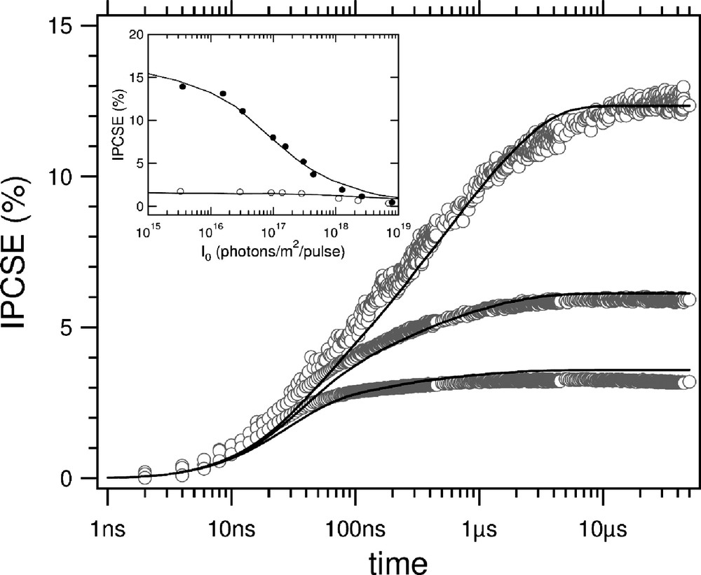
Monte Carlo calculated fits (full lines) to the after-pulse growth of the conductivity on (3 ns, 430 nm) flash-photolysis of a PdTPPC-coated smooth layer of TiO2, for incident intensities (from top to bottom) of 2.5 × 10¹⁶, 23 × 1016 and 86 × 1016 photons/m2 per pulse. The inset shows the full experimental and simulated intensity dependence at 20 ns and 10 μs. The parameters derived from the fits are given in the text. From Ref. [24].
3.4 Porphyrin-coated mesoporous TiO2 [20]
In Fig. 11 are shown the photoconductivity transients observed on laser flash-photolysis at 520 nm of a 3-μm-thick film of Solaronix Ti-Nanoxide HT coated with H2TPPC together with results for the semiconductor and porphyrin alone. As for the SM film shown in Fig. 5, the presence of the porphyrin coating results in very much larger signals, indicating sensitization by the antenna layer to occur. The similarity between the decay kinetics for the uncoated and the dye-sensitized MN TiO2 film, which are also independent of direct (UV light) or sensitized (visible light) charge separation, implies that electron trapping is the major decay pathway on this timescale for mobile electrons in MN TiO2. The maximum IPCSE value resulting from photoexcitations produced in the porphyrin layer on excitation in the Soret band was 18%, which is much larger than the value of only 1% found for the SM layer. The considerably greater efficiency of using a nanocrystalline mesoporous layer rather than a simple bilayer structure is therefore apparent.
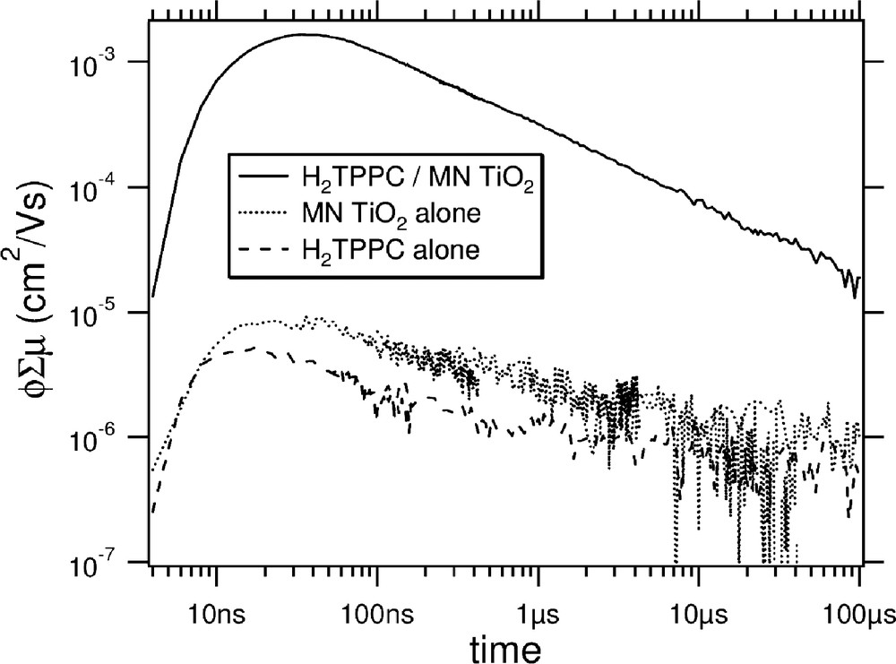
Absorbed-photon-normalized conductivity transients observed on photoexcitation at 520 nm of an H2TPPC film alone (dashed trace), a mesoporous (Solaronix) TiO2 film uncoated (dotted trace), and coated with H2TPPC (solid trace). The values of I0 were 4.4 × 10¹⁵, 6.8 × 10¹⁵ and 3.2 × 10¹⁴ photons/cm2 per pulse, respectively. From Ref. [20].
4 Conclusions
We have presented a brief overview of the application of the FP-TRMC technique. Using this electrodeless technique, valuable parameters of photoactive thin films such as the transient behavior, photoconductivity action spectrum and intensity dependence of direct and sensitized charge separation can be measured. Furthermore, we have demonstrated that with the aid of analytical and Monte Carlo models, the derivation of exciton diffusion lengths and interfacial charge injection efficiencies is possible.
Acknowledgements
Martien Vermeulen, John Suykerbuyk and Paul Rijkers are gratefully acknowledged for their technical assistance. This research was supported financially by the Netherlands Organization for Scientific Research (NWO).