

1 Introduction
The extremely thin absorber (eta)-solar cell is a photovoltaic device using a thin absorber layer sandwiched between two interpenetrating transparent (wide band gap) semiconductors (Eg > 3 eV) [1,2]. It consists of a nano- or micro-structured layer which also serves as an n-type window layer to the cell, an absorber (1.1 < Eg < 1.8 eV) conformally deposited on this layer, and a void filling p-type material with a metallic back contact. The physical bases of the eta-solar cell are the light absorption and the pin diode principle, as can be seen in Fig. 1.
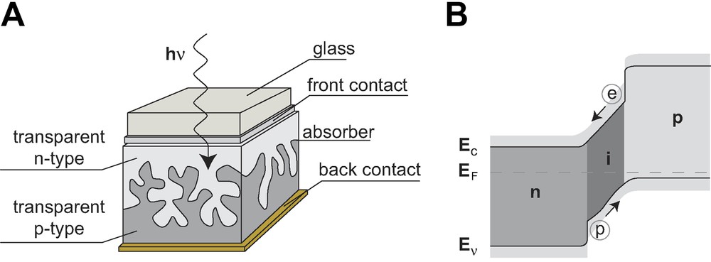
(a) Schema of the eta-solar cell and (b) band diagram.
As can be inferred from its band diagram (Fig. 1b), at the n-type/absorber interface the junction field and the band alignment are such that electron transfer can occur only from the absorber to the n-contact, while hole transfer is blocked due to the large valence band offset. Hole transport can occur only from the absorber to the p-type layer. Therefore, the device enforces the separation of excess charge, driven by the internal electric field and the band alignment.
One of the keys of this type of device is an extreme surface enlargement, by a factor between 10 and 100 relative to flat films that allows a reduction in the absorber thickness of the same order of magnitude. This reduction in the absorber thickness significantly improves the collection probability, due to the shorter transport path length for the excited carriers. Electron-hole pairs photogenerated in the absorber do not need to travel over large distances before being separated and collected because the absorber is very thin (a few tens of nanometers) and is located in the electric field formed at the p–n junction of two wide band gap semiconductors (Fig. 1a). At the same time, scattering at the internal interfaces of the structure will increase the optical path through the sample and thereby enhance the photon absorption [3]. This phenomenon is known as the light-trapping effect.
In order to get a good light-trapping of solar light, the layer used as window should have a structure with a typical length scale in the wavelength range of solar light. In order to obtain a reduction of the electronic path, a deep structuring in the 50–300 nm length scale is desirable. With these conditions, the optical and the electronic properties of the heterostructure are advantageous for photovoltaic applications.
Until now, the most frequently used materials as window and n-type material for the eta-solar cell have been porous TiO2 [4,5] and ZnO nanowire films [6–8]. As inorganic absorber materials, CdTe [1,6], HgCdTe [9] CuInS2 [10], a-Si:H [7] and Se [11] have been used. Finally, as a void filling and p-type material, CuSCN [5,10,11] and ZnTe [12] have been used.
A review of the literature shows that there has been an increasing effort to obtain uniform deposition of the absorber on the nano-structured or porous n-type materials by different techniques. For example, CdTe by electrochemical deposition [5], vapor-phase epitaxy (VPE) [6] and metal organic chemical vapor deposition (MOCVD) [8], a-Si:H by plasma-assisted chemical vapor deposition (CVD) [7] and CuInS2 by ion layer gas reaction (ILGAR) [10]. Nevertheless, to our knowledge, there are few published results of complete eta-solar cells. Tennakone et al. [11] reported the TiO2/Se/CuSCN heterostructure as a photovoltaic cell with an energy conversion efficiency ~ 0.13% in 1998. Three years later, the Könemkamp group proposed the TiO2/CuInS2/CuSCN heterostructure as a good candidate to act as an eta-solar cell [10]. They studied the dependence of the photocurrent as a function of the absorber layer thickness and they showed the rectifying behavior of their samples under dark conditions, but did not report its energy conversion efficiency.
The work in this paper reports on eta-solar cells based on ZnO nanowire films electrodeposited on transparent conducting substrates as n-type material. As absorber material, CdSe, a II–VI semiconductor was deposited electrochemically. In order to complete the eta-solar cell, as p-type material, we deposited CuSCN by chemical solution deposition [12]. The morphology, structural and optical properties of the layers were analyzed as they were built up. As a final characterization, we measured illuminated and dark iV curves of a series of complete eta-solar cells.
2 Experimental
ZnO/CdSe/CuSCN eta-solar cells were made by using easily accessible electrochemical and solution deposition techniques on commercial conducting glass/SnO2:F substrates (10 Ω/□) from SOLEMS SA. The details of the deposition process of each material will be explained in Section 4.
The morphology and crystalline structure of the different layers were analyzed using a Leica Stereoscan 440 scanning electron microscope (SEM) and an automated PW 1710 Phillips X-ray powder diffractometer. The optical properties (transmittance and reflectance) were measured at room temperature in the 300–1200-nm wavelength range with a Hitachi UV–VIS–NIR4001 spectrophotometer fitted with an integrating sphere. Photoconversion was measured by i–V curves in the dark and under illumination, contacting to the SnO2:F substrate and an evaporated gold contact. Samples were illuminated using a halogen lamp directed through an optical fiber bundle. The optical fiber was used to minimize heating of the sample by the light source. 360 W m–2 was the maximum illumination possible with this source. The power output of the light source was measured before and after the cell measurement using an Eplab Spectral Pyranometer from Eppley Laboratory. Finally, the spectral photoresponse of the cells was measured in the wavelength range of 400–1100 nm. The illumination consisted of a 75-W tungsten–iodine lamp and a Jobin Yvon H20 monochromator under remote control. The excitation light was chopped for synchronous detection and the light flux was measured using a calibrated photodiode.
3 Choice of materials
The energy gap (Eg ~ 3.35 eV) [13] of ZnO joined with the nanowire morphology of the ZnO electrodeposited films on conventional transparent conducting substrates [7] make this type of film a good candidate to be used as a nano-structured window and n-type material for the eta-solar cells. As the nanowires are not in direct contact with each other, there is no lateral conduction among them, and electronic transport in the direction of the nanowire axis is possible. The inferred values for their carrier concentration and electron mobility were 1020 cm–3 and 23 (cm2 V s–1), respectively [7]. These values favor carrier transport because the carrier length is substantially shortened and carrier transfer is made efficiently due to noticeable mobility.
The compound most frequently used as p-type and a void filling material in inorganic eta-solar cells is CuSCN (Eg ~ 3.4 eV) [5,10,11]. This material has also been used in similar solar cells with dye as absorber, obtaining promising energy efficiencies [14,15]. These results, together with the ease and availability of the technique used to deposit it, suggest the use of CuSCN as p-type material.
The ideal bandgap for the absorber material lies in the range of 1.1–1.8 eV, with a value of 1.5 eV being optimal. For this reason CdTe (Eg ~ 1.5 eV) is a frequent choice for use as an inorganic absorber in the eta-solar cells [1,6]. Nevertheless, poor photocurrent has been obtained in the ZnO/CdTe/CuSCN heterostructure [8].
In this work we used CdSe (1.7 eV) as an alternative absorber material. The band diagram of the ZnO/CdSe/CuSCN heterostructure is shown in Fig. 2, using the reported values for electron affinities of ZnO, CdSe [16] and CuSCN [21]. According to the band diagram and taking into account the valence and conduction band offsets (Table 1), the heterostructure promotes electron transfer from the absorber to ZnO and hole transfer from the absorber to CuSCN. Therefore CdSe is a good candidate to act as absorber in ZnO/absorber/CuSCN eta-solar cells because its conduction and valence bands are in a favorable position with respect to the n and p-type materials. Furthermore, the CdSe bandgap is in the desired range to achieve high light absorption.
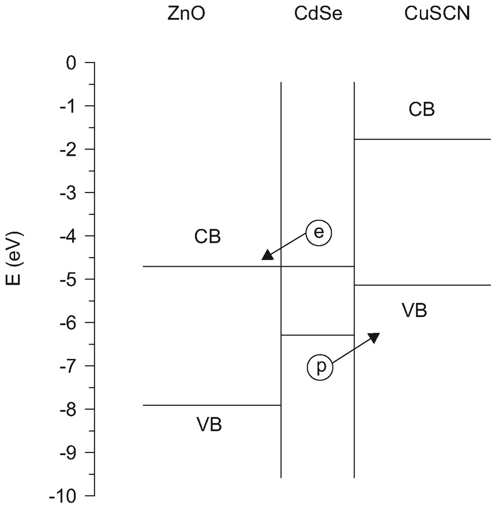
Band diagram of ZnO/CdSe/CuSCN heterostructure. CB and VB are the conduction and valence bands, respectively.
Valence and conduction band offsets at different interfaces of the heterostructure
| ZnO/CdSe/CuSCN | ||
| VB offset (eV) | CB offset (eV) | |
| ZnO/absorber | 1.6 | ~0 |
| Absorber/CuSCN | 1.1 | 2.9 |
4 Results
4.1 n-Type material: ZnO
4.1.1 Deposition process
A thin continuous ZnO layer (ZnOsp) was deposited by spray pyrolysis before ZnO electrodeposition (ZnOed). This layer was deposited in order to avoid any contact and, consequent short-circuiting between the SnO2:F and CuSCN layers. It was deposited from a 0.1 M zinc acetate dihydrate (Zn(C2H3O2)·2 H2O) and 0.2 M acetic acid (C2H4O6) solution. The solvent was a 25:75 (by volume) water/ethanol mixture [17]. The layer was deposited by spraying ~1 ml of solution onto a conducting glass substrate (4 × 1 cm2) pre-heated to ~450 °C. The spraying process consisted of 15 cycles (2 s with spray and 10 s without spray). These cycles avoid an abrupt decrease of the substrate temperature and, therefore, non-uniform ZnO deposition due to the condensation of the spray.
ZnO nanowires were electrodeposited from aqueous solution at 80 °C. The Zn and oxygen precursors were ZnCl2 (5 × 10⁻⁴ M) and bubbling oxygen (saturation) dissolved in ultrapure water (18 MΩ cm) with 0.1 M KCl as the supporting electrolyte [18]. Electrodeposition of ZnO films according to reaction 1, was carried out at –1 V versus SCE (Saturated Calomel Electrode) on conducting glass (1 × 2 cm2) covered by a sprayed ZnO layer.
| (1) |
Different densities of charge (0.5–25 C cm–2) were used for the ZnO electrodeposited films in order to obtain the nanowire structure with desired dimensions to act as window of the eta-solar cell.
4.1.2 Morphology
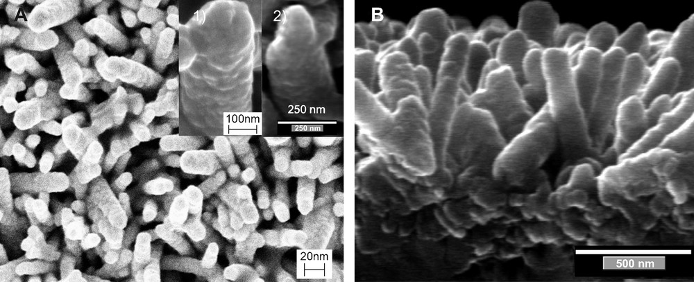
SEM figures of each layer of the glass/SnO2:F/ZnOsp/ZnOed samples and the cross section of these samples are shown in Fig. 3.
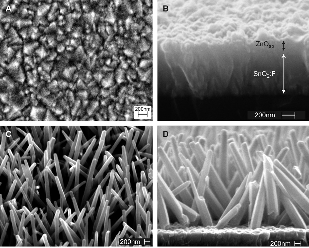
SEM figures: (a) the SnO2:F surface of the conducting glass, (b) ZnO layer deposited by spray pyrolysis on conducting glass, (c) planar view (45° tilted) and (d) cross section of electrodeposited ZnO (20 C cm–2) on a glass/SnO2:F/ZnOsp sample.
The SnO2:F layer of the conducting glass substrates is polycrystalline with grains 100–300 nm diameter, as can be observed in Fig. 3a. The roughness produced by these grains remains in the ZnO layer deposited by spray pyrolysis. The sprayed layer is approximately 150 nm thick (Fig. 3b).
In the case of ZnO electrodeposited on a glass/SnO2:F/ZnOsp substrate, the layer is constituted of free-standing ZnO nanowires, oriented almost perpendicularly to the substrate (Fig. 3c,d). A systematic study (not shown here) revealed that the height of the wires increases as a function of the density of charge used in the electrodeposition process. Meanwhile, their diameter remains approximately constant in the studied range. For a charge density of 20 C cm–2 used to make ZnO, the height of the wires is close to 2 μm and the diameter is within the range of 100–200 nm. Considering the surface area of the wires and evaluating their density, the surface enlargement factor can be estimated. The surface area of an average nanowire (2 μm height and 150 nm in diameter) is ~ 1 × 10⁻⁸ cm2 and the typical density of the nanowires is ~ 1 × 109 cm–2. Then, a surface enlargement factor close to 10 can be estimated for these ZnO nanowire samples.
Therefore, after the analysis of the SEM images, we can conclude that the glass/SnO2:F/ZnOsp/ZnOed samples (using 20 C cm–2 for the ZnO electrodeposition) present a suitable morphology to be used as window for an eta-solar-cell device. The dimensions of the ZnO nanowires are in the range desired to produce a good light-trapping effect after absorber coverage and, joined with their density, produce a noticeable surface enlargement factor. Thus, except in the cases of additional remarks, the density of charge used in the ZnO electrodeposition of all samples analyzed in this work was 20 C cm–2.
4.1.3 Crystalline structure
The XRD patterns of the different layers of the glass/SnO2:F/ZnOsp/ZnOed were recorded. The SnO2:F layer crystallizes as a tetragonal phase [19], as can be observed in Fig. 4a. One small unidentified peak (2θ ~ 31.3°) is found in the XRD pattern. The origin of this peak is not clear. The coincidence between its 2θ value and the 2θ value of the (310) peak from the monoclinic phase of the tin oxide fluorine ((Sn2O2F4)Sn2) [20] could indicate the presence of some inclusions of this compound in the conducting substrates. A small broadening on the left side of the (310) peak of SnO2 is observed in Fig. 3a. This broadening could be caused by the contribution of a small peak with a 2θ value corresponding to the (620) peak of the monoclinic phase of the (Sn2O2F4)Sn2. This peak could confirm the hypothesis of the presence of some (Sn2O2F4)Sn2 inclusions with a preferential orientation along the [310] direction. The presence of small peaks corresponding to the hexagonal phase of ZnO in the XRD pattern of glass/SnO2:F/ZnOsp (Fig. 4b), confirms that a thin layer of ZnO covers the conducting glass substrate after spray pyrolysis. This layer does not present a clear preferential orientation. However, the ZnO peak intensity is too low to draw this conclusion.

XRD patterns: (a) conducting glass (glass/SnO2:F), (b) ZnO layer deposited by spray pyrolysis on conducting glass, (c) ZnO electrodeposited on a glass/SnO2:F/ZnOsp substrate. The indexed peaks in figures (b) and (c) correspond to the hexagonal wurtzite phase of ZnO (lattice parameters: a = 3.253 Å and c = 5.213 Å).
Finally, the XRD pattern of the glass/SnO2:F/ZnOsp/ZnOed sample shows that the ZnO nanowires crystallize with the hexagonal wurtzite structure. The highest intensity corresponds to the (0002) peak, confirming the preferential growth orientation along the [0001] direction, as can be deduced from SEM (Figs. 3b and 3c).
4.1.4 Optical properties
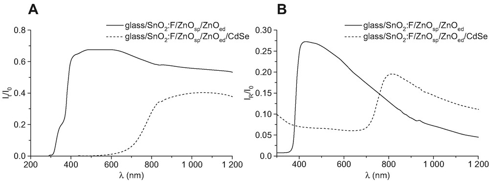
The transmittance and reflectance of the glass/SnO2:F/ZnOsp/ZnOed samples are shown in Fig. 5. The sequence of the measurements was the same as for SEM and XRD measurements (glass/SnO2:F, glass/SnO2:F/ZnOsp and glass/SnO2:F/ZnOsp/ZnOed).
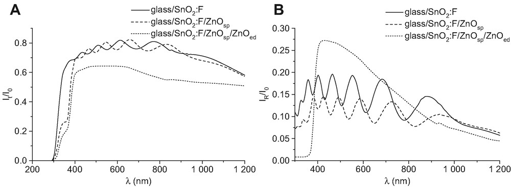
Optical properties of the glass/SnO2:F/ZnOsp/ZnOed sample. (a) Transmittance. (b) Reflectance.
The presence of a thin ZnO layer after the spray deposition process (see Fig. 3b) has been confirmed by the shift in the absorption edge (Fig. 5a), and the small shift in the interference oscillations, with respect to the corresponding naked conducting glass substrate (glass/SnO2:F). The presence of interference oscillations indicates that the approximately flat morphology of the SnO2:F layer is kept in the ZnOsp layer. The wavelength range analyzed is not enough to estimate the thickness of this layer because the most visible interference oscillations present in the optical transmittance are due to the SnO2:F layer. The loss of the flat morphology in the samples after ZnO electrodeposition produces the disappearance of the optical interference oscillations. The light scattering produced by the nanostructure, due to the size of the wires and the distance between them, is clearly observed in Fig. 5b, which shows a noticeable change in reflectance after ZnO electrodeposition. Note that optical reflectance measurements have been made using a spectrophotometer fitted with an integrating sphere. Therefore, the reflections in all directions were measured.
The energy gap (Eg) of different layers was estimated by using the relation for direct optical transition OD = A (hν – Eg)1/2 where OD, A and hν are the optical density, a constant and the incident energy, respectively [21]. An Eg ~ 4.22 eV was estimated for the SnO2:F layer. This value lies in the wide reported range (3.9–4.6 eV) for the bandgap of SnO2 [22]. Rakhshani et al. [23] attributed the scatter in the reported values to the different doping values of the SnO2 samples and concluded that doping with fluorine enhances the film's transparency at short wavelengths. For sprayed and electrodeposited ZnO layers, an Eg ~ 3.31 eV was found. This value is also in good correlation with reported values [24].
4.2 Thin absorber: CdSe
4.2.1 Deposition process
CdSe was deposited electrochemically from an aqueous alkaline selenosulfate solution (0.05 M cadmium acetate (C4H6CdO4), 0.1 M nitrilotriacetic acid trisodium salt (C6H6NO6Na3) and 0.05 M selenosulfate, with excess sulfite) [25–27] at room temperature. The pH was adjusted to ~ 8 by adding acetic acid. A two-electrode electrochemical cell was used with the glass/SnO2:F/ZnOsp/ZnOed sample as the cathode and a Pt wire as the counter electrode. Electrodeposition of CdSe films according to reaction 2 was carried out under galvanostatic conditions with a current density in the range of –1.5 to –3 mA cm–2.
| (2) |
The deposition parameters (current density and density of charge) were chosen after a photoelectrochemical (PEC) study (not discussed here) made on glass/SnO2:F/ZnOsp/ZnOed/CdSe samples. This study showed that the maximum photocurrent was obtained for a CdSe layer deposited at ~–2.7 mA cm–2 and 0.25 C cm–2. Galvanostatic deposition of CdSe at this current density resulted in potentials starting at –1.5 V and rising to –1.7 V during deposition. Some glass/SnO2:F/ZnOsp/ZnOed/CdSe samples were annealed in air at 350 °C for 1 h.
4.2.2 Morphology
SEM images of the CdSe surface and of the cross section of glass/SnO2:F/ZnOsp/ZnOed/CdSe samples are shown in Fig. 6.
SEM figures. (a) Planar view of the CdSe layer deposited on glass/SnO2:F/ZnOsp/ZnOed. Two high-magnification pictures are shown in the inset: (1) before and (2) after annealing. (b) Cross section of the glass/SnO2:F/ZnOsp/ZnOed/CdSe sample. The amount of charge used in the ZnO electrodeposition in this sample was 15 C cm–2.
The nanowire morphology remains after CdSe deposition. A CdSe layer thickness in the range of 30–40 nm was estimated from a statistical evaluation of the nanowire diameters before and after CdSe deposition. This thickness was compared with that obtained for a CdSe layer deposited under the same conditions (current density and density of charge) on a flat conducting glass substrate. The CdSe thickness on the flat surface is approximately 12 times greater than the estimated CdSe thickness on glass/SnO2:F/ZnOsp/ZnOed samples. This approach to determining area coverage is not conclusive because the potentials for the two depositions were not exactly the same because of differences in conductivity of the two substrates; in addition, it is not clear that the efficiency of deposition was the same in the two cases. Nevertheless, joined with the estimate made in Section 4.1.2, this thickness indicates that the order of magnitude of surface enlargement is 10.
The CdSe layer consists of several grains (insets of Fig. 6a). The magnification of the SEM pictures is not sufficient to estimate the grain size and compare it before and after annealing. In CdSe electrodeposition glass/SnO2:F/ZnOsp/ZnOed samples were immersed into the solution. Then, the solution, and, therefore, the cadmium and selenium precursors, was in contact with all parts of the ZnO nanowires, giving a conformal and highly uniform CdSe deposition along the nanowires (Fig. 6b). The alkaline solution does not etch the ZnO nanowires, as would an acidic solution. This work confirms that electrochemical deposition is a suitable and accessible technique to achieve conformal coverage of nano-structured samples, as proposed by other authors [2,28].
4.2.3 Crystalline structure
XRD patterns of glass/SnO2:F/ZnOsp/ZnOed/CdSe samples before (Fig. 7a) and after (Fig. 7b) annealing were recorded in order to analyze the effects of this process on the crystalline properties of the samples.

XRD pattern of the glass/SnO2:F/ZnOsp/ZnOed/CdSe samples (a) before and (b) after annealing process (350 °C during 1 h). The indexed peaks are the CdSe peaks. C and H mean cubic and hexagonal phases, respectively. (Lattice parameters of the hexagonal structure: a = 4.299 Å, c = 7.010 Å, lattice parameter of the cubic phase: a = 6.077 Å).
The polycrystalline character of the CdSe layer, inferred from the SEM images (insets of Fig. 6a), is confirmed in the XRD pattern. The CdSe layer is constituted of a mixture of cubic [29] and hexagonal phases as attested by the presence of the (100 peak) [30]. The large width of the CdSe peaks in as-deposited samples, can be seen in Fig. 7a. The width of the peaks corresponding to the cubic phase decreased noticeably after annealing. Furthermore, the intensity of the peaks increased by a factor of 1.5. However, the (100) CdSe peak did not change. From this we infer that the annealing process does not affect CdSe crystallites with hexagonal structure, but improves the crystallinity of the cubic phase.
The grain size was estimated using Scherrer's formula:
| (3) |
The CdSe crystallite size was calculated by analyzing (111) and (100) planes for cubic and hexagonal phases, respectively. For the as-deposited CdSe layer, a crystallite size of ~ 5 and ~ 10 nm was estimated for the cubic and hexagonal phases, respectively. The size of cubic crystals increases to ~ 15 nm after annealing, whereas the size of hexagonal crystals does not change. The CdSe layer shows a mean grain size of ~ 10–15 nm after annealing. Similar crystallite sizes have been reported in CdSe layers chemically deposited on amorphous glass substrates and annealed at 300 °C in air for 4 h [33].
We can conclude that air annealing produces a recrystallization process involving CdSe cubic crystals, leading to an average grain size of ~ 10–15 nm. For the eta-solar cell application, an increase of the grain size is desirable in order to reduce the deleterious effects of grain boundary trap states. Therefore, the noticeable increase of the mean grain size during the annealing process could improve the efficiency of eta-solar cells with CdSe as absorber.
4.2.4 Optical properties
The optical transmittance and reflectance of the glass/SnO2:F/ZnOsp/ZnOed/CdSe samples are shown in Fig. 8. We made a comparison with the glass/SnO2:F/ZnOsp/ZnOed samples to clarify the role of the CdSe layer in the glass/SnO2:F/ZnOsp/ZnOed/CdSe heterostructure.
Optical properties of the glass/SnO2:F/ZnOsp/ZnOed/CdSe sample. (a) Transmittance. (b) Reflectance.
An optical gap of 1.68 eV was estimated for the CdSe layer by using the relation for direct transition. This value is within the reported range for the Eg of CdSe [34]. The origin of the significant optical absorption at wavelengths higher than the CdSe bandgap in the glass/SnO2:F/ZnOsp/ZnOed/CdSe samples is not clear. This absorption decreases after annealing; thus, it could be related to the grain size of the CdSe layer.
We calculated RE and AE in the 400–800 nm region of the solar spectrum (AM1.5), for the glass/SnO2:F/ZnOsp/ZnOed/CdSe samples, according to the following equations [6].
and
where J0 is the photon flux. The values obtained are ~ 8% and ~ 89% for RE and AE, respectively, showing that efficient light-trapping is achieved. AE obtained with a few tens of nanometers of absorber material thickness is similar to that obtained in crystalline Si with a thickness of ~100 μm [35].
4.3 p-Type material: CuSCN
4.3.1 Deposition process
The CuSCN layer was-deposited from a saturated solution of CuSCN in propylsulfide (15 mg ml–1) [11] on pre-heated ~80 °C glass/SnO2:F/ZnOsp/ZnOed/CdSe samples. The sample was placed on a hotplate to keep it at constant temperature. Following the method of O'Regan et al. [14], the solution was allowed to flow slowly from a pipette while the pipette was moved in a rectangular pattern over the sample, giving an uniform layer. The amount of solution used in the CuSCN deposition process was 0.08–0.12 ml and the covered area was between 1 and 1.5 cm2.
4.3.2 Morphology
SEM photographs of the cross sectional and planar views of glass/SnO2:F/ZnOsp/ZnOed/CdSe/CuSCN samples are shown in Fig. 9. The cross sectional view shows that the sample is compact and dense, indicating that the chemical solution technique favors the penetration of the solution inside the ZnOed/CdSe nanostructure, before propylsulfide evaporation. From Fig. 9 we can conclude that solution volumes on the order of 0.1 ml cm–2 are sufficient to fill the columnar structure and form a layer with thickness of ~2 μm on top of the nanowires. The surface of the CuSCN layer does not show extremely high roughness (inset of Fig. 9). Such approximately flat surface is desired to favor the deposition of a metallic contact on it. Using the techniques described here, ZnO/CdSe/CuSCN samples with a thickness of a few micrometers (2.5–3.5 μm) can be obtained with interfaces which have attractive dimensions to be used as eta-solar cells.
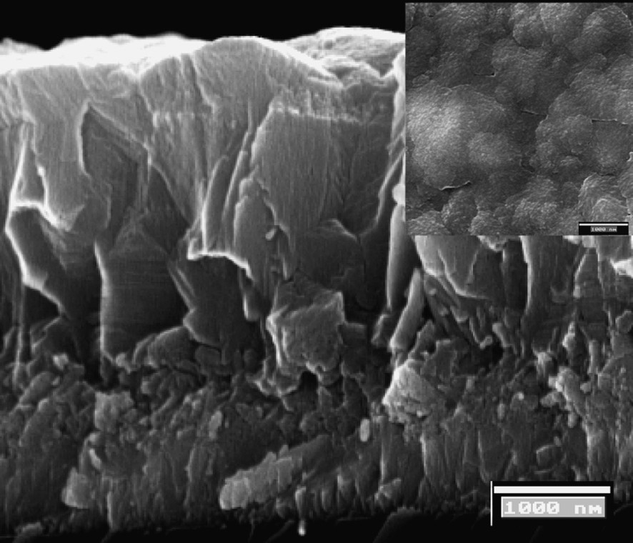
SEM figures: Cross section of a glass/SnO2:F/ZnOsp/ZnOed/CdSe/CuSCN sample. Planar view of the CuSCN layer is shown in the inset. The amount of solution used in the CuSCN deposition was 0.12 ml cm–2. The density of charge used in the ZnO electrodeposition was 15 C cm–2.
4.3.3 Crystalline structure
The XRD pattern of a glass/SnO2:F/ZnOsp/ZnOed/CdSe/CuSCN sample shows that the CuSCN layer crystallizes with the hexagonal β-CuSCN phase (lattice parameters: a = 3.857 Å and c = 16.449 Å) [36] The intensity of the (0003) and (0006) peaks (note the logarithmic scale) indicates a preferential orientation of the CuSCN layer along the [0001] direction (Fig. 10). We have also observed that the CuSCN layer of glass/SnO2:F/ZnOsp/ZnOed/CdSe/CuSCN samples not annealed before CuSCN deposition is more highly oriented than it is in annealed samples. The increase of the CdSe cubic crystallite size after annealing (Fig. 7), promotes a decrease in the orientation of the CuSCN layers along the [0001]direction. As is expected, the hexagonal CdSe phase (lattice parameters: a = 4.299 Å, c = 7.010 Å) favors CuSCN crystallization along the [0001] direction more efficiently than does cubic CdSe (lattice parameter: a = 6.077 Å). This fact shows the influence of the absorber layer, in spite of its thinness, on the crystallization mechanism of CuSCN layer. Then, we can conclude that the absorber layer CdSe acts as a buffer layer on the CuSCN layer deposition.

XRD pattern of glass/SnO2:F/ZnOsp/ZnOed/CdSe/CuSCN samples. The indexed peaks correspond to the hexagonal phase of β-CuSCN (lattice parameters: a = 3.857 Å and c = 16.449 Å). The sample was annealed in air, at 350 °C during 1 h, before CuSCN deposition.
4.3.4 Optical properties
The optical transmittance and reflectance of the glass/SnO2:F/ZnOsp/ZnOed/CdSe/CuSCN samples are shown in Fig. 11. The optical gap of CuSCN cannot be estimated from the transmittance or reflectance of these samples. From the point of view of the eta-solar cell mechanism, the relevant parameters are the optical transmittance and reflectance for the complete heterostructure. No relevant changes are detected after CuSCN deposition in the most important wavelength range (400–800 nm). Nevertheless, in glass/SnO2:F/ZnOsp/ZnOed/CdSe/CuSCN samples a noticeable absorption is observed at wavelengths higher than the CdSe bandgap. The presence of defects in the ZnO/CdSe and CdSe/CuSCN interfaces, related to the small grain size of the CdSe layer, could be the origin of this absorption increase. In fact, at these wavelengths, the optical absorption decreases in annealed samples.
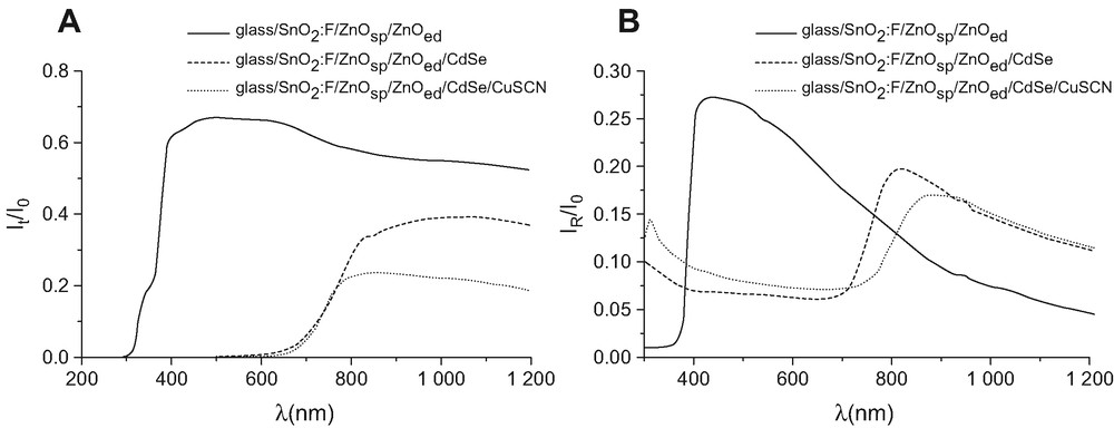
Optical properties of glass/SnO2:F/ZnOsp/ZnOed/CdSe/CuSCN samples. (a) Transmittance. (b) Reflectance.
As a summary of the optical measurements made on different layers of the glass/SnO2:F/ZnOsp/ZnOed/CdSe/CuSCN heterostructure; focusing on eta-solar cell devices, the calculated AE and RE in the 400–800 nm range of the solar spectrum (AM1.5) are reported in Table 2. The RE and AE values show that the p–i–n heterostructure exhibits highly efficient light-trapping, confirming the validity of the choice for application in solar cell devices.
Calculated AE and RE in the 400–800-nm range of the solar spectrum (AM1.5)
| Sample | RE (%) | AE (%) |
| Glass/SnO2:F/ZnOsp/ZnOed | 23 | 12 |
| Glass/SnO2:F/ZnOsp/ZnOed/CdSe | 8 | 89 |
| Glass/SnO2:F/ZnOsp/ZnOed/CdSe/CuSCN | 8 | 89 |
4.4 Electrical characterization of the ZnO/CdSe/CuSCN eta-solar cells
A gold electrical contact was vacuum evaporated on the CuSCN layer to complete the eta-solar cells. These cells were then characterized by i–V curves in the dark and under illumination, and photoconversion efficiency calculated.
Current-voltage measurements were made on the eta-solar cell layers as they were built up. The SnO2:F/ZnO junction is an ohmic contact, and subsequent junctions (ZnO/CdSe, ZnO/CuSCN and CdSe/CuSCN) are rectifying. i–V curves in the dark and under illumination were measured for several complete ZnO/CdSe/CuSCN cells. The characteristic parameters of the solar cells, short-circuit current density (Jsc), open-circuit voltage (Voc), fill factor (FF) and overall photoconversion efficiency, extracted from data shown in Fig. 12, are summarized in Table 3. Under 340 W m–2 illumination (~1/3 sun), ZnO/CdSe/CuSCN cells with an ‘as-deposited’ CdSe layer exhibit a short-circuit current density Jsc of 1.2 mA cm–2. Jsc increases to 2.6 mA cm–2 in cells with an annealed CdSe layer. The improvement in open-circuit voltage (Voc) and fill factor (FF) values between as-deposited (Voc~ 400 mV, FF = 0.34) and annealed CdSe cells (Voc ~ 460 mV, FF = 0.42) was less significant, but nevertheless substantial. Photoconversion efficiency in the as-deposited cell was 0.5%; conversion efficiency improved significantly in cells with annealed CdSe layers, to 1.5%. These values of Jsc, Voc, FF and efficiency are the highest reported for this kind of solar cell. Multiple cells with these characteristics were fabricated. The conversion efficiency of cells with an annealed CdSe layer is similar to that attained by similar solid-state solar cells with a dye as absorber material (ZnO/dye/CuSCN) [17]. A noticeable increase of the Jsc by a factor 1.2–1.5 was observed 1 week after the cells were fabricated, while no significant differences in Voc and FF were observed, increasing the conversion efficiency to 2.3% in the best cell. This value is temporary and Jsc decreased to its initial value 2 months after cell fabrication. The cells were stored in a transparent plastic box and under ambient light during this period. A similar phenomenon has been observed in solid-state dye-sensitized solar cells 1 week after fabrication [37].
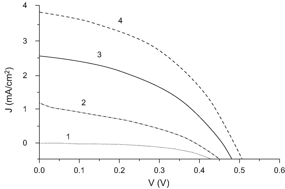
i–V curves of a ZnO/CdSe/CuSCN eta-solar cell. (1) Under dark conditions. (2) As-deposited CdSe. (3) Annealed CdSe. (4) Annealed CdSe 1 week later. Curves 2–4 are under illumination (340 W m–2).
Characteristic parameters of different ZnO/CdSe/CuSCN eta-solar cells
| Voc (mV) | Jsc (mA cm–2) | FF | Efficiency (%) | |
| As-deposited CdSe | 400 | 1.2 | 0.34 | 0.5 |
| Annealed CdSe | 460 | 2.6 | 0.42 | 1.5 |
| 490 | 3.9 | 0.42 | 2.3 |
Cells stored under vacuum (10–4 atm) for 24 h before gold contact deposition showed an improvement in FF, up to values of 0.50. This improvement is frequently correlated with a small decrease in Jsc, with no significant increase in conversion efficiency. Similar behavior was observed in n-type/dye/CuSCN cells by O'Regan et al. [17]. They attributed this increase in FF to evaporation of residual propylsulfide during vacuum storage.
The external quantum efficiency (eQE), the ratio of the number of charge carriers collected to the number of incident photons, of two cells is shown in Fig. 13. The wavelength range where the cells show the maximum eQE is in good correlation with the energy range of the solar spectrum where the flux is maximum. This confirms that the choice of CdSe as an absorber is judicious. We observed a significant improvement in eQE of cells with annealed CdSe. This indicates that the recombination effects are larger in cells with as-deposited CdSe, indicating the importance of large CdSe grain size in ZnO/CdSe/CuSCN eta-solar cells.

(a) External quantum efficiency of two ZnO/CdSe/CuSCN eta-solar cells. (b) Internal quantum efficiency of a ZnO/CdSe/CuSCN cell with annealed CdSe.
The internal quantum efficiency (iQE) was calculated, taking into account the total reflectance of the complete cell with annealed CdSe (Fig. 13). iQE refers to the efficiency with which light not transmitted through or reflected away from the cell generates charge carriers that can generate current. The obtained iQE, with a maximum around 28% and approximately square shape, is the best yet reported for inorganic eta-solar cells.
Complementary measurements were done under a Steuernagel solar simulator (AM 1.5) [14] at Energy Center of the Netherlands. These measurements were made 3 months after cell fabrication and under different illumination powers (0.1–1 sun). The energy conversion efficiencies measured there, ~1.5%, were similar to those found 2 months after the processing of the cell [37], confirming our previous measurements made without a solar simulator, showing the stability of the cells with time.
5 Summary and conclusions
A p–i–n nano-heterostructure was fabricated and physical properties of the various constituting layers were measured and analyzed, emphasizing the properties of interest for photovoltaic devices. A conformal and uniform coverage of the ZnO nanowires by CdSe, the absorber, has been obtained by electrodeposition, producing a very efficient light-trapping effect. The values of effective absorption (AE ~ 89%) and effective reflectance (RE ~ 8%) of the ZnO/CdSe/CuSCN heterostructure in the 400–800 nm of AM1.5 solar spectrum range, are very favorable for their use in photovoltaic devices. The ZnO/CdSe/CuSCN eta-solar cells have an internal quantum efficiency (iQE) with a maximum of 28%, the best reported for inorganic eta-solar cells. While this iQE is low compared with current values shown by Si solar cells, work on this and other eta-cells has still to be optimized.
A conversion efficiency of 1.5–2.3% was shown by the ZnO/CdSe/CuSCN eta-cells. This measured efficiency, joined with the easily accessible techniques used to make them, demonstrate that this nano-heterostructure in an interesting option to develop a ‘cheap’ technology to produce new solar cell devices. These cells exhibit characteristics similar to those of dye sensitized cells; the use of CdSe as absorber material in place of an organic or metallo-organic dye, should make for a cell with increased stability over time and allow a wider working temperature range.
The techniques used in fabricating these eta-solar cells have still to be optimized. Among the work to be done is optimization of the current density and/or potential at which CdSe is deposited, the thickness of the CdSe layer, annealing conditions for the CdSe layer, thickness of the top CuSCN layer, conditions for deposition of the gold contact layer, and methods for making the contact to the gold layer.
Acknowledgements
We are grateful to Brian O'Regan for numerous helpful discussions we had together.