1 Introduction
The so called eta-cell (eta: extremely thin absorber) is one of the alternative photovoltaic systems that has been developed during the last years, which makes use of highly structured surfaces [1]. In the eta-cell, the absorber layer is embedded between transparent electron and hole conductors [1]. Candidate materials to be used as transparent electron conductors are TiO2 [1] and ZnO [2] and for transparent hole conductors both inorganic (CuI [3], CuSCN [4] and CuAlO2 [5]) and organic (OMeTAD [6]) materials are still under investigation. For the absorber a large variety of compounds like semiconductor nanoparticles [7,8], CuInS2 [9,10] or CdTe [1] could be applied for assembling eta-cells. One of the main points in the development of these cell is the engineering of the electronic properties of the large electron conductor/absorber interface. In this way it has been shown that buffer layers of some metal oxides [11], In2S3 [10,12] or In(OH)xSy [13] improve the cell performance by decreasing recombination losses at the aforementioned interface.
In this work, a highly structured eta-cell such as TiO2/In(OH)xSy/PbS/PEDOT:PSS is presented. Porous TiO2 deposited on glass/SnO2:F substrate has been used as electron conductor and poly(3,4-ethylenedioxythiophene) doped with polystyrene sulfonic acid (PEDOT:PSS) has been chosen as hole conductor. Previous experiments carried out in our lab have shown that both buffer and absorber layers were needed in order to get photocurrent. Therefore thin films of In(OH)xSy [14] and PbS [15] both prepared by chemical bath deposition (CBD) were used as buffer and absorber layers respectively. Techniques like X-ray photoelectron spectroscopy (XPS), X-ray excited Auger electron spectroscopy (XAES), photovoltage (PV) spectroscopy, electron microscopy and photovoltaic response (current-voltage and quantum efficiency) were applied for the characterization of the layers and the corresponding solar cells.
2 Experimental
Highly structured TiO2 was deposited onto glass/SnO2:F substrates by spray pyrolysis [16]. In(OH)xSy was prepared by CBD from a solution containing InCl3, thioacetamide and different concentrations of hydrochloric acid (HCl) at 70 °C for 30 min following a procedure similar to one previously described [14]. For solar cell assembly, In(OH)xSy deposition was performed up to three times at 0.005 M HCl followed by a final annealing of the films in Ar atmosphere at 300 °C for 30 min. Afterwards PbS was prepared also by CBD following the conditions described by García et al. [15] from an aqueous solution containing Pb(CH3OOH)2, NaOH, triethaolamine, thiourea at 40 °C for 10 min. Undiluted PEDOT:PSS (Baytron P®) was deposited on top of In(OH)xSy / PbS layers by spin coating. The area of the solar cells was determined by evaporated back gold contacts of 0.03 cm2.
The morphology of the cells was studied by scanning electron microscopy (SEM). The composition of PbS layers was analyzed by XPS and XAES. PbS and In(OH)xSy layers were also characterized by photovoltage spectroscopy in the same set up recently described [17] and using a halogen lamp for generating the signal. Current-voltage measurements were performed in the dark and under illumination with a halogen lamp supplying 100 mW/cm2 power. The quantum efficiency was measured in a set-up which included a halogen lamp, a monochromator and a calibrated Si photodiode.
3 Results and Discussion
As said above, preliminary experiments carried out in our lab showed that for observing photovoltaic behaviour in devices containing PbS as absorber, the presence of a buffer layer of In(OH)xSy was necessary. In general it can be said that the role of the buffer in this kind of cells is to decrease the recombination probability at the interface absorber/electron conductor. In this way, In(OH)xSy has proved to be a good buffer for TiO2 solar cells [13]. One of the requirements of a buffer layer is to have a wide band gap in order to allow the light to reach the absorber. Therefore as a first stage In(OH)xSy films were deposited onto glass/SnO2:F using different amounts of HCl (i.e. at different pH-values) and photovoltage (PV) spectra were measured in order to obtain the optical band gap (Eg). Fig. 1 shows the dependence of Eg of CBD-In(OH)xSy thin films on the pH value for as deposited samples. As it can be seen, Eg of In(OH)xSy is about 2.4 eV for pH < 2.6 but, for higher pH-values, Eg increases up to about 3.4 eV (pH 3.0). In all cases Eg is high enough for CBD-In(OH)xSy to be a suitable buffer layer. The dependence of Eg on the pH value of the solution is most probably related to changes in the stoichiometry of In(OH)xSy. As reported in previous works, a higher content of sulphide is expected for lower pH values, whereas a higher content of hydroxide and/or oxide would be obtained for higher pH values [18]. This variation in the stoichiometry seems to be the origin of such Eg values [19], which are between the corresponding to both pure In2S3 (Eg = 2.0 eV [20]) and In2O3 (Eg = 3.7 eV [21,22]). After annealing in Ar at 300 °C, Eg for In(OH)xSy decreased from 2.4 eV to about 2.2 eV, which is an indication that hydroxide and oxide ions leave the CBD-In(OH)xSy thin films during the treatment. For further studies and preparation of eta-cells, CBD-In(OH)xSy buffer layers were deposited from solutions containing 0.005 M HCl (pH of 2.4) up to three times and subsequently annealed in Ar for 30 min.
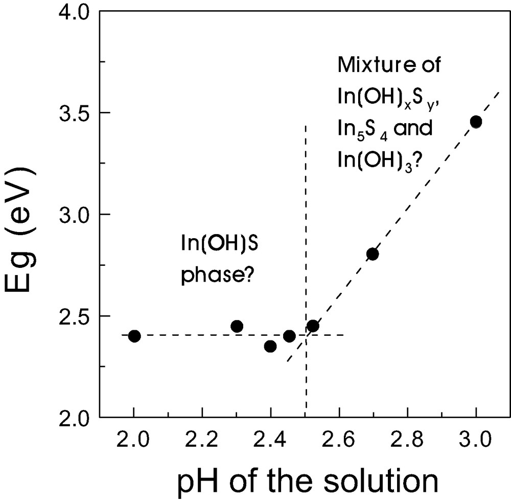
Dependence of the optical band gap (Eg) as determined by photovoltage spectroscopy of a prepared CBD-In(OH)xSy on the pH value of the solution.
Information about the chemical bonding in PbS prepared by CBD was obtained by XPS and XAES. For this purpose, the CBD-PbS layer was deposited on a glass/SnO2:F substrate. Fig. 2 shows the Pb NOO Auger signal in which a contribution of Auger electrons from at least two different Pb compounds, PbS and PbO (or Pb(OH)2), can be observed. This has been also confirmed by the XPS peak of Pb 4f7/2 emission (not shown here). From this peak the composition of the CBD-PbS absorber could be estimated revealing a PbO / PbS ratio of around 1.0 / 3.8, which indicates that CBD-PbS is more likely PbOZS1–Z with Z ≈ 0.21.
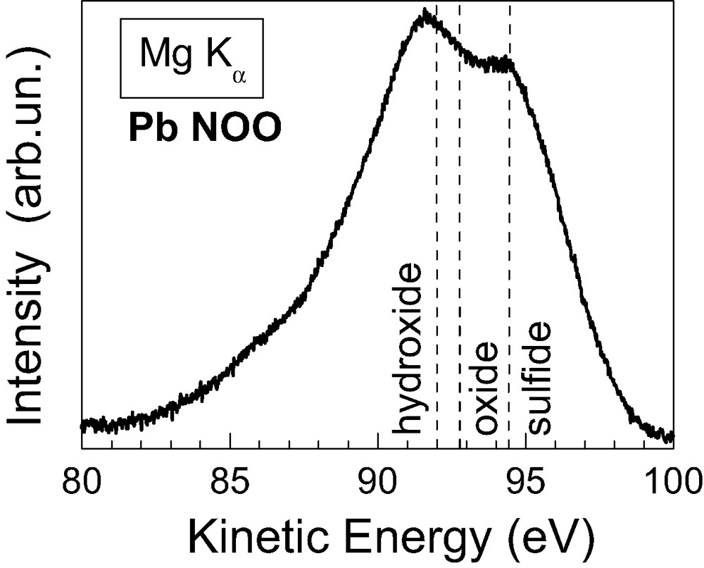
Pb NOO Auger spectrum of the PbS/SnO2:F/glass test structure. The reference positions for the Pb N6O45O45 Auger line of Pb(OH)2, PbO and PbS are also shown.
Photovoltage (PV) spectroscopy was performed in order to obtain information about the absorption edge of the materials. With this technique the voltage generated at the surface of a semiconducting material upon illumination is measured. Hence it gives an indication of the spatial separation of photogenerated electron-hole pairs when the absorption of photons occurs. Fig. 3 compares photovoltage spectra of highly structured TiO2 after deposition of In(OH)xSy (a), PbS (b) and In(OH)xSy/PbS (c). In all cases In(OH)xSy layers were annealed in Ar at 300 °C for 30 min. From this figure the values of Eg can be estimated for both annealed-In(OH)xSy (a) and PbS (b). For the first one a value of 2.2 eV is obtained and for the second one Eg amounts to about 0.85 eV. We can see the band gap of the CBD-PbS is widened in comparison to the value corresponding to the bulk PbS (Eg = 0.37 eV [23]). This widening of Eg can be mainly attributed to the composition of the CBD-PbS as the values of Eg found for PbO are 1.9 [24] and 2.8 [25] eV for the tetragonal and orthorhombic phases respectively. It is interesting to note that Eg of PbS is 0.85 eV for both the layer deposited onto TiO2 and onto In(OH)xSy. Therefore, the formation of a mixed InPbx(OH)ySz phase due to an ion exchange mechanism seems unlikely for the given preparation procedure. In Fig. 3c, it can also be observed that no photovoltage is obtained for energies higher than 2.4 eV, which could be due to a charge recombination at the interface of both In(OH)xSy and PbS.
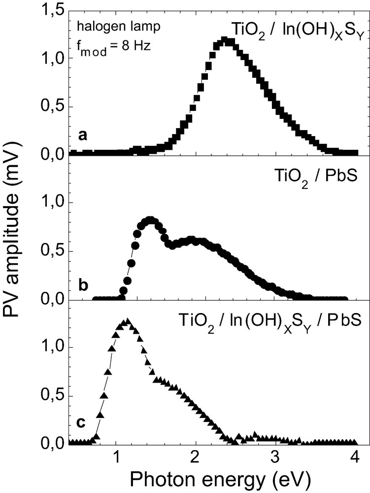
Photovoltage spectra amplitude of highly structured TiO2 after deposition of In(OH)xSy (a), PbS (b) and PbS/In(OH)xSy (c) thin films.
Fig. 4 shows an SEM cross section of a typical glass/SnO2:F/TiO2/In(OH)xSy/PbS/PEDOT:PSS/Au structure. We can see that TiO2 prepared by spray pyrolysis is highly structured with pores in the order of μm, which favours a good light scattering. Unfortunately it can also be seen that pores close to the SnO2:F front-contact are nearly empty, i.e. neither In(OH)xSy, PbS nor PEDOT:PSS have completely penetrated inside.
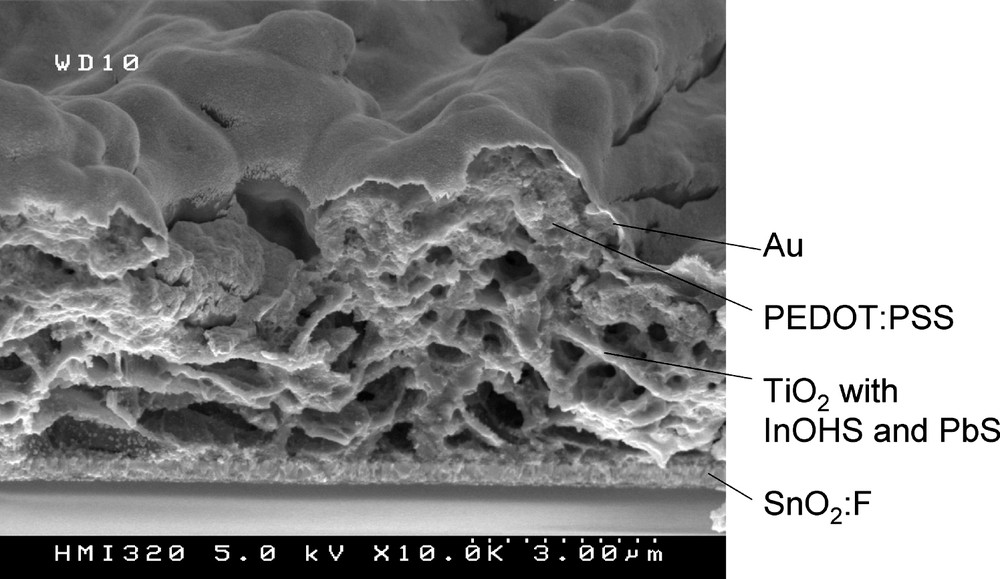
SEM cross section of a typical glass/SnO2:F/TiO2/In(OH)xSy/PbS/PEDOT:PSS/Au structure.
The performance of solar cells based on glass/SnO2:F/TiO2/In(OH)xSy/PbS/ PEDOT:PSS/Au structures was well reproducible. Fig. 5 shows current-voltage characteristics of a solar cell in the dark and under illumination. The rectifying behaviour of the cell looks quite good, the open circuit voltage and the short circuit current being 0.28 V and 7.4 mA/cm2, respectively. The efficiency of the given cell is 0.83% and the fill factor amounts to 0.4, which is relatively good in comparison to previously reported results for eta-cells [16]. The high series resistance seems to be the main problem for getting high efficiencies at the present stage. To our opinion, the performance of such solar cells could be improved if the structural properties of the cell are improved, which should come through an optimisation of the deposition methods for the materials.
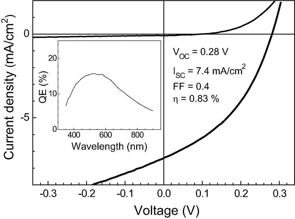
Current-voltage characteristics in the dark and under illumination (100 mW/cm2) of a TiO2/In(OH)xSy/PbS/PEDOT:PSS/Au solar cell. Inset: spectral dependence of the external quantum efficiency.
Fig. 5 (inset) shows the spectral dependence of the external quantum efficiency (QE) of the corresponding cell measured between 1.37 and 3.55 eV. We can see that in the region of absorption of PbS, the QE increases from 5% to 13% reaching a maximum of 16% at about 2.3 eV. It is interesting to note that QE attains the highest values in the region where there is almost no photovoltage signal (see Fig. 3c). This shows that the injection of electrons into TiO2 and holes into PEDOT:PSS are both important and that the PEDOT:PSS layer has a strong influence on the behaviour of the charge separation and injection processes in the solar cell.
4 Conclusions
This is the first time a solid state cell based on highly structured TiO2/In(OH)xSy/PbS/PEDOT:PSS with efficiency close to 1% has been developed. In such device both In(OH)xSy buffer and PbS absorber layer play crucial roles. The main limitations of these cells are the low Voc obtained (only 0.3 V) and the low penetration of the materials (specially PEDOT:PSS) inside the TiO2 pores. Specific questions such as the influence of the layer structure and the interfaces on the charge separation remain unclear and should be considered in future investigations. The optimisation of the whole cell assembly in terms of deposition techniques of all the components (specially for improving the penetration in the pores) must be the main concern if higher efficiencies want to be obtained.
Acknowledgements
The authors are grateful to the European Comission (A. B., HPRN-CT-2000-00141) and to the ‘Deutscher akademischer Austauschdienst’ (Robinson Musembi fellowship) for the financial support and to I. Sieber for the electron-microscopy micrographs.


