

1 Introduction
Titanium dioxide (TiO2) is intensively studied because of its potential applications in various fields such as: liquid and solid nanostructured solar cells, with inorganic or organic extremely thin absorbers [1–4]. Furthermore, TiO2 was investigated for catalysis and in electrochromic devices [5–7]. In the literature, several reports have recently appeared on TiO2 thin films obtained by different techniques. Spray pyrolysis method has been employed to deposit TiO2 thin film using titanium (IV) oxy-acetylacetonate 2-butanol solution with substrate temperature between 300 and 500 °C by Okuya et al. [8] and used for dye-sensitized solar cells. Karunagaran et al. [9] have used DC magnetron sputtering method to deposit TiO2 films onto the Si-substrates and obtained mixture of anatase and rutile phases. Superionic cluster beams produced by pulsed micro-plasma cluster source have been used to prepare nanocrystalline thin films of TiO2 by Taurino et al. [10]. Fang and Chen [11] used TiCl4 in n-propanol to prepare Titania particles by thermal hydrolysis method. Spin-coating method has been used to deposit TiO2 thin films using ammonium titanyl oxalate in aqueous solution [12]. Gao et al. [13] have used aqueous peroxotitanate solution at room temperature to deposit amorphous and nanometer sized TiO2 thin films. Vigil et al. [14] have used microwave radiation heating to activate a flow of Titania precursor, which leads to the deposition of TiO2 layers. Recently, Vigil et al. [15] have used microwave chemical bath deposition method for the deposition of TiO2 thin films. Oekermann et al. [16] studied electron transport and back reaction with nanocrystalline TiO2 films prepared by hydrothermal crystallization. Natarajan and Nagami [17] have reported cathodic electrodeposition of nanocrystalline TiO2 thin films using Ti powder with H2O2 and ammonia. Karuppuchamy et al. [18] have modified this process. They used TiOSO4 with H2O2 for the electrodeposition of TiO2 thin films.
Due to the demands of TiO2 in different applications, simple and low cost techniques are required for thin film deposition. Chemical and electrochemical methods are emerging as important synthetic methods to thin films not only for their cost effectiveness but also for the high quality of the materials. These methods are suitable for large area and even for complex structures. In the present investigation, we report on the chemical and electrochemical synthesis of nanocrystalline TiO2 anatase thin films and powder. Characterizations were accomplished by using various techniques such as XRD, TEM, XPS, SEM, and AFM.
2 Experimental
All the chemicals are of highest purity (99.99%) and commercially available. They were used without further purification. Glass, commercially available indium tin oxide (ITO) coated glass (10 Ω/cm2, Präzisions Glas and Optik GmbH, Germany) and quartz were used as substrates. Prior to the deposition the substrates were ultrasonically cleaned with acetone, ethanol and detergent and finally with ultra pure water.
2.1 Chemical synthesis
Aqueous solution was prepared by mixing 0.8 g of the titanium oxide sulfate (TiOSO4) (Sigma-Aldrich Grade) and 2 ml H2O2 (30%) (Merck Grade) followed by 50 ml water in a beaker of capacity 100 ml. The obtained mixture was colloidal with pH ~2. The solution was initially orange/turbid and turned to clear red solution under constant stirring after 25 min at room temperature.
Deposition was carried out by vertical immersion of the substrates in the solution with continuous stirring. The substrates were withdrawn from the solution after certain deposition time (6 h for ITO and 12 h for films deposited on glass and quartz). After rinsing with distilled water, the samples were dried with nitrogen at room temperature (25 °C). The ‘by-product’ powder was collected through filtering, washed, dried, and submitted for further characterization
2.2 Electrochemical synthesis
The precursor bath consisted of 0.04 M TiOSO4, 0.2 M H2O2 and 0.1 M KNO3 (pH ~ 2) solutions maintained at room temperature (25 °C) was used for electrochemical synthesis. The clear solution was used as electrolyte. A conventional three electrodes electrochemical cell was used for electrosynthesis. Saturated calomel electrode (SCE) was used as reference and all the potentials were quoted with respect to this reference. The counter and working electrodes were platinium and ITO coated glass, respectively. The deposition was carried out by applying –1.2 V potential vs. SCE for 3 h. During deposition, the bath solution was continuously stirred. Typically 3 h deposition resulted in a smooth and flat film with a thickness of 50 nm. As a result of hydrolysis white amorphous titanium oxyhydroxide gel particles were observed in the bath after 3 h. The formed gel powder in the bath was collected by filtering the solution.
The films and the byproducts were annealed in air at 400, 450 and 500 °C temperatures. It was observed that annealing at 500 °C for 1 h had better cystallinity than others. Annealing treatment allowed converting the amorphous film into anatase-phase. The annealing temperature of 500 °C was chosen for further studies.
2.3 Characterizations
X-ray diffraction (XRD) spectra were recorded with an automated Bruker D8 advance X-ray diffractometer with the following characteristics: Cu Kα, λ = 1.5406 Å, 40 kV, 40 mA and 2θ = 20–80°. Measurements for thin films were taken using a glancing angle detector at θ = 1°. Steps and collection time were, respectively, 0.01° and 7 s. The average crystallite size was determined with the Scherrer's method associated with the Topas 1.0 software. The phase composition was identified using the program EVA (version 4.0) provided by Bruker diffractometer.
Philips CM12 microscope operated at 120 kV was used for performing transmission electron microscopy (TEM). Axial illumination as well as the ‘nanoprobe mode’, with a beam spots size of 1.5 nm was used to identify diffraction of individual clusters. High-resolution (HRTEM) images were digitally recorded by using a CCD camera. XPS measurements were performed using a Leybold EA11 MCD spectrometer with an Mg Kα source at 1253.6 eV. The base pressure was 2 × 10⁻⁸ Pa. Peaks were fitted with Gauss–Lorentz shapes.
Scanning electron microscopy (SEM) images were recorded using a LEO1530 (Gemini) FE-SEM microscope with Schottky field emission and acceleration voltage of 10 kV. Atomic force microscopy (AFM) images were recorded using the Nanoscope IIIa scanning probe microscope in a contact mode. The commercial n+-silicon cantilevers were used with a typical spring constant of 0.2 N/m in order to investigate the surface roughness.
3 Results and discussion
3.1 Structural studies
TiO2 has three well-known phases namely: anatase, rutile, and brookite [5]. Rutile and anatase are tetragonal whereas brookite is orthorhombic. Rutile is the only stable phase. Anatase and brookite are metastable at all temperatures, and can be converted to rutile after heat treatment at high temperature. Fig. 1 shows XRD pattern of TiO2 films deposited on ITO substrates by chemical (Fig. 1b) and electrochemical (Fig. 1c) method. ITO substrate was used as a reference (Fig. 1a). The most intense (101) peak of the TiO2 in the X-ray pattern (Fig. 1b) for chemical deposited film was observed at 2 θ = 25.3° with a full width of 0.25° at a half-maximum intensity along with tiny peaks of (220) and (105) planes. This is an indication of interference-free reflection of the typical tetragonal-anatase as compared to standard JCPDS data [19]. Obviously XRD patterns do not shows any rutile or brookite peaks. Similar crystal structure was observed for electrodeposited films on ITO and chemically deposited films on glass and quartz substrates (see Fig. 2a, b). We observed that low deposition rate was favored for the films on glass and quartz substrates hence the deposition was performed for 12 h in order to get thicker films for structural analysis. Furthermore, the collected byproduct from chemical bath showed polycrystalline nature with preferred orientation along (101) plane with anatase structure (see Fig. 2c). Using Scherrer's formula, we evaluated the crystallites size along (101) orientation. We obtained 16, 24 and 23 nm, respectively, for the films on ITO, glass, and quartz substrates, respectively, for chemically deposited films. The crystallite size for collected powder was 17 nm. Crystallite size of 23 nm was estimated for electrodeposited films.

X-ray diffraction patterns of (a) ITO (as reference) and TiO2 films deposited by (b) chemical and (c) electrochemical methods on ITO substrate followed by annealing at 500 °C for 1 h in air.
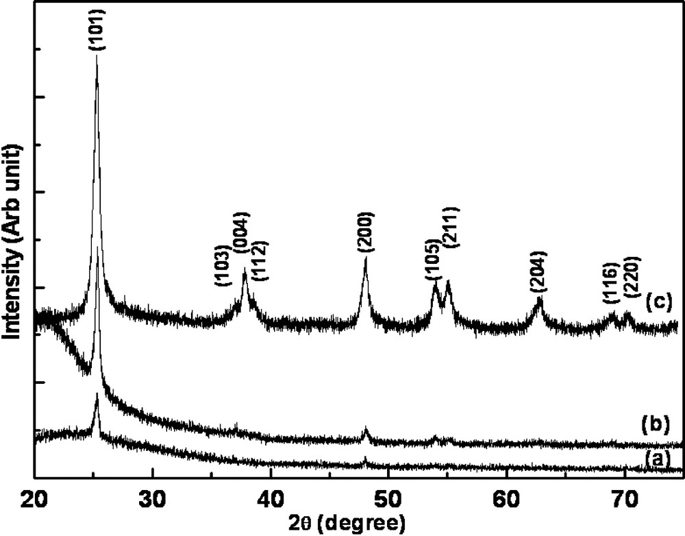
X-ray diffraction patterns of chemically deposited TiO2 thin films annealed at 500 °C for 1 h in air on (a) the glass substrate (b) the quartz substrate and (c) the collected byproduct annealed at 500 °C for 1 h in air.
Figs. 3 and 4a show transmission electron micrographs of the TiO2 film deposited by chemical and electrochemical methods on glass and ITO substrates, respectively. The images exhibited a spherical and elongated shaped particles with roughly uniform in size of about 20–30 nm. High-resolution TEM images shows clearly developed lattice feature (Figs. 3 and 4b) which indicates that each of these larger particles is an agglomeration of smaller particles, with nanostructured domain. Fourier transformation (Figs. 3 and 4c) leads to demonstrate the inter-planer distance (d-spacing) of 3.59 and 3.45 Å for chemically and electrochemically deposited films, respectively. Comparing d-spacing with standard JCPDS data, we conclude that the anatase-phase with specific orientation along (101) direction was observed [19].

(a) Inset shows TEM image of the TiO2 film deposited by chemical method followed by annealing at 500 °C for 1 h in air. (b) A high-resolution image of a portion of the investigated image in (a). Results obtained after Fourier transformation of the high-resolution image is as shown in (c).
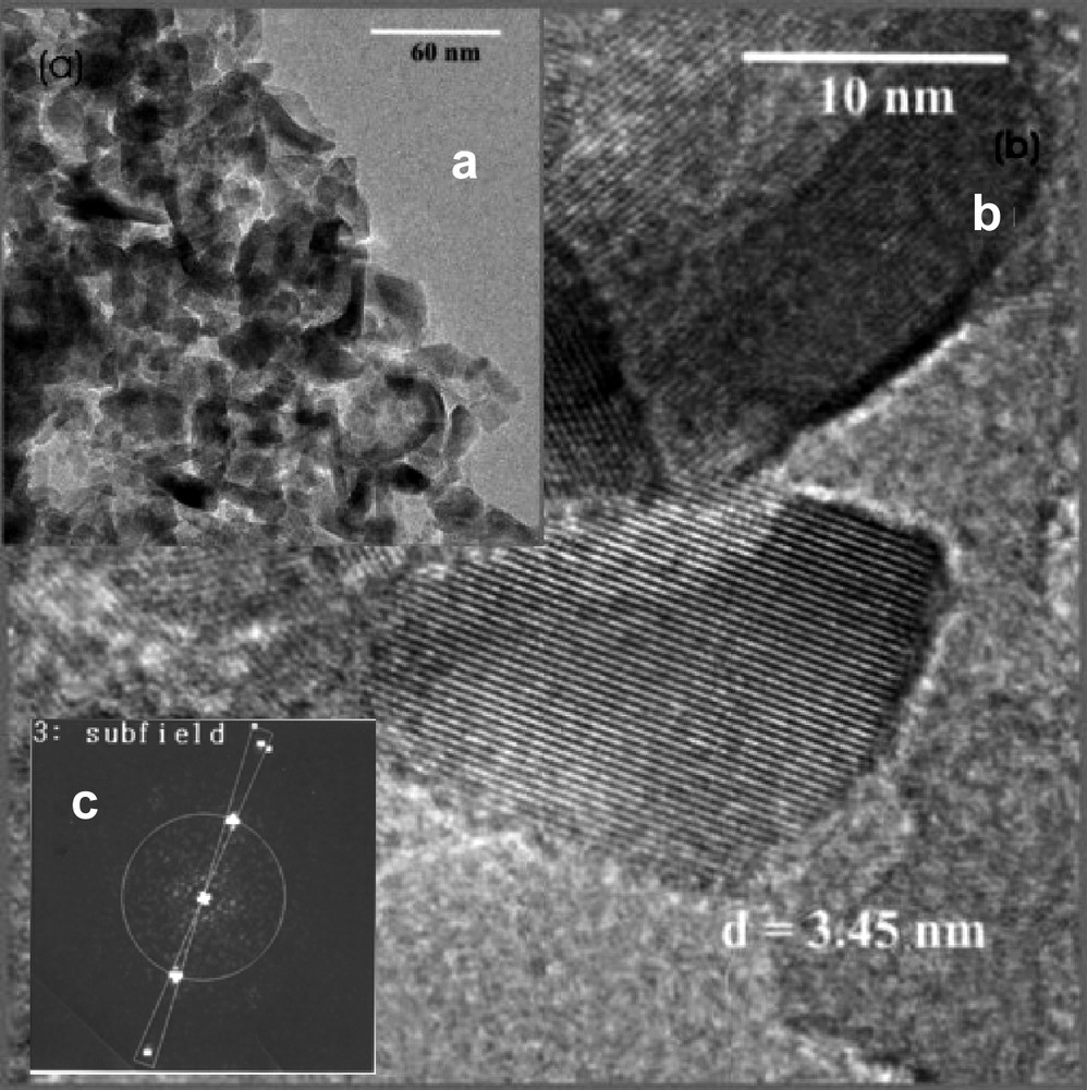
(a) Inset shows TEM image of the TiO2 film deposited by electrochemical method followed by annealing at 500 °C for 1 h in air. (b) A high-resolution image of a portion of the investigated image in (a). Results obtained after Fourier transformation of the high-resolution image is as shown in (c).
3.2 XPS measurements
XPS measurement was performed for chemically deposited films. Fig. 5a shows the XPS survey spectra of the TiO2 film deposited on the ITO substrate. Major characteristic transition peaks for Ti, O and C are indicated. The 2p3/2 peak for Ti has a binding energy of 453.8 eV for metal, 455.1 for TiO, 458.5 for TiO2 while 459.2 for anatase/rutile TiO2 [20]. The high-resolution scan (inset in Fig. 5b) showed that the photoelectron peak for Ti at 459.5 eV, which is in the form of TiO2, corresponds to anatase-phase, also supported by structural studies. In the present case, we observed that the O1s peak was composed of two peaks revealing the presence of two forms of oxygen (inset Fig. 5c). The analysis by deconvolution shows two peaks at 530.8 and 533.2 eV. The major peak at 530.8 eV well matched with 530.1 eV for TiO2 [20]. The minor peak might be due to the oxygen from the surface contamination, which is common for chemical deposited films. Also, some part of oxygen bonded with hydrogen cannot be excluded in the present case [20]. In addition to that, contamination of the surface by carbon is evident as peak for this element is already visible at 285.8 eV for the virgin TiO2 surface [21].
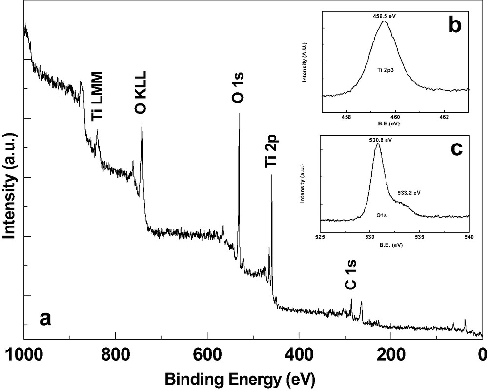
(a) Elemental XPS spectra of the TiO2 film by chemical method followed by annealing at 500 °C for 1 h in air. Insets (b) and (c) show high-resolution scans for Ti2p3 and O1s, respectively.
3.3 Surface morphology
SEM images of TiO2 on ITO substrate deposited by (a) chemical and (b) electrochemical methods are shown in Fig. 6. Small grains with dense structure and well surface coverage are observed for chemically deposited film. SEM cross-section of the TiO2 film (see inset) shows compact film with a thickness around 20 nm. For electrochemically deposited films, a conformal coverage of the ITO substrate without any cracks or holes was obvious. The electrodeposited film is compact with a thickness of 50 nm as estimated by cross-sectional analysis (see inset).

SEM images of the TiO2 films deposited by (a) chemical and (b) electrochemical methods followed by annealing at 500 °C for 1 h in air. Inset is the cross-section images, shows the compactness of the films.
AFM studies in contact mode were performed for TiO2 film deposited by (a) chemical and (b) electrochemical methods on the ITO substrates (see Fig. 7). The films were dense and compact. Evaluation of surface patterns was conducted by estimating the roughness of the film (root-mean-squared). The root-mean-square (r.m.s.) roughnesses of 9 and 10 nm were evaluated from 9 μm2 surface area for chemical and electrochemical deposited films, respectively.

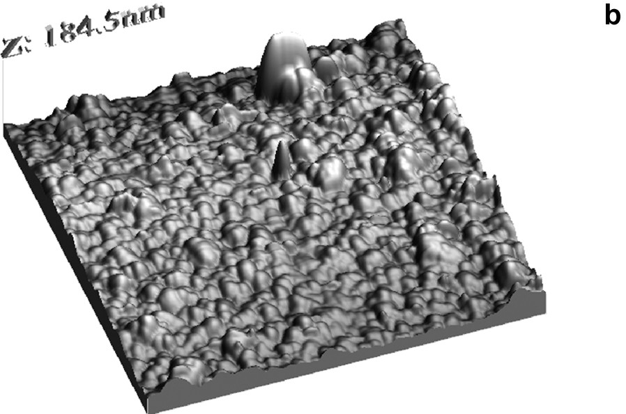
Surface view AFM image of the TiO2 films deposited by (a) chemical method and (b) electrochemical method followed by annealing at 500 °C for 1 h in air.
4 Conclusions
Chemical and electrochemical methods have been successfully used for the synthesis of TiO2 thin films and powders as byproduct. Both chemical and electrochemical methods are simple and suitable for the preparation of large area TiO2 anatase films by one step process. Air-annealing at 500 °C of as deposited amorphous films leads to the formation of anatase-phase. The annealed byproducts showed TiO2 anatase structure as well. The dense, uniform and compact films on ITO substrates were observed by surface morphological studies. Nanocrystallites consisting of agglomerations of small particles are revealed by TEM and HRTEM analysis.
Acknowledgements
One of the authors S.D.S. acknowledges to Alexander von Humboldt (AvH), Foundation, Germany, for the financial support.