

1 Introduction
Within the last decade, nanoscience has reached the status of a leading science with fundamental and applied implications in all basic physical, life, and earth sciences as well as engineering and materials sciences. An important feature of nanoscience is that it bridges the crucial dimensional gap between the atomic and molecular scale of fundamental sciences and the microstructural scale of engineering and manufacturing. Accordingly, a vast amount of true multidisciplinary fundamental knowledge is currently being explored and linked. It will lead to a tremendous amount of new in-depth understanding as well as to the fabrication of novel high technological devices in many fields of applications from electronics to medicine [1]. The important basic goals have been to develop various synthetic techniques to produce large quantity of building blocks of low dimensionality (zero- and one-dimension) in a controllable and fashionable way. The crucial challenge remaining for scientists and engineers is to develop the ability and competence to hierarchically order, connect, and integrate quantum dots [2], nanorods and nanowires [3], nanobelts and nanosaws [4] as well as nanotubes [5] in functional network, thin film coatings, and three-dimensional (3-D) arrays to generate and manufacture practical nanodevices. These future devices based on such advanced building blocks should revolutionize the industry [6] and the economy given that they possess the unique properties of nanoscale as well as the ability to connect the nanoworld to the microworld.
In this regard, our strategy to generate large-area of advanced nano and micro-particulate thin films at low cost is a bottom-up aqueous chemical growth approach (Fig. 1) [7] that is well-resourced by a classical thermodynamic model, monitoring the nucleation, growth, and aging processes via the experimental control of the interfacial free energy of the system [8]. Such a strategy has been well-illustrated on the size control of magnetite nanoparticles over an order of magnitude [9]. This concept and synthetic method allows the design and the creation of metal oxide nanomaterials with novel morphology, texture, and orientation which enables to probe, tune, and optimize their physical properties [10]. Particulate thin films and 3-D arrays are obtained by direct growth onto various substrates from the condensation of aqueous precursors at low temperatures. Such an approach to material synthesis offers the ability to generate anisotropic nanoparticles and to control their orientation onto substrates. Such an approach has been successfully applied for the growth of advanced nano- and micro- particulate metal oxide materials such as three-dimensional arrays of ferric oxide nanorods [11] for photovoltaic [12] and photocatalytic applications [13], nanocomposite arrays of iron and chromium corundum sesquioxides [14] as well as nanorod [15], microrod [16] and microtube [17] oriented arrays of zinc oxide for photovoltaic and optoelectronic devices. Ferromagnetic 3-D array of metallic iron nanorods for magnetic devices [18], 2-D arrays of chromium oxide [19] for non-linear optics and magnetoelectrics applications, 3-D oriented arrays of tin dioxide nanorods with square cross section [20] for gas sensing and photocatalytic applications as well as large specific area bio-inorganic arrays for bio-sensors [21] have also been fabricated by such a method. In addition to developing functional materials for various applications, growing such large nanostructured arrays with well-controlled orientation and morphology allows experimental probing and characterization of well-defined nano- to micro-structures [22]. Consequently, a direct feedback between theoretical calculations and experimental data [23] contributes to the improvement and optimization of existing devices as well as to a better fundamental knowledge of their physical/chemical and structural properties as well as their electronic structure [24].

The controlled aqueous chemical growth thin film growth technique: immersion of substrates in aqueous solutions of metal salt precursors (left), heat treatment in a conventional laboratory oven below 100 °C (center) and generation of nano-, meso-, and micro-particulate thin films of large (i.e. several tens of cm2) physical surface area (right).
Our work focuses most exclusively on metal oxides, because they represent the most common, most diverse, and richest class of materials in terms of electronic structure and physical, chemical, and structural properties. Such properties include for instance, optical, optoelectronic, magnetic, electrical, thermal, photoelectrochemical, photovoltaic, mechanical, and catalytic ones. As a result, numerous applications of metal oxides such as ceramics (chemical-, gas-, and bio-) sensors, actuators, lasers, waveguides, IR, UV and solar absorbers, pigments, photodetectors, optical switches, photochromics, refractors, electrochromics (electro- and photo-)catalysts and support for catalysts, insulators, semiconductors, superconductors, supercapacitors, transistors, varistors, resonators, dielectrics, piezoelectrics, pyroelectrics, ferroelectrics, magnets, transducers, thermistors, thermoelectrics, protective and anticorrosion coatings, fuel cells, anode and cathode materials for alkaline and lithium batteries, and solar cells have been developed. The diversity of such applications originates from the more complex crystal and electronic structures of metal oxides compared to other class of materials. The main reasons are related to their variety of oxidation states, coordination number, symmetry, ligand-field stabilization, density, stoichiometry and acid–base properties, which yield fascinating compounds exhibiting insulating, semiconducting, conducting, or magnetic behaviors with transitions among those states. The combinations of such variety of distinctive properties and applications with the unique effects of low dimensionality at nanoscale make the development of metal oxide nanostructures an important challenge from both fundamental and industrial standpoints.
One of the major challenges facing the much anticipated, broader commercial realization of devices emerging from nanotechnology is the economical manufacturing of reliable and practical nanostructures with tailored properties. The preparation of functional nanomaterials of well-defined morphology aims to improve the efficiency of existing devices as well as developing novel well-designed and innovative devices. Modeling of such structures by simulation/calculation methods [25] would allow a better understanding of size effect [26] and structure–efficiency relationships. Based on fundamental knowledge, new and/or improved semiconductor materials and devices are developed to increase the performance, e.g. efficiency, sensitivity, selectivity, and reliability, of semiconductor devices while keeping their fabrication at low cost to meet the market demand. For instance, the controlled growth and orientation of nano-, meso- and micro-structures along preferred crystal directions, e.g. highest electronic density, as well as designated pathway will enable a more efficient separation of photogenerated carriers and a better electron transport in photoelectrochemical devices. This paper intends to illustrate the latest advances in the development of large-bandgap semiconductor thin film materials of novel texture and morphology by the low cost and environmental-friendly fabrication and manufacturing of nanoengineered arrays of transition and post-transition metal oxides.
2 Approach
A new approach to semiconductor materials design is proposed. The application of a novel low temperature aqueous chemistry technique to produce large-area nanoparticle arrays and nanoparticulate thin films directly onto various types of substrate (e.g., transparent conductive oxide (TCO), Si wafers, sapphire, polypropylene, glass etc.) is used to produce a new generation of functional materials for photovoltaic and photocatalytic applications. Such a chemical growth technique is capable of producing metal oxide building blocks of various morphologies, sizes, and orientations including oriented one-dimensional materials such as nanorods and nanowires that are of interest for semiconductor technology, such as for instance SnO2, ZnO, WO3, α-Fe2O3, α-Cr2O3, Co3O4, and Mn3O4. We have demonstrated that these purpose-built nanomaterials can be generated on several types of substrates; they can be patterned using a variety of techniques [27]; and large physical areas can be easily formed. Thus, these materials can be readily exploited as photoanodes for photovoltaics, photocatalysts, as well as for sensors. Such ordered purpose-built nanomaterials are obtained by a novel synthesis and theoretical concept which consists of growing metal oxide thin films directly onto substrates at precipitation and dispersion conditions yielding to thermodynamic colloidal stability (i.e. low interfacial tension). Such specific state is reached by monitoring experimentally (i.e. chemically and electrostatically) the interfacial tension of the system as described quantitatively by a thermodynamic model based on Gibbs adsorption equation [8].
2.1 Dimensional control
The main idea is to tune the thermodynamics and kinetics of nucleation, growth, and ageing of a system by controlling experimentally its interfacial tension. For instance, the ability to segregate the nucleation and the growth stage enables to control the monodispersity of nanoparticles. Indeed, performing an aqueous precipitation far from the typical point of zero charge (PZC) of the investigated metal oxide allows an enhanced control of the nucleation, growth, and ageing processes. Considering acid–base properties of metal oxide surfaces, increasing (or decreasing) the pH of precipitation/dispersion from the PZC will increase the surface charge density by adsorption of hydroxyl ions (or protons). Consequently, the chemical composition of the interface will change, and so the interfacial tension of the system. In addition, a high ionic strength will contribute to a further increase of the surface charge density. This is understood by considering the electrostatic forces at the interface; indeed by increasing the ionic strength of the medium, a more effective screening effect of the interfacial charged sites will allow further surface sites to develop a charge. In such case, the surface charge may therefore reach its maximum charge density, which ultimately depends on the oxygen structure and composition of the interface. At maximum charge density, the interfacial tension of the system will reach a minimum. Thermodynamic colloidal stability may thus be reached resulting in a considerable lowering of the secondary ageing processes, henceforth preventing the nanoparticle size and its distribution to increase as well as avoiding crystal phase and morphological transformations.
Any adsorption phenomenon at interface decreases the surface (or interfacial) tension γ. Such effect is described quantitatively by the Gibbs adsorption equation:
| (1) |
| (2) |
| (3) |
For precipitation occurring between the PZC and the point of zero interfacial tension (PZIT), the surface charge does not reach its maximum, and consequently the interfacial tension remains positive and the system is submitted to secondary growth and ageing. As a result, the nanoparticles will evolve in solution, that is, their size will increase with time, and their crystal structure may be subjected to phase transformations. This is the unstable region of the precipitation. However, at precipitation pH ≥ PZIT, i.e. the stable region, the nanoparticles are thermodynamically stabilized, and consequently secondary growth phenomenon such as Ostwald ripening does not occur. No longer submitted to ageing, the nanoparticle size is finite and is directly related to the precipitation conditions such as pH and ionic strength at a given temperature and precursor concentration.
By consideration of the nucleation and growth processes which rule the generation of solid phases from solutions, a maximum is found for the first derivative of the free enthalpy of nucleation, the nucleation energy barrier, with respect to the number of precursors (which essentially represents the particle size). Such a maximum depends on the interfacial tension at the cubic power:
| (4) |
Therefore, reducing the interfacial tension leads to an important lowering of the nucleation energy barrier, which in turn leads to the decrease of the nanoparticle size. A large stage of nucleation of very small particle accompanied by a very short stage of growth is predicted. As a result, the average nanoparticle size (and its distribution) is expected to decrease substantially.
The experimental corroboration of such concepts was performed on the controlled aqueous precipitation of crystalline magnetite (Fe3O4) nanoparticles at room temperature. It clearly illustrated that the thermodynamic stability of metal oxide nanoparticles is a reality. It also demonstrated that the average particle size may experimentally be monitored (and semi-empirically predicted) over an order of magnitude from 1.5 to 15 nm with narrow size distributions. The excellent agreement between theory and experiments sustained the accuracy and relevance of the general and efficient growth control concepts of metal oxide nanoparticles under low interfacial tension conditions. Moreover, such conclusions entitled great expectations for a future development of advanced particulate nanomaterials devices with tailored and optimized physical/chemical properties.
In summary, the strict monitoring of the precipitation conditions during the entire synthesis yields to a very simple, yet efficient, control of the nanoparticle size and its distribution in solution.
2.2 Morphological control
Moreover, when the thermodynamic stabilization is achieved, not only the size is tailored but also the shape as well as the crystallographic structure may be controlled. For instance, at low interfacial tension, the shape of nanoparticles does not necessarily require being spherical; indeed very often nanoparticles develop a spherical morphology to minimize their surface energy because the sphere represents the smallest surface for a given volume. However, if the synthesis and dispersion conditions are suitable (i.e. yielding to the thermodynamic stabilization of the system), the shape of the crystallites will be driven by the symmetry of the crystal structure as well as by the chemical environment, and various morphologies may therefore be developed. Manipulating and controlling the interfacial tension enables to grow nanoparticles with sizes and shapes tailored for their applications. Applying the appropriate solution chemistry (precursors and precipitation/dispersion conditions) to the investigated transition metal ion along with the natural crystal symmetry and anisotropy or by forcing the material to grow along a certain crystallographic direction by controlling chemically the specific interfacial adsorptions of ions and/or ligand and crystal-filed stabilization, one can reach the ability to develop purpose-built crystal morphology.
2.3 Orientation control
To develop the capability of growing nano- to micro-particulate thin films from aqueous solution and controlling the orientation of large arrays of anisotropic nanoparticles onto a substrate, one has to consider the differences between homogeneous and heterogeneous nucleation phenomena. In most cases, homogenous nucleation of solid phases from solutions requires a higher activation energy barrier and therefore, heteronucleation is promoted and energetically more favorable. Indeed, the interfacial energy between two solids is generally smaller than the interfacial energy between a solid and a solution, and therefore nucleation may take place at a lower saturation ratio onto a substrate than in solution. Nuclei will grow by heteronucleation onto the substrate and various morphologies and orientation monitoring can be obtained by experimental control of the chemical composition of the precipitation medium. To illustrate and demonstrate such capabilities, the example of an anisotropic crystal is taken and the possibilities of experimentally monitoring its orientations onto a substrate using the aqueous chemical growth thin film processing technique are exposed hereafter.
Anisotropic building blocks with multi-angular orientation onto substrates may be generated when the number of nuclei is exceedingly limited by the precipitation conditions (through the chemical and electrostatic monitoring of the interfacial tension). The system will promote twinning and the preferential epitaxial three-dimensional growth of the rods along their easy axis from a very limited number of nuclei will induce star/flower-shape morphologies.
Anisotropic building blocks with a perpendicular orientation onto substrates may be obtained when the number of nuclei is slightly limited by the precipitation conditions. The slow appearance of a limited number of nuclei will allow the slow growth (according to the crystal symmetry and relative face velocities) along the easy direction of crystallization. As a result, a condensed phase of anisotropic nanorods parallel to the substrate normal will be generated.
Anisotropic building blocks with a parallel orientation onto substrates can be obtained when the nucleation rate is enhanced by the precipitation conditions. Indeed, the fast appearance of a large number of nuclei will result in a rapid two-dimensional growth. The stacking of anisotropic nanoparticles with random orientation between each other but with an overall perpendicular orientation with respect to the substrate normal is therefore promoted.
The ability to design materials consisting of anisotropic nanoparticles of different orientations enables the experimental studies of the angular dependence influences on the physical/chemical properties and electronic structure of materials and gives further opportunities for materials design and engineering (e.g. increased dimensionality).
2.4 Structural control
In addition to the control of particle size, shape, and orientation, precipitation of nanoparticles at low interfacial tension allows the stabilization of oxide and oxyhydroxide metastable crystal structures. Crystal phase transitions in solution generally operate through a dissolution-recrystallization process to comply with the surface energy minimization requirement of the system. Indeed, when a solid offers several allotropic phases and polymorphs, it is typically the one with the highest solubility and consequently the lowest stability (i.e. the crystallographic metastable phase), which precipitates first. This is understood by considering the nucleation kinetics of the solids. At a given supersaturation ratio, the germ size is as small (and the nucleation rate as high) as the interfacial tension of the system is low. Thus, given that the solubility is inversely proportional to the interfacial tension, the precipitation of the most soluble phase and consequently the less stable thermodynamically, is therefore kinetically promoted. Due to its solubility and metastability, this particular phase is more sensitive to secondary growth and ageing, which leads to crystallographically more stable phases, essentially by heteronucleation. Secondary growth and ageing processes are delicate to control and the phase transformations appear within a few hours to a few days in solution, whence the resulting undesired mixing of allotropic phases and polymorphs. However, by careful consideration of the precipitation conditions (i.e. at thermodynamically stable conditions), such phenomena may be avoided when nanosystems are precipitated at low interfacial tension. In summary, by adjusting the experimental conditions to reach the thermodynamic stability of a system, the nanoparticle size, shape, and crystal structure may be tuned and optimized. It allows the functionalized design of nanomaterials and the ability to quantitatively probe the influence of such parameters on the physical and chemical properties of metal oxide nanoparticles and nanoparticulate materials.
The outcome allows the fabrication of innovative and functional nano- to micro-particulate thin films of metal oxides directly onto substrates without membrane, template, surfactant, undercoating or applied external fields. Such purpose-built nanomaterials are prepared in such a way that particle nucleation is separated from growth, giving exquisite control of particle size. In many cases, the differences between interfacial energies among crystal facets can be exploited to produce controlled anisotropic shapes. In addition, since the purpose-built nanomaterials are fabricated at low temperature and can be deposited on almost any substrate, it is possible to deposit one phase on another. This opens up the possibility of using the anisotropy of one material to generate a high surface area substrate upon which a second, active, material is deposited. In effect, this produces nanocomposites-materials combining properties and architectures from multiple phases to achieve results not available from any single phase.
Five distinctive purpose-built metal oxide-based systems are foreseen to substantially contribute to a new generation of photocatalytic, photovoltaic, and optoelectronic devices, i.e. ZnO, SnO2, WO3, α-Fe2O3 and spinel oxides.
3 Outcome and achievement
The latest developments in materials design of zinc oxide, tin dioxide, and iron sesquioxide are illustrated in the following sections.
3.1 ZnO
II–VI large bandgap semiconductor, ZnO is well known and extensively studied for gas sensors, optoelectronics such as nanolasers [28] and field emission devices [29] as well as UV absorber and photoanodes for photovoltaics and dye sensitized solar cells [30]. Zinc oxide is a great example of the capability of low temperature aqueous chemical growth to design, onto many different kinds of substrates, various ordered architectures including wires, rods, tubes and star-shape at nano-, meso-, and micro-scale. In addition to functional design, in-depth investigation of its electronic structure and structural properties allowed to resolve the orbital character and symmetry of its conduction band as well as to accurately determine its bandgap [23,24]. In addition to the examples illustrated in Fig. 2, the fabrication of nanocomposites, doped and mixed oxides based on such structures are currently being investigated in our laboratories.
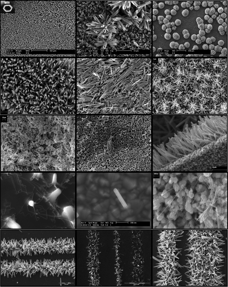
Purpose-built crystalline ZnO structures grown directly onto various substrates (TCO, Si wafers, glass, polypropylene) by controlled aqueous growth at 90 °C.
3.2 SnO2
Another very important post-transition large bandgap semiconductor is tin dioxide, SnO2. It crystallizes in the tetragonal crystal system (space group P42/mnm) and is isostructural with rutile. The unit cell consists of two tin atoms and four oxygen atoms. The octahedra are sharing edges and form linear chains along the c-axis. Consequently, the highest electron density is observed along the c-axis as well as high polarizability and birefringence. The low index (110) face has no net dipole moment in the [110] direction and is therefore a nonpolar surface and represents the thermodynamically most stable bulk termination [31] and lowest surface energy [32]. In such stoichiometric surface, in which one-half of the surface cations are fivefold coordinated with O ions and the other half are sixfold coordinated because of the presence of a row of bridging oxygens, yields tin atoms with the formal +IV oxidation state and thus, surface and bulk have similar resistivity. The typical lattice parameters are a = 4.737 Å, and c = 3.186 Å yielding an axial ratio of a:c = 1:0.672. Such centrosymmetric structure of low axial ratio reduces substantially the crystal ability to grow along the [001] direction. For such reason, SnO2 nanorods and nanowires predominantly grow along other crystal directions [33]. Yet, by careful consideration of symmetry and surface stability arguments, highly oriented bundles of c-elongated SnO2 nanorods (aspect ratio of 1:10) with square cross section and (110) side faces can be generated [20] along with other anisotropic and porous nanostructures as shown on Fig. 3.
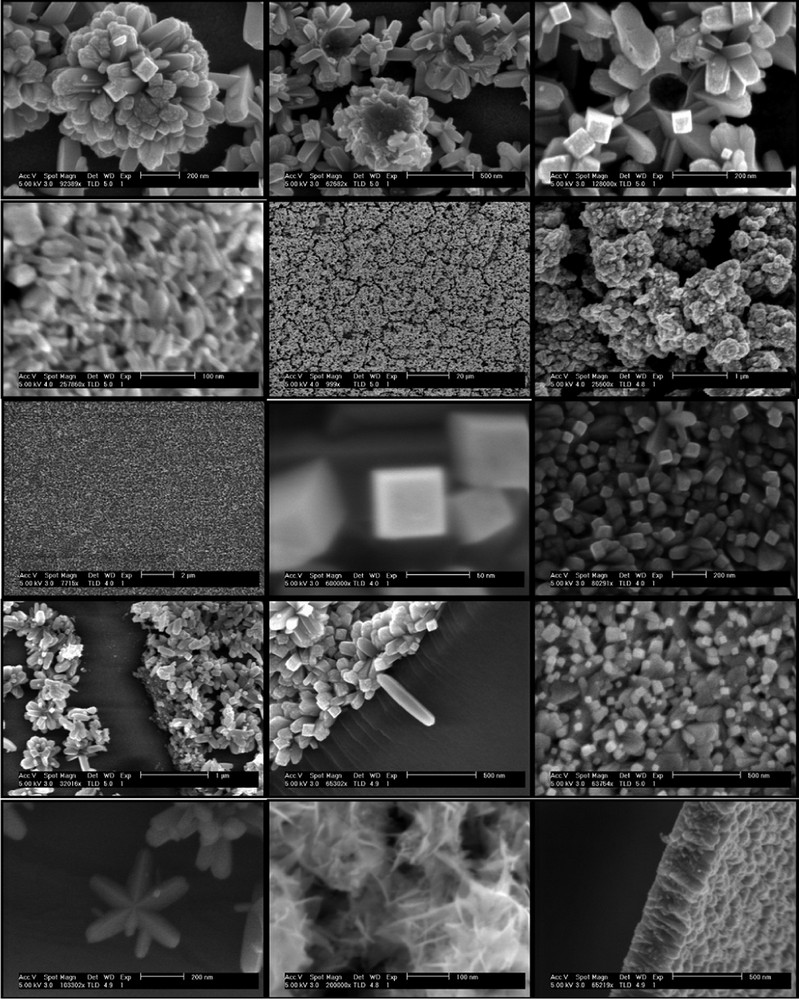
Purpose-built crystalline SnO2 nanostructures grown directly onto various substrates (TCO, Si wafers, glass) by controlled aqueous growth at 95 °C.
3.3 α-Fe2O3
Due to its structural and thermal stability, its resistance to photocorrosion, its high quantum efficiency as well as its low cost of fabrication and availability, α-Fe2O3 (hematite) the thermodynamic stable phase of iron(III) oxides is another candidate of choice for photoelectrochemical devices [34]. Fig. 4 illustrates the ability of the aqueous chemical growth technique to design advanced purpose-built nanomaterials. The SEM pictures show 3-D arrays of metal oxides consisting of aligned nanorods with various controlled orientations onto the substrates. The α-Fe2O3 arrays consist of 50 nm nanorod bundles, made of nanowires of 3–4 nm in diameter and about 0.7–1 μm in length regardless of their orientation. Such advanced particulate thin films have been designed to develop electrodes for wet photovoltaic cells. Indeed, the diameter of the nanowires (within the bundles) is an excellent match of the minority carrier diffusion length of hematite. Thus, the photogenerated holes have a very short distance to reach the interface and so, they do not recombine easily with photogenerated electrons. Accordingly, a very efficient charge separation occurred along with a high incident photon-to-electron conversion efficiency (IPCE), which led to the creation of a 2-electrode hematite photovoltaic cells [12] and photocatalytic cells for the photo-oxidation of water [13]. In addition to applied knowledge and device optimization, a general fundamental understanding has been developed by probing and demonstrating the influence of the orientation of nanoparticles on the photoelectrochemical properties of metal oxide photoanodes. Besides the designed grain boundary-free direct electron pathway and the structural match for the hole diffusion length, a quantum confinement has also been suggested which is currently being investigated by resonant inelastic X-ray scattering (RIXS) at synchrotron radiation source facility [35].
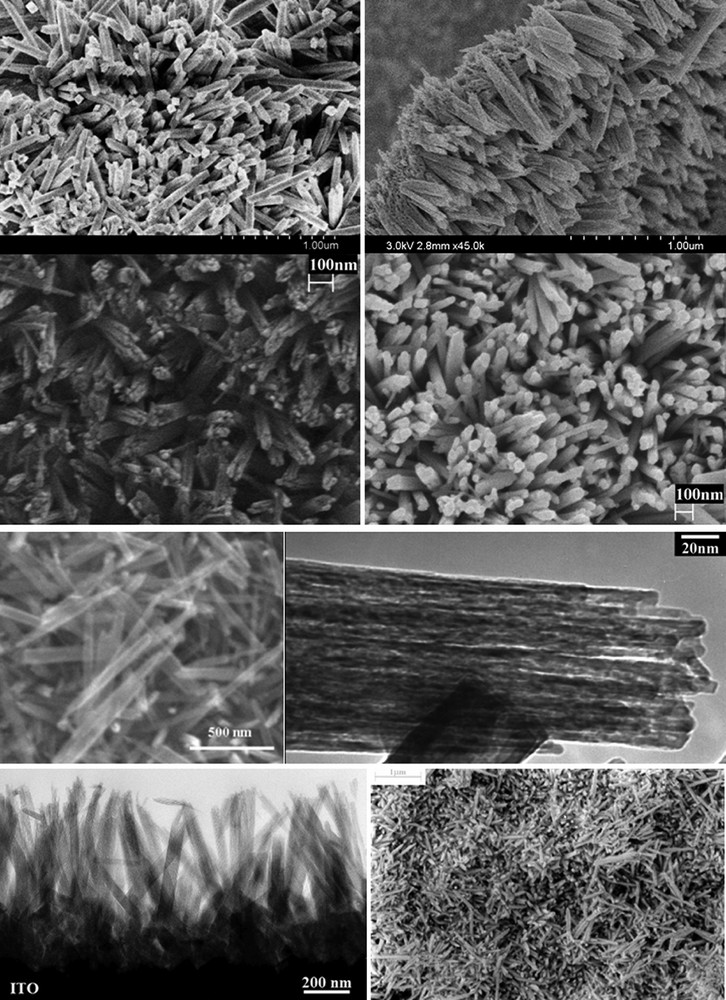
SEM images of purpose-built crystalline α-Fe2O3 grown directly onto various substrates (TCO, Si wafers, sapphire) by controlled aqueous growth at 95 °C.
4 Conclusion and perspectives
Transition and post-transition metal oxide semiconductor materials with optimized and nanoengineered oriented morphology and architecture have been fabricated directly onto various substrates at low cost and at large scale from an aqueous growth technique. Photocatalysis and photovoltaics should benefit from these materials and promising improvements in terms of sensitivity, selectivity, and overall efficiency could be demonstrated with the use of such designed, functional and innovative nanostructures.