

1 Introduction
Since the first electrochemical porosification carried out onto silicon by Uhlir [1], an increasing interest in porous semiconductors has arisen. The research on these small-dimension structures is closely associated with shrinkage of electronic devices. Besides, a lot of original properties and applications of porous silicon have been reported (e.g., optics and biology [2]). Numerous studies on porosification process and pore morphologies have thus been performed on III–V semiconductors (see, e.g., Refs. [3–5]). The influence of the solvent, the conducting salts [6–8], the current density and the applied potential [2] have been studied. These investigations have mainly been achieved on Si, while fewer studies have been performed on III–V semiconductors. In water, the pore formation models were initially built up for Si (see, e.g., Refs. [9–11]), and have been extended to III–V semiconductors (see, e.g., Refs. [12–14]). Two approaches are mainly proposed in literature: “chemical” and “physical” models. The selection of an appropriate solvent, pH and conducting salt remains, however, a crucial parameter for the resulting pore morphology [15].
Liquid ammonia exhibits a physico-chemistry very different from that of other common solvents (see, e.g., Ref. [16]). Its dielectric constant and viscosity are four times lower than those of water. Thus, many compounds such as alkaline metals or solvated electron can be solvated in this original medium. In contrast to other non-aqueous solvents, electronic-grade NH3 provides true water-free conditions. Thus, liquid ammonia is an interesting candidate to study the influence of the surface chemistry on semiconductors without oxide formation.
In a previous work, porous etching onto n-GaAs and n-InP, in this medium, has been reported [17,18]. In the present paper, the anodic behavior of n-InP in acidic liquid ammonia will be described. The electrochemical response was studied in potentiodynamic and galvanostatic modes. Afterward, the morphology of the as-grown layers was examined by scanning electron microscopy (SEM). Finally, photoluminescence (PL) characterizations were carried out in order to determine the optical and electronic properties of the porous layer.
2 Experimental
Sn-doped n-InP (100) wafers (ND = 1018 at cm−3) were purchased from INPact Inc. and cleaved in 10 mm2 rectangles. Prior to use, samples were chemo-mechanically polished with Br2–methanol, soaked in 2 M H2SO4 to remove any native oxides and finally rinsed with ultra-pure water. The ammonia condensation process has already been described in a previous work [18]. The working temperature was 223 K. Anhydrous 1 M NH4Br (highly soluble in NH3 liq.: 2.38 g per g of NH3 [16]) has been used as a conducting salt and leads to a strongly acidified solution: pH = 0 in liquid ammonia's pH scale.
The electrochemical setup was a classical three-electrode cell. Pt and Ag wires served, respectively, as counter and reference electrodes. In this article, all potentials refer to the silver reference electrode (ESRE° = 0.79 V/SHE [19]). Galvanostatic treatments were performed in the dark with a PAR EG&G 273 potentiostat–galvanostat. The surface modifications were examined using a scanning electron microscope in top view and cross-section using a JEOL JSM 5800LV. The optical properties have been analyzed by ex situ photoluminescence measurements at room temperature using a He–Ne laser (λ = 633 nm) as excitation source. Luminescence at the front was a collected using and optical setup of lenses, a Jobin Yvon HR320 monochromator and a 3378 Pacific Instrument photomultiplier.
3 Results
3.1 Electrochemical behavior
Fig. 1a shows the evolution of the current density against the applied potential (J–E), varying from −0.1 to 1.7 V at 20 mV/s. A reproducible anodic peak appears at 1.3 V on the forward scan and is followed by an apparently unlimited current at E = 1.7 V. This anodic wave is neither detected on the return sweep nor on the following sweeps. This phenomenon corresponds to a passivation of the surface. The formation of a thin passivating film has indeed been recently reported [20,21]. The layer is an insoluble compound in which no indium has been detected by X-ray photoelectron spectroscopy. A chemical composition close to “HNP–NH2” (phosphinimidic amide-like) has been suggested, with an estimated thickness lower than 10 nm.
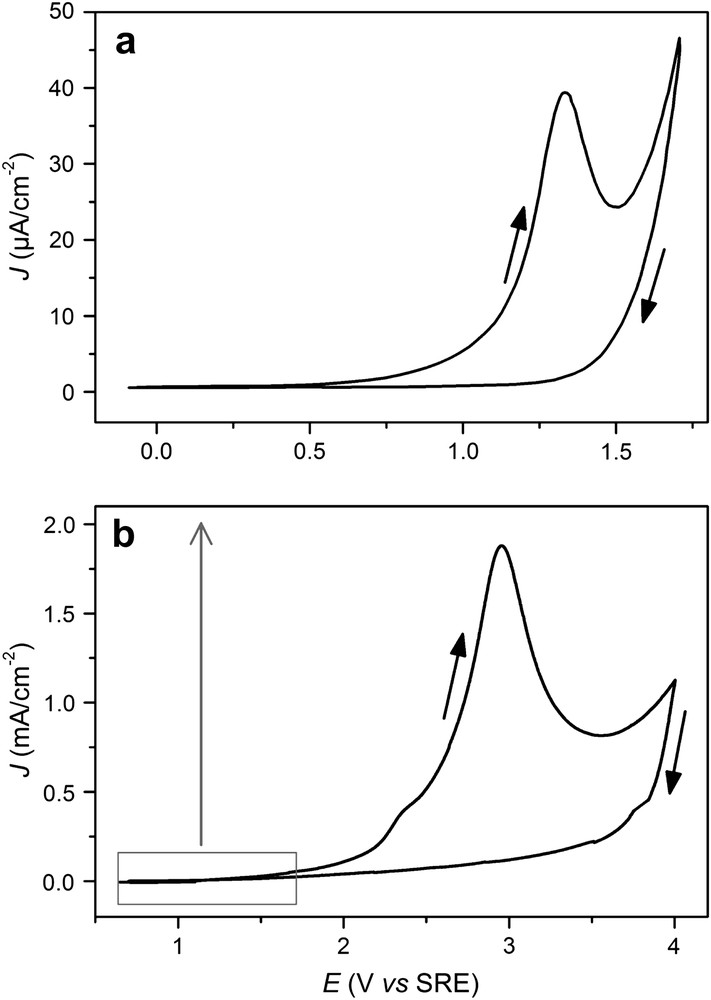
Current density vs. potential curves for n-InP in acidic liquid ammonia (1 M NH4Br) at 223 K in the dark. The potential was scanned at 20 mV/s from (a) −0.1 to 1.7 V and from (b) 0.6 to 4 V.
Fig. 1b presents a potentiodynamic curve performed in a wider range of potential from 0.6 to 4 V at 20 mV/s. In this case, on the forward scan, an anodic peak is observed at 3 V (J ≈ 1.8 mA cm−2), while a flat current is measured on the reverse scan. This anodic peak corresponds to a strongly higher coulometric charge (ca. 70 mC cm−2) than the anodic peak shown in Fig. 1a (ca. 1 mC cm−2). The small shoulder at 2.3 V indicates that the steep current increase observed at 1.7 V in Fig. 1a was not an unlimited evolution. In a previous work [17], chemical analyses have revealed the dissolution of semiconductor for potential higher than 1.7 V. After 3 V, the current density decrease can be attributed to the simultaneous substrate dissolution and corrosion product precipitation on the surface. Note that in the whole voltage range, NH3 oxidation occurs simultaneously.
Galvanostatic treatments have been performed in different current ranges. For very low applied current densities (J < 0.1 mA cm−2), the potential reaches progressively the voltage range corresponding to the apparently unlimited current, from 1.5 to 2 V (see Fig. 1a). Due to the very low anodic charge involved, no surface modifications were detected by SEM.
Figs. 2 and 3 present E–Q curves corresponding to two higher applied current ranges: low (0.1 < J < 1 mA cm−2) and high currents (J > 1 mA cm−2). For the three low current densities (Fig. 2a–c), a very similar evolution of the potential is measured: a steep increase from ocp to approximately 2 V followed by a plateau. Note an unexplained potential perturbation centered at Q = 1 C cm−2. For anodic charges lower than 1 mC cm−2, only slight dissolution of the surface was noticed.
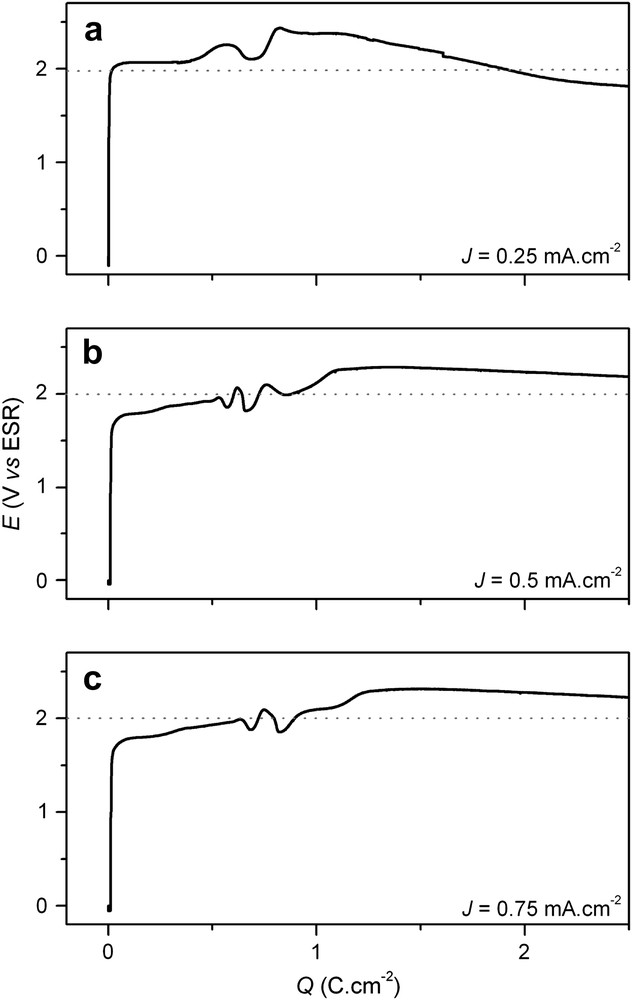
Electrode potential-time curves for n-InP in acidic liquid ammonia (1 M NH4Br) at 223 K. The electrodes were anodized at constant currents: (a) 0.25 mA cm−2, (b) 0.5 mA cm−2 and (c) 0.75 mA cm−2.
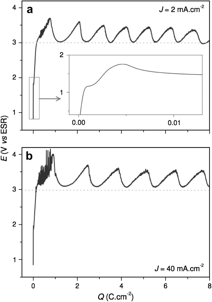
Electrode potential-time curves for n-InP in acidic liquid ammonia (1 M NH4Br) at 223 K. The electrodes were anodized at constant currents: (a) 2 mA cm−2 and (b) 40 mA cm−2.
As seen in Fig. 3, whatever the high applied current density (J > 1 mA cm−2) the general variation of the potential with Q is roughly identical. In contrast to low currents (Fig. 2), potential increases steeply from ocp to approximately 3.5 V and oscillates regularly around ca. 3.25 V, with an average amplitude of 0.5 V. This potential range corresponds to the descending side of the anodic peak shown in Fig. 1b. In a previous work, it has been shown that the oscillation frequency depends linearly on the current (f varies from 1 to 100 mHz) [18]. Additionally micro-oscillations (Hz range) are measured and could be ascribed to the evacuation of dissolved materials out of pores that correspond to thin and deep diffusion channels. As presented in previous works [18,20], the evolution of E with Q can be divided in three steps: nucleation, pore growth and formation of multilayered structure. The first step (Q < 150 mC cm−2) is presented in inset in Fig. 3a. It is associated with the formation of the phosphinimidic passive layer (Q ≈ 1 mC cm−2), followed by an increase of E until 2.8 V (5 < Q < 150 mC cm−2) corresponding of the nucleation of the pores. It is noteworthy that micro-oscillations are not visible in the enlarged view, since the evacuation does not proceed yet through deep pores. The second step (0.15 < Q < 1.2 C cm−2) corresponds to the first potential oscillation that is related to pore growth. During this initial channel elongation, a strong perturbed potential is observed, especially for the highest current density. In the third domain (Q > 1.2 C cm−2), the macro-oscillations (mHz) regime goes on. The oscillation amplitude is gradually faded out. It has already been attributed to the formation of a multilayered porous structure [18].
3.2 Surface modification
In the case of low applied current densities (0.1 mA cm−2 < J < 1 mA cm−2), a thick film is formed on the surface. Figs. 4 and 5 present both cross-sectional and top views of InP surfaces after anodic treatments performed at 0.25 and 0.75 mA cm−2, respectively. In both cases, a rough, spongiform and cracked film are formed (Figs. 4b and 5b). According to the SEM cross-sections (Figs. 4a and 5a), the films are definitely not compact, but their spongy aspect cannot be associated with a porous etching since no tubular features are grown in the bulk material. These films exhibit a thickness in the micrometer range. The chemical nature of this layer is not yet determined. It could correspond to dissolution–precipitation of corrosion products. A preliminary study by X-ray diffraction has demonstrated the amorphous nature of this layer. The surface underneath is etched and shows a non-uniform dissolution front: small hemispherical depressions are observed (Figs. 4a and 5a). Note that pores can appear locally for J close to 1 mA cm−2. These pores present a sponge-like structure without specific orientation: no channels are detected.

SEM images of n-InP electrodes after galvanostatic treatment in acidic liquid ammonia (1 M NH4Br) at 223 K. The electrode was anodized at a constant current of 0.25 mA cm−2 for 5 C cm−2 (a) cross-section and (b) top view.
SEM images of n-InP electrodes after galvanostatic treatment in acidic liquid ammonia (1 M NH4Br) at 223 K. The electrode was anodized at a constant current of 0.75 mA cm−2 for 10 C cm−2; (a) cross-section and (b) top view.
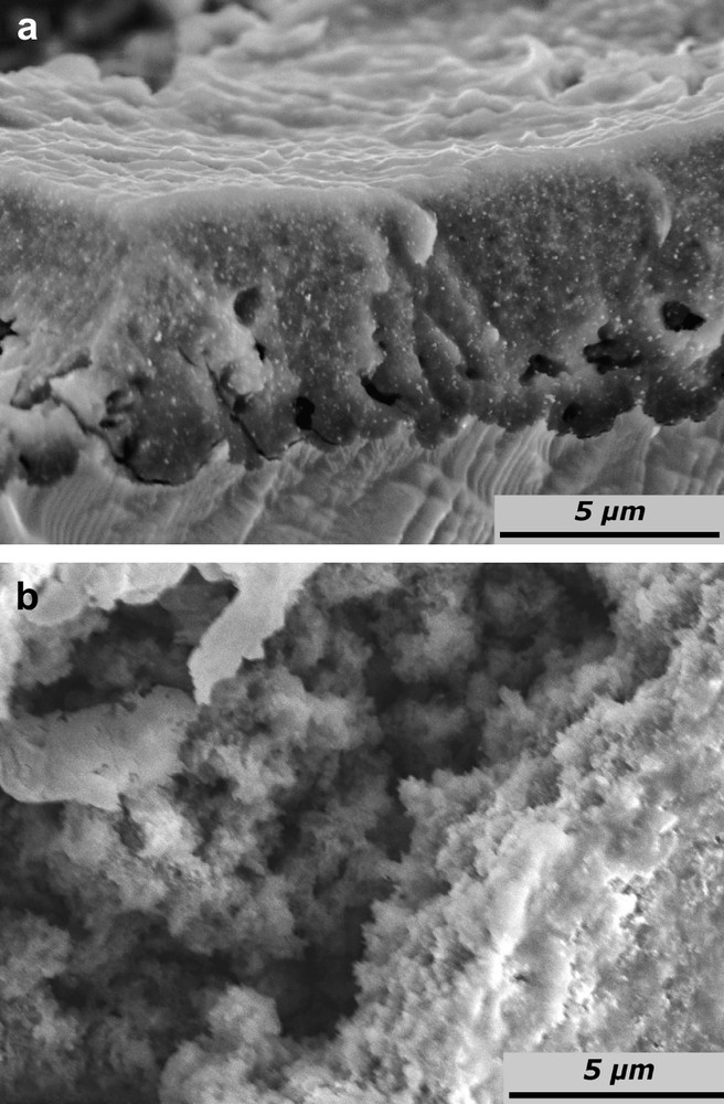
Another morphology is observed when high current densities are applied (1 mA cm−2 < J < 100 mA cm−2). SEM images for a sample anodized with J = 40 mA cm−2 are reported in Fig. 6. Note that pictures corresponding to J = 2 mA cm−2 exhibit a very similar morphology and have been presented in a previous work [18,20]. Pores are tortuous current line oriented (t-CLO) and are grown in hemispherical depressions (Fig. 6a). The thickness of the pore walls is 60 nm and the diameter of pores is of 140 nm (Fig. 6b). In contrast to aqueous media, no diameter oscillations are observed. The layer presents a maximum thickness of 3 μm; this corresponds to a synchronized lift-off of the porous layer and is correlated to macro-oscillations of E. This material detachment leads to the loss of the initial flatness of the surface. Since these detached layers remain on the surface, they pile up themselves: a multilayered structure is obtained [20].
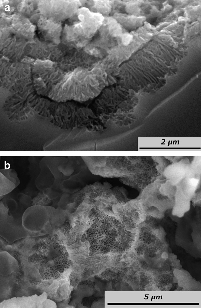
SEM images of n-InP electrodes after galvanostatic treatment in acidic liquid ammonia (1 M NH4Br) at 223 K. The electrode was anodized at a constant current of 40 mA cm−2 for 12 C cm−2; (a) cross-section and (b) top view.
3.3 Photoluminescence analysis
The optical properties of the anodized samples were investigated by PL measurements. Fig. 7 shows the relative photoluminescence intensity (IPL) against the wavelength (λ = 780–1020 nm) for a reference sample and InP surfaces porosified using three different current densities with a constant coulometric charge of 400 mC cm−2. In all cases, the photoluminescence spectrum is very stable in time. The IPL maximum is observed at λ = 920 nm. This value corresponds to the band-to-band transition (Eg = 1.35 eV). The anodic treatments do not modify either the position of the peak or the full-width at half maximum (FWHM). Thus, no shift occurs and no additional PL contribution appears for all currents. Nevertheless an IPL drop is measured for the porous samples. This decay is approximately 20% for J = 0.5 mA cm−2, whereas for the higher applied currents (J = 2–50 mA cm−2) it is roughly 30%.
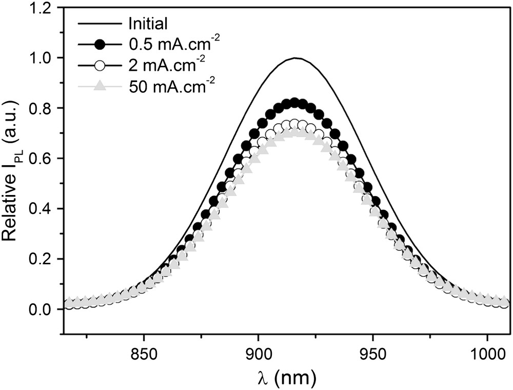
Normalized photoluminescence responses of n-InP electrodes after galvanostatic treatments in acidic liquid ammonia (1 M NH4Br) at 223 K. The electrodes were anodized at constant currents for 0.4 C cm−2.
4 Discussion
Pore formation in liquid ammonia appears to be different in numerous aspects as compared to the porous etching carried out in aqueous medium. Depending on the applied current, different phenomena occur on the InP surface: a thick film is formed for low current (0.1 mA cm−2 < J < 1 mA cm−2) while porous etching takes place for higher currents. Conversely, in aqueous solutions, there is a competition between porous etching and electropolishing, but no compact films are observed (i.e. electrolytes used for InP dissolution do not lead to stable oxide layers). In contrast to water, crystallographic oriented pores have not been observed yet in NH3 liq. In aqueous solutions, a wide variety of pore morphologies have been reported: depending on the applied polarization, crystal or current-line-oriented pores are formed [15]. In this solvent the thickness of the porous structures is not limited, whereas a constant pore depth (ca. 3 μm) is obtained in liquid ammonia. Deeper structures correspond to the piling up of such 3 μm thick porous layers and are related to the potential macro-oscillations (mHz range) observed at high current densities. In contrast, in water, voltage oscillations are associated with periodic pore diameter variation and can be explained using the current burst model [11]. As seen on the SEM cross-sections (Figs. 4–6), the initial flatness of the surface is progressively lost, the etching front is very perturbed and it is composed by hemispherical depressions. This morphological feature is not observed in water media. It could reveal a heterogeneous spreading of the current in the material due to a non-uniform electric field distribution. When the hemispherical structures are formed, similarly to water, pores elongate perpendicularly to the initial surface, i.e. along the current lines (see Fig. 6b). Finally, the main difference between porous etching in water and liquid ammonia is related to the initial passivation layer. In NH3 liq., a thin phosphinimidic amide-like layer is grown. This film exhibits passivating properties and is chemically very stable [21]. In water, the “chemical” models are based on the anodic formation of an oxide and its subsequent chemical dissolution, while in the “physical” approaches, no oxide growth is considered and local dissolution is attributed to the space charge layer present at the semiconductor surface. In both cases, these models do not fulfill the description of the pore formation in liquid ammonia.
In the literature, PL characterizations of porous n-InP have revealed strongly different results. Blue shift [22], red shift [23], IPL quenching [24,18,25] as well as formation of additional peak [24,26] have been reported. PL blue shift is usually due to the quantum-size effect, while red shift reveals a sub-band gap emission that can be attributed to the creation of surface states (e.g. impurity absorption or corrosion products). IPL quenching is attributed to the so-called “dead” layer phenomenon and formation of supplementary PL peaks are ascribed to the enhancement of an oxide response (λ = 450 nm) due to the very high specific area of the porous surface. Note that this last effect cannot be studied in the present case since the excitation source has a higher wavelength (λ = 633 nm).
After the anodic treatments carried out onto n-InP in liquid ammonia, PL measurements do not exhibit any shifts and show exclusively an intensity decrease. The blue shift is indeed not expected since the pore walls exhibit dimensions clearly higher than the Bohr radius of the exciton (rB = 19 nm for InP). Additionally, no radiative centers seem to be created during the porous etching, as no photoluminescence red shift is detected.
The IPL decrease can, however, be explained by the formation of an absorbent film. Depending on the applied current range, the absorbent properties of the film do not have the same origin. At low currents (0.1 mA cm−2 < J < 1 mA cm−2), one can assume that the thick layer described in Section 3.2 behaves like an absorbent film. Therefore, the IPL quenching should depend on the thickness of the film. Note that the phosphinimidic amide-like film does not modify the PL spectrum of an intact InP sample. At high currents (J > 1 mA cm−2), the pore geometry is, however, compatible with a decrease of the PL intensity according to the “dead” layer model [27]. After etching, the pore wall thickness is indeed in the range of width of the space charge layer of the semiconductor. This leads to establish majority carrier depletion and a separating electric field in the whole porous region. Photoexcited holes generated in this zone will experience an electric driving force towards the surface where non-radiative processes are also likely to dominate. The photoluminescence of bulk InP is thus progressively masked when the porous layer, which acts as a “dead” layer, grows.
5 Conclusion
Anodic treatments performed onto n-InP in acidic liquid ammonia have provided different surface modifications. At low current densities, a thick amorphous film is formed on the surface. Its chemical composition is not yet determined. In this regime, porous structures are sometimes present at the interface between this film and bulk InP. In contrast, for high current densities, an original multilayered t-CLO porous morphology is obtained. The presence of an insoluble passive layer on surface prior to formation of both thick amorphous film and t-CLO pores suggests that new models should be developed to describe the porous etching mechanisms in liquid ammonia. At both low and high applied currents, the films exhibit absorbent properties since the PL signal is not shifted but quenched. The absorption of t-CLO films is ascribed to the “dead” layer behavior of the porous layer.
Vous devez vous connecter pour continuer.
S'authentifier