

1 Introduction
In aqueous media, electrochemical methods can be used to control the growth of various kinds of oxide structures onto InP surfaces [1–9]. Previous works have established that the local oxidation conditions are crucial; a “constrained” or “non-constrained” process will give rise to a final homogeneous or heterogeneous interfacial layer with a specific chemical composition that will determine the resulting electrical properties [10,13]. In particular, at pH = 9, depending on the anodization parameters, very different anodic layers are grown, whose composition, thickness and electrical properties strongly rely on the applied current density [13,14]: low current density leads to a thin InPO4-like layer exhibiting good electrical properties. Conversely, when the oxidation is performed with high current densities, thicker In-rich oxide films without chemical and electrical blocking properties are produced. These previous works demonstrate a correlation between composition, texture and electrical properties.
In the present paper, a galvanostatic method has been used to prepare anodic films, with current densities ranging from 0.2 to 30 mA cm−2 and durations varying from 2 s to a few minutes. The chemical composition and morphology of the anodic layers have thus been investigated by X-ray photoelectron spectroscopy (XPS) and atomic force microscopy (AFM), respectively, and have been correlated to the passivating properties of InP/oxide interfaces characterized by capacitance–voltage measurements.
2 Experimental
Anodic oxidation was performed onto n-InP (100) wafers from INPact Inc. (Sn doped, ND = 1018 at cm−3). The electrodes were cleaved in 0.1-cm2 pieces and chemo-mechanically polished with a Br2–methanol solution and successively rinsed with pure methanol and water. In order to remove residual oxides, samples were dipped during a few minutes in 2 M HCl, prior to the experiments. Electrochemical experiments were performed in a borate buffered Tritisol (Merck) solution, at pH = 9, using a classical three-electrode configuration with a Mercury Sulfate Electrode (EMSE = +0.65 V/SHE) as a reference and a Pt wire as a counter electrode. The electrochemical cell was connected to a PAR 283 potentiostat/galvanostat and placed in the dark. Oxidation treatments have been performed by applying a constant anodic current density, ja, ranging from 0.2 to 30 mA cm−2 for durations varying from 2 s till a few minutes.
Capacitance vs. potential (C–V) measurements have been used to investigate the oxide passivating properties. C(V) measurements were carried out before and after oxidation treatments using a PAR 283 potentiostat and an EG&G 5210 lock-in amplifier. The perturbating AC-voltage frequency is set to 1107 Hz with an amplitude of 20 mV and the DC-voltage scan rate was 10 mV/s.
XPS analysis was performed using a VG-Escalab 220 iXL spectrometer. A focused monochromated X-ray beam (Al Kα) was used as excitation source while detection was performed using a constant analyzer energy with a threshold energy of 8 or 20 eV; photoelectrons were collected perpendicularly to the surface.
Atomic force microscopy was used to characterize the topography of oxide films. A Dimension 3100 microscope (Veeco Instruments) equipped with a pyramidal Si3N4 tip was used in contact mode. Forces in the range of 100 nN were applied to image the surface. Both root mean square (Rrms) and averaged (Ra) roughness were calculated using the manufacturer software.
3 Results
3.1 Anodic oxide growth
Oxide growth has been achieved by galvanostatic polarizations using current densities in two different ranges. The first surface modification consisted in applying a low current density: 0.2 mA cm−2 for 300 s, while a stronger perturbation was applied to the InP/electrolyte interface during the second treatment: 30 mA cm−2 for 2 s. In both treatments, named “non-constrained” and “constrained”, respectively, the durations have been adjusted in order to apply a similar anodic coulometric charge (Qa = 60 mC cm−2) to the samples.
The evolutions of the potential against the oxidation time (U–t) for low and high currents are, respectively, given in Fig. 1a and b. When ja = 0.2 mA cm−2, the potential reaches instantaneously an average value close to 1.5 V and stabilizes after 20 s at nearly 1.6 V after a small decrease. The potential evolution is strongly different when the higher current density (ja = 30 mA cm−2) is applied. It reaches directly 4 V and remains increasing up to 8–9 V after 0.25 s of treatment. These different U–t curves indicate that the oxide growth proceeds differently according to the applied current density. The resulting in situ capacitance–voltage measurements and ex situ XPS and AFM characterizations have been compared for the two oxidized surfaces.
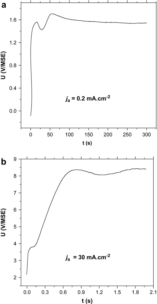
Potential-time evolution during anodic treatment in borate buffer (pH = 9) at ja = 0.2 mA cm−2 (a) and ja = 30 mA cm−2 (b).
3.2 Electrical characterization: capacitance–voltage measurements
By coupling XPS and photocurrent analysis, previous works have shown that capacitance–voltage measurements performed, before and after the semiconductor surface oxidation, are very sensitive to oxide coverage and passivating properties [10–15]. Compared to the initial C−2–V response (Mott–Schottky representation, MS), a flat plot (constant C−2 values) has been measured for a semiconductor surface covered with a thin oxide film with good passivating properties. On the other hand, linear Mott–Schottky behaviors with a similar or decreased slope, compared to the bare InP surface, have been attributed to inhomogeneous oxide layers exhibiting poor electrical properties, either oxide islands (the MS slope remains constant) or thick and probably porous oxidized films (the MS slope decreases).
In the present work, capacitance–voltage curves obtained before and after the anodic treatments are given in Fig. 2a and b. The C–V measurements performed on bare samples are very reproducible and give an apparent donor density close to the value indicated by the wafer provider (with ɛInP = 9.3, ND ≈ 1018 cm−3). As expected at pH = 9, the extrapolated flat band potential is approximately equal to −1.2 V/MSE. Very different MS responses are, however, obtained after the two anodic oxide growths.
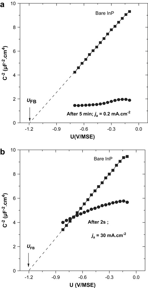
Mott–Schottky plots on n-InP performed in borate buffer (pH = 9) with a perturbation frequency of 1107 Hz. (a) Before and after anodic oxidation at ja = 0.2 mA cm−2 for 300 s and (b) before and after anodic oxidation in borate buffer at ja = 30 mA cm−2 for 2 s.
When the oxidation is performed using the low current density, a nearly flat C−2–V curve is observed. In these conditions, the global capacitance is high (C ≈ 1 μF cm−2) and constant over a potential range of 1 V. This constant capacitance suggests that the applied potential entirely drops in a homogeneous oxidized layer, keeping a constant band bending at the semiconductor/oxide interface. A similar result is described in Ref. [13]. The global capacitance resulting from this semiconductor/oxide/electrolyte interface is then given by the following equation:
| (1) |
For the second treatment, performed with a higher current density, while the coulometric charge is unchanged, the Mott–Schottky response is strongly different. A linear variation of the global capacitance with the applied potential is measured. This C–V evolution suggests the presence of an oxide layer presenting poor electrical properties. In a previous work, this behavior was attributed to the presence of a heterogeneous coverage of the semiconductor surface.
3.3 Chemical analysis: X-ray photoelectron spectroscopy
The chemical composition of both oxide types has been studied by XPS. Fig. 3 presents the evolution of and P2p photoelectron peaks before (Fig. 3a) and after (Fig. 3b) oxidation at low current density. After the anodic treatment, additional contributions positively shifted in binding energy appear on the spectra (see Fig. 3b). It evidences therefore the presence of oxidized phases in which In and P atoms are bounded to O atoms. A quantitative analysis of these spectra has been carried out in a previous work [13]. For each fitting treatment, the P2p and In3d levels were kept associated by constraints on InP bulk response: fixed fwhm for InInP and PInP contributions and corrected ratio In(InP)/P(InP) = 1 ± 0.1. It appears that P2p can be perfectly fitted with two contributions: one associated with the bulk, PInP, and the other one with oxide, Pox. For or 5/2, when the InP bulk component, InInP, is fixed, one or two additional components must be added to describe the oxide phase's contribution, Inox. Table 1 gives the values of area ratios of both phosphorus and indium contributions: Pox/PInP, Inox/InInP, for oxidation times equal to 30 and 300 s. These analyses evidenced the growth of thin oxide layers of thickness limited to 3–5 nm, with a composition close to that of InPO4.
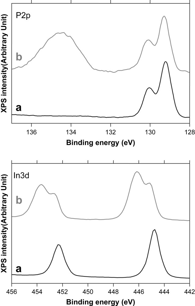
XPS spectra carried out onto n-InP (a) clean surface, (b) after anodic oxidation in borate buffer at ja = 0.2 mA cm−2 for tox ≥ 30 s.
Values of area ratios of both phosphorus and indium contributions: Pox/PInP, Inox/InInP, for oxidation times of 30 and 300 s
| tox (s) | Pox/PInP | Inox/InInP | dox (Å) |
| 30 | 1.28 | 1.8–2.55 | 18–29 |
| 300 | 2 | 3 | 25–40 |
When anodic treatments are performed using a high current density (ja = 10–50 mA cm−2), XPS results are strongly different [13,14]. and P2p spectra obtained on different films evidence the presence of oxidized phases in which In and P atoms are present. Inversely, for analyses performed after the “non-constrained” treatment, the XPS signal corresponding to the InP substrate is almost masked, revealing the presence of thick (a few 10 nm) and indium-enriched oxide layers. It is noteworthy that XPS analyses were not very reproducible for this oxidation mode. It is – maybe – related to a heterogeneous and chaotic film.
3.4 Morphological observation: atomic force microscopy
Atomic force microscopy has been used to investigate the morphology of the layers grown in both “constrained” and “non-constrained” modes. Fig. 4 presents the 3D views of InP surfaces before and after the two anodic oxidations, while Table 2 reports the evolution of root mean square (Rrms) and averaged (Ra) roughness corresponding to the different surfaces.
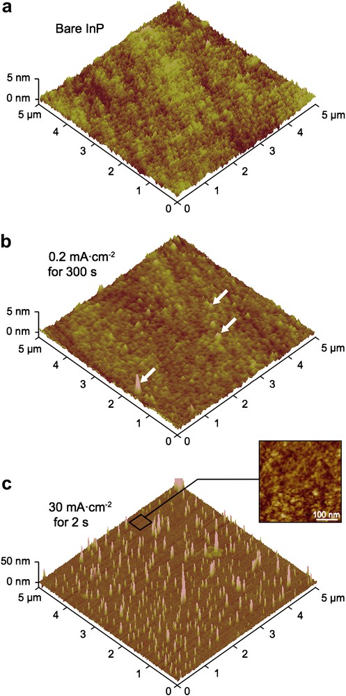
AFM 3D view of n-InP surface after (a) chemo-mechanical polishing with Br2–methanol, (b) anodic oxidation in borate buffer at 0.2 mA cm−2 for 5 min, (c) after anodic oxidation in borate buffer at 30 mA cm−2 for 2 s. White arrows in (b) point out an example of the globular features reported in the text. Inset in (c) presents an enlarged top view of the surface (z-scale = 5 nm).
Evolution of root mean square (Rrms) and averaged (Ra) roughness corresponding to the different surfaces
| Initial | Oxidized (300 s, 0.2 mA cm−2) | Oxidized (2 s, 30 mA cm−2) | |
| Rrms (nm) | 0.20 | 0.26 | 5.10 |
| Ra (nm) | 0.15 | 0.19 | 1.80 |
The initial InP surface (Fig. 4a), obtained after a chemo-mechanical polishing with Br2–methanol, exhibits a flat and smooth morphology: Rrms and Ra values are close to 0.2 and 0.15 nm, respectively. Fig. 4b shows the surface topography after low-current oxidation. A flat and relatively homogeneous surface is observed. The roughness increases slightly: Rrms = 0.26 nm and Ra = 0.19 nm. Some globular features exhibiting a mean diameter, a maximum height and a density of approximately 50, 3 nm and 2 × 108 cm−2, respectively, are, however, observed (see white arrows on the figure). A heterogeneous and strongly different surface morphology is observed after the high-current treatment (Fig. 4c). Relatively thick islands exhibiting a height in the 20-nm range and a mean diameter of approximately 50 nm cover the InP surface. In this case, the particle density is much higher than after the low-current treatment: 14 × 108 islands per cm2. Obviously, the global roughness is maximum (Rrms = 5.1 nm and Ra = 1.8 nm), but the surface roughness when the islands are not taken into account is also higher than that of the bare and non-constrained oxidized InP surfaces: Rrms = 0.76 nm, Ra = 0.60 nm (see the enlarged top view presented in Fig. 4c). Similar observations have been performed for the anodic oxidation of n-InSb in NaOH [15]. Although a compact and dense oxide film was grown at low applied current, a stressed, rough and porous film covered by hemispherical features was formed when high current was used. Such oxide morphology was correlated to poor electrical properties of the layer, i.e. a low-voltage breakdown.
4 Discussion
Although a similar coulometric charge (Qa = 60 mC cm−2) is involved in both anodic treatments, capacitance–voltage measurements, XPS analyses and AFM examinations evidence the formation of strongly different oxidized phases. It indicates therefore that electrical, chemical and morphological properties are correlated. C−2–V plots point out better passivating properties for the “non-constrained” oxide films, and chemical analyses performed on the two types of oxide films reveal also significant differences. Homogeneous and thickness-limited (dox ≤ 3–5 nm) films are grown using a low current while heterogeneous and thick (dox ≈ 10 nm and not limited) layers are formed applying a high current density. Additionally the “constrained” oxide films exhibit a non-reproducible chemical composition. Finally AFM characterization indicates that the low-current oxide exhibits a flat and compact surface, suggesting a 2D growth process, while a heterogeneous (presence of islands) and rougher surface is detected in constrained mode, evidencing therefore a 3D growth mechanism.
The coulometric charge involved in the two processes being identical, the maximum amount of oxidized InP molecules, nInP(ox), can be calculated using Eq. (2), in which it is assumed that all electrical charges are involved in semiconductor oxidation and that 6 or 8 elementary charges are consumed by “equivalent molecule” of InP [16]:
| (2) |
In this work, with an anodic charge of 60 mC cm−2, the maximum amount of oxidized molecules corresponds to roughly 60 ML (i.e. dox ≈ 60 nm). This value is not consistent with XPS measurements since the oxide thickness is in the range of 3–5 and 10–20 nm for low- and high-current conditions, respectively. The faradic efficiency is thus far from unity. In the case of “non-constrained” oxidation, the film thickness is self-limited. It is probably due to its very good passivating properties correlated with its homogeneous chemical composition and its dense and smooth morphology. As soon as the oxide is formed, the applied current seems to be involved in the oxidation of the solvent. On the other hand, the “constrained” process leads to heterogeneous and not self-limited thick films. Although the higher thickness and the presence of spherical grains on the surface, the faradic efficiency is still not full. Oxidation of water can again be suspected but dissolution/precipitation should also be considered, as already suggested on GaAs [17]. The poor electrical properties are again completely correlated with the layer morphology (heterogeneous, rough and probably porous). The bad insulating behavior can be ascribed to the electrolyte interpenetration in the oxide pores, leading to both weaker blocking properties and unlimited film growth. Similarly to oxide layers grown onto n-InSb in NaOH [15], high-current anodization proceeds under a very high electric field (strong band bending, ca. 9 V). It induces both mechanical stress in the film and at the semiconductor/oxide interface and it implies a high defect density in the oxide. Charge transfer can therefore be facilitated by such defects and by the heterogeneous chemical composition of the films.
5 Conclusion
In this work, a successful correlation of morphological investigations with chemical and electrical studies has been presented. It has been established that anodic oxide films grown in borate buffer at pH = 9 by galvanostatic methods (low- and high-current modes) provide very different oxide layers, whose composition, thickness, porosity and electrical properties strongly depend on the applied current density. The 2D growth of a thin homogeneous InPO4-like oxide film has been evidenced when anodic treatment is performed with a low current density, while a thicker porous heterogeneous 3D oxide layer is grown when a higher current is applied. The resulting electrical properties are completely related to the chemical (XPS analysis) and morphological (AFM examination) aspects of the different films: thin and homogeneous films exhibit good passivating behavior, as suggested by the flat and high capacitance value measured on the modified InP/InPO4/electrolyte interface, whereas thick, rough, probably porous and heterogeneous films show poor electrical properties.