

1 Introduction
Multicrystalline silicon is today mainly used to build p–n homojunction solar cells with conversion efficiencies around 15%. Unfortunately, solar electricity is still too expensive [1] and two approaches are investigated to overcome this problem. First, solar cells using smaller quantities of new materials are developed, including heterojunctions between different nanocrystalline semiconductors. The chalcopyrite compound family Cu(In,Ga)(Se,S)2 provides some of the most efficient thin film solar cells [2]. This is mainly due to the high light absorption coefficient of these compounds and a band gap value between 1 and 2.4 eV, which is suitable for photovoltaic application [3]. High efficiencies about 19% have been achieved in laboratory using chalcopyrite based solar cells [2]. The main problem is the use of a toxic selenium gas treatment. Many studies are presently focused on the use of sulfured compounds such as CuInS2. Efficiency of 12.5% [4] has been obtained using CuInS2 thin film based solar cells.
The second approach is focused on the deposition techniques of these materials. The up-scaling of vacuum-based technologies is believed to reduce manufacturing cost effectively. One of the most used vacuum deposition techniques for CuInS2 synthesis is reactive sputtering [5]. Other works focused on ion plating or r.f. sputtering without H2S processing [6–8] to obtain chalcopyrite semiconductors. For example, a two-phase sputtering target, composed of Cu2S and In2S3, has been successfully used [6,7] to prepare CuInS2 thin films. However, in all these cases, chalcopyrite phase is obtained by heating the substrates (400 °C).
An alternative is the use of low-cost thin film deposition techniques. These studies investigated principally chemical bath deposition [9], spray pyrolysis [10] and electrodeposition [11]. However, in precedent electrodeposition and spray pyrolysis techniques, a sulfuration step under H2S gas or sulfur vapour is used in order to control the sulfur concentration in films, or toxic KCN is used to remove secondary copper-rich phase, particularly in spray pyrolysis. In order to avoid such treatment, chemical bath deposition [9] and one-step electrodeposition technique has been successfully used [12–14].
The aim of the present work is to develop direct and safe preparations of nanocrystalline CuInS2 thin layers using one-step electrodeposition and one-step r.f. sputtering [15]. In the context of electrochemistry, sulfur is present in solution as sodium thiosulfate. Moreover, concentration of copper, indium and sulfur precursors was chosen in order to avoid the presence of secondary phases and therefore the use of KCN. For physical vapour deposition, a crystalline chalcopyrite CuInS2 target prepared by solid reaction was used for the first time, making sulfuration treatment unnecessary.
The point of this study is to present the characteristics of CuInS2 thin films obtained by both techniques, especially their optical properties. At this stage, it is important to note that a so-called comparative study of sputtered and electrodeposited CI(S,Se) has been recently published [16]. However, this paper compared CuInS2 thin layers prepared by sputtering with CuInSe2 thin layers synthesised by electrodeposition, considering microstructural and structural aspects. In our work, CuInS2 films were prepared by one-step deposition techniques in order to obtain various structures and microstructures. Furthermore, the objective is to discuss the influence of structure and morphology on the optical absorption of CuInS2 thin films in order to improve solar cells' properties in the future.
2 Experimental details
2.1 Sputtered films
A crystalline CuInS2 target was prepared by mixing Cu2S (Alfa Aesar, 99.5%) and In2S3 (Aldrich, 99.99%) powders. The resulting mixture was calcined at 950 °C for 2 h under vacuum. X-ray Diffraction (XRD) patterns, recorded with a Siemens D5000 Diffractometer using Cu Kα radiation (λ = 0.154 nm), showed that a crystalline CuInS2 chalcopyrite phase was obtained with only 1% Cu2S remaining in the mixture. The resulting powder was then cold pressed in a 4-cm-diameter dye. Energy dispersive X-ray spectroscopy confirmed chalcopyrite composition of the target.
Thin films were prepared by r.f. sputtering at 13.56 MHz frequency using argon plasma in a homemade deposition device. The distance between the target and the substrate was set at 3 cm. ITO glass (Sigma–Aldrich) was used as substrate, cleaned ultrasonically in organic solvents and rinsed in deionised water. The substrate temperature was kept near room temperature. Argon pressure, sputtering power and deposition time were varied as follows: A samples were synthesised using a sputtering power of 50 W under an argon pressure of 2.7 × 10⁻² mbar for different deposition times. B samples were grown with larger sputtering power 70 W under a lower argon pressure, 1.3 × 10⁻² mbar, in order to increase the deposition rate.
2.2 Electrodeposited films
Electrodeposition was carried out potentiostatically in a three-electrode system, using ITO coated glass, platinum grid and standard calomel electrode (SCE) as working electrode, counter electrode and reference electrode, respectively. Cu–In–S layers were prepared using a bath with Cu(OOCCH3)2, InCl3 and Na2S2O3 precursors, with the ratio 10:10:400 mM, respectively. The solution was adjusted with H2SO4 solution to pH = 1.5. The applied potential was −1 V/SCE for 1200 s. Afterwards, films were annealed under vacuum (10−2–10−3 mbar) at 400 °C for 30 min. As-deposited and annealed films will be referred to hereafter as C and D samples, respectively.
2.3 Structural and optical characterizations of films
For both electrodeposition and sputtering, the thickness of the obtained films was determined by a mechanical profilometer DEKTAK 6M. The crystallographic phases were studied by XRD. The surface morphology was observed by SEM using an ESEM PHILIPS 130 and a PHILIPS XL30 scanning field effect gun SEM. The average grain size was monitored by atomic force microscopy (AFM) with a PARK AUTOPROB Cp and calculated from the mean width at half maximum of the (112) X-ray diffraction peak using Scherrer's equation. Transmission spectra were obtained using an AVALIGHT-DHS light source with both deuterium (200–400 nm) and halogen (400–1100 nm) sources. The spectrophotometer is an AVASPEC 2048, with similar wavelength range analysis (200–1100 nm).
3 Results
3.1 Morphology
Sputtered A and B films are very homogenous and adherent, with a brown to grey-blue colour, depending on the thickness. Deposition rates are 2.5 and 6.4 nm/min for A and B samples and thicknesses about 750 and 900 nm are obtained, respectively. Different morphologies for the two sample series are observed. Fig. 1a shows a typical SEM image of sample A: the surface is smooth and composed of grain aggregates. This surface morphology is confirmed by profilometer measurements and by AFM (Fig. 2a). For both A and B series, the average roughness of samples is about 4 nm, which is low in consideration of the 2-nm ITO substrate roughness. Samples are composed of aggregates of crystallites with 50–100 nm size, as determined by AFM, in agreement with about (50 ± 10) nm calculated from XRD.
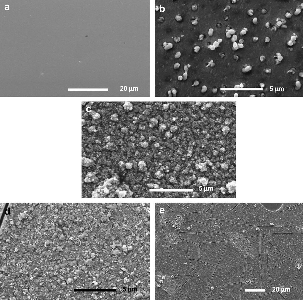
SEM image of (a) A series sputtered films. (b) B series sputtered films. (c) C as-deposited films. (d and e) D electrodeposited annealed films.
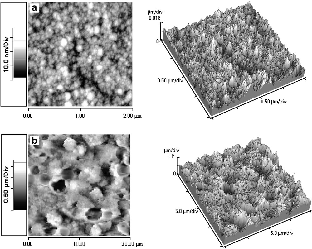
AFM images of (a) A series sputtered films. (b) C series electrodeposited films.
The surface of B samples is covered by small particles of 0.5–1.2 μm diameter, as shown in Fig. 1b. Profilometer measurements are in agreement with the SEM images. These surface particles might be related to two different mechanisms: metallic plot growth [17,18] or projections ejected from the over-heated target if excessive power is applied [19]. However, no entirely consistent mechanism can be proposed at this stage to explain the formation of particles on the films.
Electrodeposited films are very rough with a brown to black colour. Films are adherent after deposition, but are more friable after annealing. Films have about 1.5-μm thickness and the deposition rate was about 75 nm/min. SEM images and profilometer measurements confirmed the high roughness. Dense agglomeration is shown by SEM for sample C as shown in Fig. 1c and in Fig. 1d for sample D. An average grain size of 70–150 nm was determined from AFM observations (Fig. 2b) and about (70 ± 10) nm calculated from XRD. Fig. 1d and e shows SEM images of annealed films D. Numerous cracks are visible on the surface, which could explain the film friability after annealing.
3.2 Structure
Crystalline chalcopyrite films are obtained for large deposition times; for short deposition time the films remain amorphous. The thickness increases until reaching a critical value, at which a part of the amorphous phase crystallizes. This critical thickness was determined for A and B samples at around 300 nm.
X-ray diffractograms of as-deposited sputtered films, both A and B series (Fig. 3), show a strong diffraction peak at 27.8° corresponding to a preferential (112) orientation of crystalline chalcopyrite CuInS2 phase, in good agreement with the literature. This preferential orientation has been noticed in numerous CuInS2 thin films prepared by different techniques [8,16]. This remarkable result was obtained without any substrate heating during deposition [7], post-annealing or chemical treatments with KCN [8]. After annealing at 400 °C, other peaks appear at 46.5°, corresponding to (220) and (204) planes, and 55.1°, related to (312) orientation. This phenomenon is possibly resulting from crystallisation of some initially remaining amorphous phase.
XRD patterns of B series sputtered films.
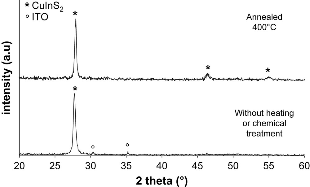
For electrodeposited films, an annealing treatment at 400 °C is necessary in order to obtain crystallized CuInS2 as presented in Fig. 4. Thin films prepared at room temperature and calcined at 200 °C are characterized by amorphous patterns. These results are in good agreement with those of Martinez et al. [13], who have shown that crystallisation of copper indium disulfide only begins at 300 °C during 1 h. As seen in Fig. 4, no peaks from other phases are present. Diffraction peaks at 28.0, 32.5, 46.5 and 54.7° correspond, respectively, to (112), (200), (220), (204) and (312) orientations.

XRD patterns of C and D series electrodeposited films.
3.3 Optical transmittance
To compare transmittance spectra, and absorption properties, of A–D samples, thickness variations of the different films have to be considered. Transmittance T was normalized with respect to film thickness t by Eq. (1):
| (1) |
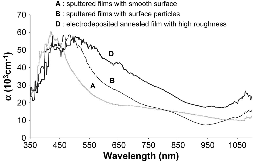
Absorption coefficient α versus wavelength A, B and D films.
4 Discussion
The deposition rates are very different for sputtered and electrodeposited films. The deposition rate varied from 2.5 to 6.4 nm/min for sputtering, depending on sputtering parameters, and was about 75 nm/min for electrodeposition. Both techniques lead to useful thickness for solar cell application (0.7–0.9 μm for sputtered films and 1 μm for electrodeposited films).
Calculated from XRD using Scherrer's formula, the crystallite size is about (50 ± 10) nm for sputtered films and about (70 ± 10) nm for electrodeposited films. This is in good agreement with AFM images: values about 50–100 nm and 70–150 nm are obtained for sputtered and electrodeposited films, respectively. This reveals nanostructuration of films and similar crystallite sizes for both techniques. However, electrochemical and sputtering techniques lead to very different surface morphologies: low-power sputtered films are generally smooth with an average roughness about 4 nm (Fig. 2a). In case of higher power and lower pressure the surface is covered by particles of 0.5–1.2 μm diameter (Fig. 1b). The number of surface particles increases with increasing deposition time. For electrodeposited films, the roughness is much higher and films are more porous (Fig. 2b). Films are more adherent as-deposited than after annealing, which is due to crack formation during annealing (Fig. 1e). Clearly, some strains in the as-deposited films are released during annealing at the expense of crack formation.
The structures are also different: sputtered films have crystalline chalcopyrite structure after deposition without any heating or chemical treatment (Fig. 3). Films are strongly oriented along the (112) plane. After annealing, some initially remaining amorphous phase crystallizes and other diffraction peaks appear corresponding to (220), (204) and (312) planes. Electrodeposited films are amorphous after deposition (Fig. 4), but chalcopyrite phase is obtained after annealing at 400 °C during 30 min, in good agreement with the literature. The (112) preferential orientation is not observed for electrodeposited films. The highly oriented structure of sputtered films might be interesting for electrical and photovoltaic properties. This has already been observed on chalcopyrite and particularly in the case of CuInSe2 films [21]. In this work, two different CuInSe2 structures were obtained by electrodeposition in pH-buffered and non-buffered solutions. Films obtained in non-buffered bath get strong (112) orientation and gave solar cells with 8.7% efficiency. Films obtained in pH-buffered solution with comparable thickness have random orientation and give solar cells with a lower efficiency of 3.1%. The difference is important for open-circuit voltage, short-circuit current density, and fill factor.
The different morphologies lead to different optical properties. High optical absorbance was obtained in the range of visible light and decreased with increasing wavelength for both sputtered and electrodeposited films (except amorphous electrodeposited films). This is in good agreement with the literature. Yunxia et al. [22] have obtained a high absorption coefficient in visible light for chemically deposited CuInS2 thin films, which decreased when reaching near infrared region. Similar transmission spectra were also obtained for highly oriented (112) films deposited by one-stage RF reactive sputtering [23].
Electrochemically deposited films have a higher absorption coefficient in a larger range of wavelengths than sputtered films. This high absorption is explained by the high roughness of the electrodeposited film, which reduces light reflection and increases light trapping. The light trapping effect is well known on strongly textured anodised silicon, where pores act like scatterers on the incoming radiation [24]. Even if chalcopyrite films have a higher absorbance than silicon, the same phenomenon occurs for both electrodeposited and sputtered films. According to this property, the film absorbance is proportional to the film roughness as verified in our experiments: the very smooth A samples present a lower optical absorbance.
Using the transmission spectra, the direct band gap of the semiconductor can be calculated from the absorption coefficient α with Eqs. (1) and (2):
| (2) |
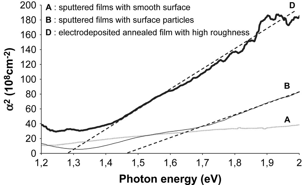
Band gap estimation for A, B and D films.
5 Conclusion
CuInS2 thin films were successfully prepared using both vacuum and non-vacuum techniques. Electrodeposition and sputtering lead to different morphology, structure and properties of films. Crystalline, strongly (112)-oriented chalcopyrite films were directly obtained by sputtering, and non-oriented films by annealing of electrodeposited samples. Rough surfaces were observed on electrodeposited and smoother ones on sputtered samples. A much higher deposition rate is obtained by electrodeposition and, considering the low cost of this technique, it seems to be suitable for large-scale production, but is restricted by the necessity of annealing. Furthermore, electrodeposited films present better optical properties for solar cell application than sputtered films, as seen by the calculated absorption coefficient, due to the high porosity of electrodeposited films. Electrical properties of sputtered and electrodeposited thin films and influence of the different morphologies and structures will be investigated in the future.