

1 Introduction
Solution processing of thin film materials is clearly a growing area of interest because of its ability to reduce the cost of the production of thin films. CuxS is an interesting material for its semiconducting properties. Indeed, the variation in x, 1 ≤ x ≤ 2, can provide a range of distinct crystalline phases depending on the temperature [1,2], producing significant variation in the electrical conductivity [3] and optical band gap [4]. The CuxS thin films have been found to possess near ideal solar control characteristics [5]. It is known that the short circuit current (Isc) is a function of x in CuxS for the CdS/ CuxS heterojunction. As x increases, Isc also increases and attains a maximum value at x equal to 2 [6]. Many methods have been developed to prepare Cu2S thin films, such as solid state reaction [7], chemical vapor deposition (CVD) [8], spray pyrolysis [9], chemical bath deposition (CBD) [10–14], microwave assisted chemical bath deposition [15] and successive ionic layer adsorption and reaction (SILAR) [16–18]. The CBD technique is well known as a prevalent low-temperature aqueous technique for deposing thin films, the simplest and the economical one. The CBD process uses a controlled chemical reaction to achieve thin film deposition by precipitation. In the present work, the effect of pH of the chemical bath on the physical properties of Cu2S thin films is studied. The as-deposited films are characterized for their structural, surface morphological and compositional properties. Electrical and optical properties are reported for the film exhibiting the best crystallinity.
2 Experimental and theory
Cu2S thin films are prepared by CBD method on corning glass slides (26 × 38 × 1 mm) and SnO2:F/glass coated substrates. The glass substrates are dipped during 5 min into hydrochloric acid and nitric acid, ultrasonically cleaned with double distilled water, immersed into methanol solution, rinsed again with double distilled water and then cleaned with hydrofluoric acid solution (HF 7%). Finally, the substrates are rinsed and stored in dried box during 15 min. SnO2:F/glass substrates are prepared by spray pyrolysis using SnCl4 (23 cm3), NH4F (5 g), methanol (970 cm3) and double distilled water (7 cm3). The substrate temperature is 440 °C and spray time is 10 mins [19].
The chemical bath used for the Cu2S thin films preparation is an aqueous solution of 5 ml of 1 M of copper chloride (CuCl2), 8 ml of ammonia (NH3 [28%]), 4 ml of triethanolamine (TEA), 6 ml of 1 M of thiourea (SC(NH2)2) and 63 ml of deionized water. The pH was 9.4. The preparation of the films is carried out with the same composition of the chemical bath where ammonium hydroxide and triethanolamine are used as complexing agents. NH3 was added to the chemical bath to adjust the pH from 9.4 to 11 under the control of a pH meter. The deposition time (tD) is constant and equal to 32.5 min [20] and the bath temperature is maintained at 40 °C. The formation mechanism of the film has been described as the slow release of sulfur ions from thiourea and then the combination with copper ions of TEA complex in an alkaline solution [21].
The as-deposited films are characterized for their structural, surface morphological, compositional, electrical and optical properties using X-Ray diffraction (XRD), atomic force microscopy (AFM), Auger electron spectroscopy (AES), Accent HL 5500 Hall system and optical spectroscopy measurements.
X-ray diffractions (XRD) are recorded with a Philips X’Pert X-ray diffractometer using CuKα monochromatic radiations. The wavelength, accelerating voltage and current are, respectively, 1.5406 Ǻ, 40 kV and 30 mA for 2θ values over 10–60°. AFM analysis is carried out with a Veecoo Dimension 3100 Atomical Force Microscopy using tapping mode. EDAX Study is performed using high resolution scanning electron microscopy EDAX XL 30.
Auger measurements is carried out with a Riber system equipped with a cylindrical mirror analyser (CMA) and working on the first derivative mode, the impinging current is 30 μA and the electron-beam cross section is 121 mV. The work function Φ of the film is obtained by the Kelvin method which allows us to determine the contact potential difference (Φ1–Φ2)/q between the surfaces of these samples. A metallic probe (work function Φm) vibrates in front of the investigated surface (work function Φ). By means of a compensation voltage, E, we equalize the surface potentials of the probe and of the sample and cancel the electric field, ɛ, between them. Then (Φ1–Φ2)/q = E. As ɛ = 0, there is no modification of Φ by the measurement technique and therefore, the compensation voltage yields the true value of (Φ–Φm).
The Hall measurements were performed using the five contacts Van Der Pauw method [22] with silver paints as contacts. The thermoelectric power was measured by using the four wires method developed by Bonnet et al. [23].
The optical properties were studied according to UV-VIS spectra with a UV-VIS-NIR spectrophotometer (NKD 7000). The optical absorbance is found by using the relation:
where A is the absorbance, R is the reflectance and T is the transmittance.
The extinction coefficient (k) and refractive index (n) are calculated by the following formulas:
3 Results and discussions
3.1 X-ray diffraction
Fig. 1 shows the XRD of Cu2S grown on glass substrates at different pH ranging from 9.4 to 11. The broad hump in the 2θ range of 15–35° is due to the glass substrate.
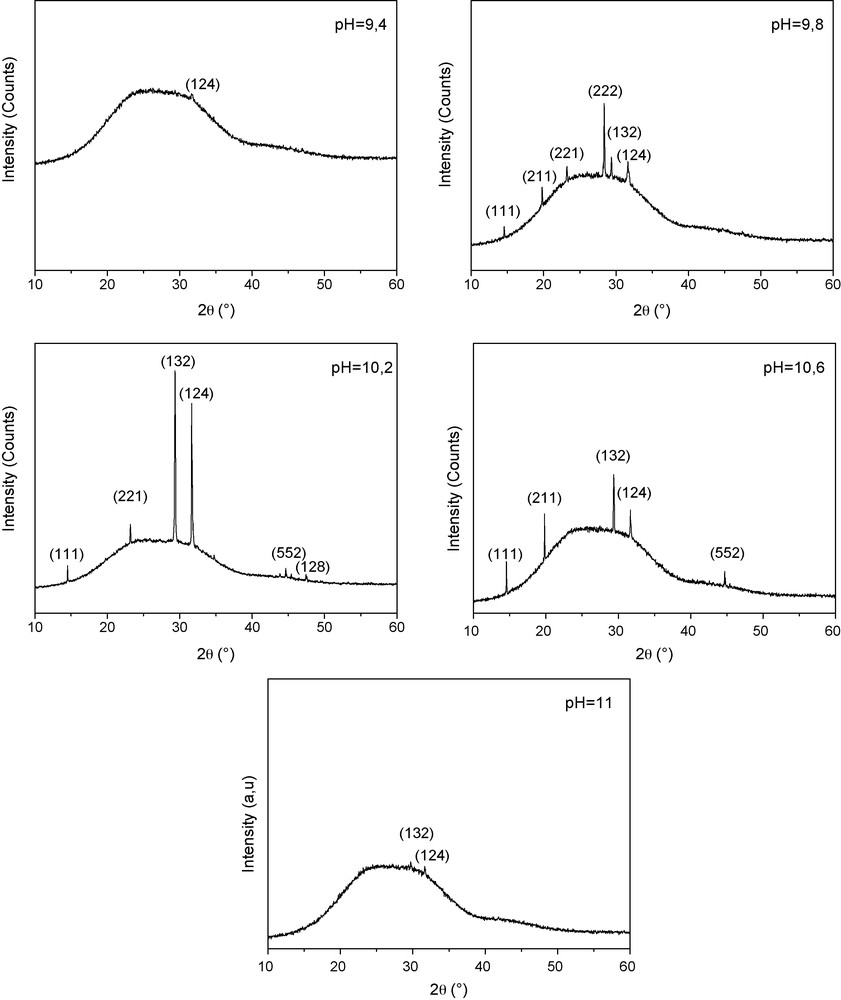
X-ray spectra of copper sulfide Cu2S thin films deposited on glass substrates at different pH solutions.
For both pH = 9.4 and pH = 11, the spectra show practically an amorphous Cu2S film (no diffraction peaks are present in both spectra). However, an improvement of the films crystallinity starts to appear, when the pH increases from 9.8 to 10.2. But, the quality of the films structure decreases with the pH increases from pH = 10.2 to 10.6 when the intensity of most diffraction peaks decreases. The best crystallinity is obtained for the Cu2S thin films deposited at pH = 10.2. Their crystalline structure exhibits peaks corresponding to (111), (221), (132), (124), (552) and (128) planes. These diffraction peaks are assigned to the monoclinic structure (Chalcocite). A preferential (132) orientation is observed for Cu2S films grown at pH = 10.2 and 10.6.
The average size of crystallite is estimated by Scherer's formula:
where λ is the X-ray wavelength of CuKα radiation (0.154 nm), k = 0.9 is the shape factor, θ0 is the Bragg angle and Δ(2θ) is the experimental full-width at half maximum of the respective diffraction peak. The average grain size for the Cu2S corresponding to the (132) orientation is about 60 nm.
3.2 Morphological characterizations
Fig. 2 shows two-dimentionnal (2D) and three-dimentionnal (3D) AFM scans of 4 μm2 of the crystallized Cu2S thin films grown by CBD on glass substrates at pH = 9.8, 10.2 and 10.6. The surface relief shows roughness and shaped crystallites. We note that the clusters size decreases randomly from pH = 9.8 to pH = 10.2 and then increases slightly from pH = 10.2 to pH = 10.6. It varies in the range of 0.1–0.3 μm for pH = 10.2.
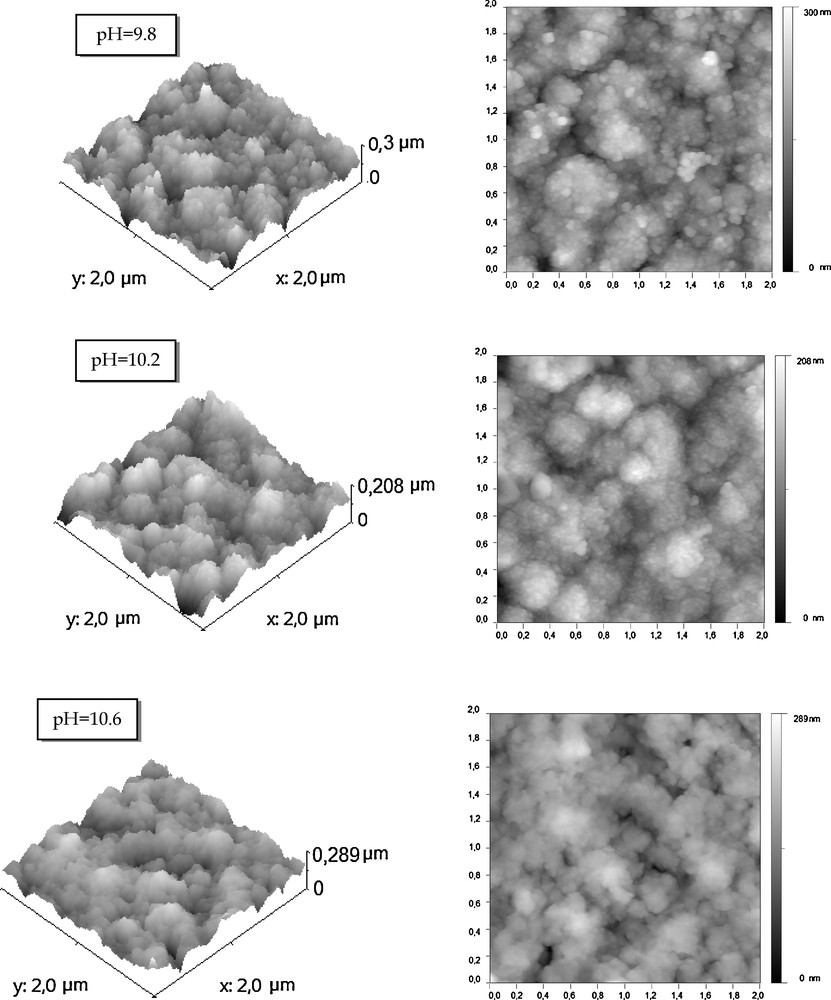
2D and 3D AFM images for crystallized Cu2S thin films grown on glass substrates at different pH values (pH = 9.8, 10.2 and 10.6).
The film prepared at pH = 10.2 appear quite smooth compared to those prepared at the other pH values. Indeed, the root mean square (RMS) of the roughness at different pH value of the Cu2S thin films prepared on glass substrates. We note that the minimum RMS value is about 30 nm at pH = 10.2 which reveal a better quality of the surface in this case. We can conclude that the pH value of 10.2 is the optimum value to the Cu2S preparation. This result is in agreement with the X-ray characterizations.
Cross-sectional SEM images of a typically obtained CuS2 layer show that average thickness of the layers is about 0.4 μm for a deposition time equal to 32.5 mins.
3.3 Surface composition
Auger studies are useful to get information on the surface layer composition and a comparative study allows identifying a possible contribution of some growth parameters to this surface composition. In this work, Auger studies are used to obtain quantitative information on the role of the pH solution and to deduce the main features of the surface layer. The Cu and S constituent elements, as well as Cl, C and O impurity elements, are found in the films AES spectra (Fig. 3). The oxygen may be incorporated into the film either from the atmosphere or from the aqueous medium of the bath solution. The source for carbon contamination may be due to the exposure of the samples to atmospheric conditions, and the laboratory environment in which samples are manipulated. The chlorine residue content shows some incomplete reaction between the precursors.
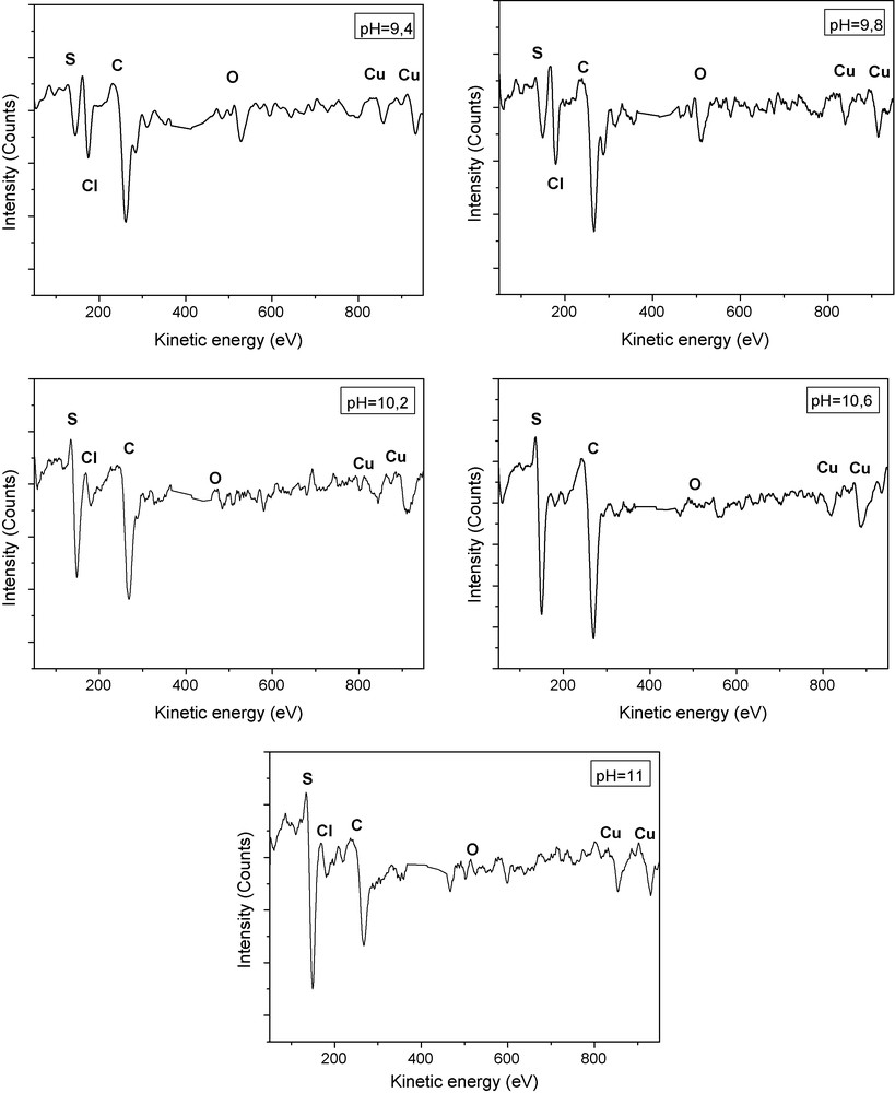
AES spectra of Cu2S deposited on SnO2/glass substrate for tD = 32.5 minutes at different pH solution of the chemical bath deposition.
From Fig. 3, it is observed that the O and the C Auger peak intensity decrease when the pH value increases. Also, we note that in the case of films grown at pH = 9.4, 10.6 and 11, the Cu/S atomic ratio decrease indicating that the amount of S is in excess at the film surface. As shown in Table 1, the best Cu/S ratio obtained is in the case of Cu2S thin films prepared at pH solution equal to 10.2 (Cu/S = 2.02) which is close to the stochiometric composition.
The Cu/S, Cl/S, C/S and O/S ratio for Cu2S thin films grown on SnO2/glass substrate for tD = 32.5 min at different pH values.
| pH | 9.4 | 9.8 | 10.2 | 10.6 | 11 | |
| Ratio | ||||||
| [Cu]/[S] | 1.84 | 2.1 | 2.02 | 1.76 | 1.60 | |
| [Cl]/[S] | 0.67 | 1.49 | 0.26 | 0.09 | 0.14 | |
| [C]/[S] | 11.19 | 7.35 | 3.63 | 3.78 | 1.49 | |
| [O]/[S] | 1.02 | 1.34 | 0.60 | 0.31 | 0.27 |
The quantitative composition of the Cu2S film grown on glass substrate for pH = 10.2 is also deduced from energy dispersive X-ray analysis (EDAX) technique provided by Scanning Electron Microscope. The atomic ratio of Cu/S is found to be equal to 2.01. These results confirm that Cu2S thin films exhibit stochiometric composition.
3.4 Work function measurements
The layers are characterized by a good stability: the work function and the surface photovoltage did not change with time. In all the cases, variation of ΔΦ with time were small; the uniformity of the surface layer (that is to say, the surface states, the stoichiometry, and the absorbed dipoles) is good. We studied the variations of ΔΦ with the pH of the Cu2S thin films grown on SnO2/glass for tD = 32.5 min. The results are summarized in Table 2. We note that the increase of the pH solution results in a decrease of the ΔΦ from +164 meV to −20 meV. We note that there is no photovoltage, so no surface barrier: the bands are flat.
Work function of Cu2S thin films grown on SnO2/glass substrate for tD = 32.5 min at different pH values.
| pH of the solution | 9.4 | 9.8 | 10.2 | 10.6 | 11 |
| ΔΦ (meV) | +164 | +150 | +145 | +45 | −20 |
3.5 Electrical properties
Hall effect measurements are implemented to characterize the electrical transport properties for the Cu2S thin layers. All films are p-type conducting. This result is in agreement with the literature [16–19,24,25].
For Cu2S thin films grown on SnO2/glass substrate at pH = 10.2, the resistivity, carrier density and mobility at room temperature are, respectively, 3.85 × 10⁻⁴ Ω-cm, −3.43 × 1020 cm−3 and 47.3 cm2/V.s.
3.6 Optical properties
The optical properties of the films deposited on glass substrates for tD = 32.5 min at the optimal pH value (pH = 10.2) are determined from the Absorbance (A), reflectance (R) and transmittance (T) measurements in the range 350–1000 nm. Optical measurement reveals that the maximum percentage transmission is 60.2% at λ = 630 nm [16], while the reflectance is lower than 15% in the visible range.
Based on the obtained optical transmission measurements, the square of absorption coefficient (αhν)2 is plotted as a function of photon energy (hν). A steep optical absorption feature is obtained, indicating that good homogeneity in the shape and size of the grains as well as low defect density near the band edge. As can be seen, (αhν) 2 varies almost linearly with hν above the band gap energy (Eg). Accordingly, the following equation for a direct interband transition can be applied [26]:
The band gap energy (Eg) is 2.37 eV, which is in agreement with value reported earlier for Cu2S films [16,27].
The variation of extinction coefficient (k) and refractive index (n) with the incident photon energy (hυ) are determined. We note that (n) and (k) vary in the range of 1.7–2.1 and 0.02–0.09, respectively.
4 Conclusion
Cu2S thin films are prepared on glass and SnO2/Glass substrates by the chemical bath deposition technique. The depositions are carried out during 32.5 min in the pH range from 9.4 to 11. The thickness of the films is about 0.4 μm. X-ray diffraction study shows that the film structure depends on the pH value. In fact, as-grown films are amorphous for pH = 9.4 and 11, however, the best crystallinity of Cu2S thin films is obtained for pH equal to 10.2. The crystallized thin films exhibit a monoclinic structure. In addition to X-ray results, Auger and AFM studies confirm that pH = 10.2 is the optimum value to grow Cu2S thin films. Indeed, thin films grown on SnO2/glass substrate exhibit stochiometric composition with [Cu]/[S] concentrations ratio equal to 2.02 and quite smooth surface compared to those prepared at the other pH values.
Those films revealed a direct band gap of about 2.37 eV and have a p-type electrical conductivity with a resistivity in the order of 3.85 × 10⁻⁴ Ω-cm at room temperature. The refractive index (n) and the extinction coefficient (k) vary in the range of 1.7–2.1 and 0.02–0.09 respectively.
The optical properties of such films make them suitable for solar control coatings and photovoltaic devices. From the point of view of commercial-scale production, chemical bath deposition of Cu2S thin films on SnO2/glass substrate is expected to be promising for large area film deposition at a relatively low-cost production.
Acknowledgments
The authors wish to thank the comité mixte de coopération universitaire (Tunisia-France) for financial support under the project number 07S1304, as well as Égide France under the project Hubert Curien - Utique number 15385QG.