

1 Introduction
Mobile analyte-specific gas sensing is a very important research topic and business in many fields such as technical, environmental, automotive, medical, and security applications. Explosives have to be found, the concentration of dangerous and/or air-polluting gases has to be monitored, and vegetative indicators have to be surveyed in order to prevent harm. For example, in the medical sector it is necessary to monitor and control respiratory gases. Ethanol breath testing is a common example, too. Several types of microstructured gas sensors are available on the market. These microstructured gas detectors measure typical the changes in the conductance or in the capacitance induced by the presence of certain gas atoms that are adsorbed onto the surface or which diffuse into the detector material. These sensors are typically applicable only to certain specific gases that influence the physical properties of the detector materials and suffer from non-specific binding of molecules to the surfaces. Here we report on two analyte-specific working principles for microsensors and the thermal emission properties of 2D silicon photonic crystals.
1.1 Optical gas sensing
Optical or, more specifically, spectroscopic gas sensors, measure the change of reflection or transmission in the presence of gases in the ppm and upper ppb range. Characteristic absorption lines arising, e.g., from rotational and vibrational excitations of the molecules in the mid-infrared (MIR) spectral range are monitored. The spectroscopic principle is a rather general approach applicable to a broad variety of gases, and in addition it is highly selective due to the specific rotational-vibrational states (fingerprint) of every gas. The major drawback of such optical sensors is their relatively high cost due to the high demands on the optical components.
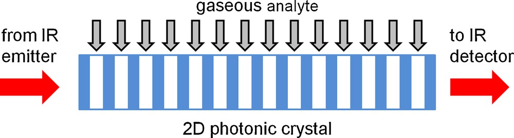
A conventional spectroscopic gas sensor consists of three basic parts: the radiation source, the interaction volume, and the radiation detector. Using, e.g., laser sources and adapted detectors, very sensitive, selective, and fast instruments can be built [4–6]. Employing tunable laser spectroscopy, a monochromatic intense laser emission line is precisely tuned across gas absorption lines. Highly collimated laser beams can be combined with efficient Harriott multi-reflection cells, yielding interaction lengths of 100 m and above [5]. Thus, e.g., with quantum cascade lasers (QCLs), in the MIR range, sensitivities in the parts per trillion range can be achieved. Using cavity ringdown or cavity leak out setups, effective interaction lengths of several kilometers have been demonstrated that also yield ppt sensitivity. However, in most cases the high price of the lasers and other system components is prohibitive and limits these techniques to niche applications. For the majority of optical gas sensors, low-cost thermal emitters and thermopile or pyroelectric detectors are used in sensors with adapted optical components. Therefore, we focus our work on this case. We suggest the use of photonic crystals (PhCs) to obtain compact, robust, and low-cost spectroscopic microsensors. We consider the replacement of the interaction volume only in such a conventional sensor by a PhC as shown in Fig. 1.
Schematic diagram of a typical PhC gas sensor. The light impinging from the left side is absorbed by the gas molecules inside the PhC. The reduced group velocity results in an enhanced interaction length and allows the physical reduction of the sensor.
Due to the dilute nature of gases, their interaction with light is rather weak (as compared to that of liquids), which in turn necessitates relatively long interaction paths in the range of 10 to 50 cm in order to determine concentrations in the ppm range [7]. Such long interaction paths and therefore large interaction sample volumes result in relatively large sensor devices. This is both impractical and it is often impossible to fill such large volumes with gas, as in, e.g., the case of baby breath monitoring. Furthermore, it is usually necessary to keep the interaction volume at a certain temperature in order to avoid condensation and to guarantee reproducible measurement conditions. This is energy consuming, especially for large volumes.
A reduction of the interaction volume can be achieved by increasing the effective interaction of the radiation and the gas. Here, we suggest a device based on a silicon PhC. The basic idea is that an effective interaction path of light with an analyte of 10 to 50 cm can, in principle, be obtained by using low group velocity modes in a PhC of less than 1 cm in size. Furthermore, silicon enables the integration of devices, and the thermal drift is greatly reduced as compared to a classical gas cell with multiple path interference.
The working principle underlying a PhC-based spectroscopic gas sensor is the enhancement of the interaction among the radiation and the gas molecules. This enhancement can be achieved by prolonging the interaction time tint = lint/vg, between the radiation and the gas, given by the ratio of the interaction length lint to the group velocity vg. The interaction of radiation and gas molecules can be described by the Lambert–Beer law of absorption, .
It states that the intensity I(lint) after the interaction of light and gas along an interaction path of length lint is given by the transmitted intensity I0, measured without gas present, times an exponential decay determined by the absorption constant α of the gas, the concentration of the gas c, and lint. In a PhC, the physical interaction length required to achieve the same absolute absorption is therefore made smaller by the enhanced absorption that can be achieved due to the low vg.
A PhC-based spectroscopic gas sensor has to fulfill the following requirements: the energetic band structure should have a low group velocity region that spectrally overlaps with the absorption frequency of the gas (resonance condition). The symmetry of this resonant band has to allow coupling to impinging and outgoing plane waves (symmetry condition). And the electric field of the chosen mode should be located mostly within the pores of the PhC (interaction condition).
To fulfill the resonance condition, flat bands have to be chosen. Flat bands in the photonic band structure of a 2D PhC are, e.g., found at the high symmetry points of the band structure. To meet the interaction condition, we select so called air bands, where the energy is located in regions of the PhC having a lower refractive index. Because scattering losses by the upper edge of the photonic band structure increase in higher bands, the lowest bands fulfilling these conditions are the second TE band and the third TM band in the Γ-K direction which will be used in the following.
However, there is a drawback with such a simple PhC gas sensor. In a classical picture, a low group velocity vg corresponds to a high refractive index neff. This makes the in- and outcoupling of radiation difficult. This problem could be overcome by the design of an appropriate taper or an anti-reflection layer (ARL), taking into account the impedance and the modal mismatch. This can be realized in 2D by using specially designed surface modes that couple with very high efficiency plane waves to low vg modes [8].
1.2 Gas ionization
To date the security screening instruments of choice are ion mobility spectrometers (IMS), which are basically time-of-flight mass spectrometers. Widespread adoption of the IMS technology in civilian security screening applications, for instance, at airports, has been hindered due to the fact that state-of-the-art spectrometers employ radioactive ion sources. To replace these unwanted ionization elements, either laser ionization or surface ionization is possible. For the latter high electric fields are required. Therefore, field enhancement at sharp conductive tips is suited for surface ionization. The ionized molecules will then enter the flight time analyzer. A proof of principles has been shown using focused ion beam deposition of the platinum nanotips [2]. Because this is neither cost- nor time-effective for large scale electrodes, there is a need of a process to fabricate large areas of well defined and ordered tip arrays (to achieve homogeneous field enhancement).
1.3 Thermal emission of photonic crystals
Two dimensional (2D) photonic crystals provide a wide range of applications due to their good compatibility with classical integrated optics and rather simple fabrication processes compared to 3D PhCs. Based on the photonic band structure, the photonic density of states (DOS) inside the photonic crystal provides some interesting regions like slow modes near the band edges or no states inside the gap regions which could be useful to control the thermal radiation. From a thermodynamical point of view, the selective thermal emission will not be stronger than that of a black body [9]. However, due to the lower integrated spectral emissivity, a lower power consumption is expected compared to a blackbody which is advantageous for mobile, energy-saving sensing application.
We report on the spectral modification of the thermal emission of 2D and 3D silicon photonic crystals compared to bulk material by heating the photonic crystal directly by DC currents and passively with external hotplates [3].
2 Fabrication of the silicon microstructures
Photo-electrochemical etching of n-type silicon in HF with lithographically predefined pore positions has been used for, e.g., 2D silicon photonic crystals [10,11]. By appropriate control of the backside illumination and bias voltage, the diameter of the pores can be varied during the etching process. This has been used to create 3D periodic structures such as photonic crystals [12]. For the two types of gas sensors described here, we have to etch a membrane structure on the one hand and on the other hand a nanotip structure.
2.1 Membranes
The etching process was optimized to achieve membranes with optical smooth side facets and directly integrated anti-reflection layer (ARL) within a single process [13]. The PhC regions, the trenches, and the ARL regions were predefined by photolithography and were transferred by photo-electrochemical etching into the silicon wafer. The lattice constant used was a = 2 μm, and the radius varied slightly between r/a = 0.36 and r/a = 0.385. The radius variation was carried out to match the gas absorption wavelength. The width in the direction of the propagation of the light of the PhC samples was 0.1, 0.25, 0.5, and 1 mm, corresponding to 50, 125, 250, or 500 PhC lattice constants. Through detailed control of the etching current, straight pores 330 μm in depth were prepared and detached from the substrate by increasing the current density above the electro-polishing regime. This one step process led to single membrane devices with a thickness according to the pore depth (Fig. 2).
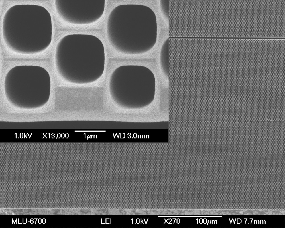
SEM picture of a complete 0.25 mm PhC gas cell device. The insert shows the coupling layer (ARL) at the interface with the PhC.
2.2 Sharp tips
To create sharp micro-tips at the surface of a n-type silicon wafer the etching process was altered. By using an ordered hexagonal pore layout, the distance between every two adjacent pores is equal to the lattice constant a. The r/a-ratio is defined by the ratio between the pore distance a and the pore radius r. If we increase the r/a-ratio during the etching process, the pore sidewall thickness decreases until the pores touch each other at r/a = 0.5. At the whole surface will be covered by overlapping pores without resisting silicon. By starting the etching process with and decreasing the r/a-ratio, single tips are formed in between three adjacent pores each. Compared to other tip-etching techniques like anisotropic etching for example [14] the aspect ratio and even a more complex profile for the tip geometry is possible with this electrochemical process. The diameter of the tip can be dynamically controlled along the length axis of the tip so that low aspect ratio tips (Fig. 3) as well as high aspect ratio tips are possible with the same process and material parameters.

Scanning electron micrograph: top: additional tip sharpening results after different steps of thermal oxidation + HF dips. Bottom: needle shaped tips with high aspect ratio and covered with platinum for surface ionization (insert).
By applying additional thermal oxidation and oxide removal steps after the photo-electrochemical etching process, the quality of the tips can be improved. Another benefit of the oxidation is that oxidation at lower temperatures (T < 950 °C) leads to a decreased curvature radius.
As far as the scanning electron microscope image can show, curvature radii of rc ≤ 10 nm which is sufficient for a large field enhancement effect can be achieved after just two oxidation steps at low temperature. To functionalize the silicon tips for increased ionization or electron emission rates, the tips have to be covered with the different materials according to the specific application (e.g. thermal or coronal ionization).
3 Measurements
3.1 Optical transmission measurements
Following the technology described above, 2D PhC samples with optical path lengths from 100 μm to 1 mm were obtained. The height (i.e. the pore length) was 300 to 400 μm and the width of the samples 1 mm. Optical transmission measurements without any gas were carried out to measure the intrinsic losses of the PhC devices depending on their length. A target wavelength of 4.24 μm was used in order to meet the test absorption frequency of CO2. A broadband thermal emitter from Intex was modulated with 10 Hz and filtered by a 4.24 μm bandpass filter. Due to the small size of the PhC, a pinhole of typically 100 μm was used in front of the PhC device. An edge filter consisting of a sapphire window was placed in front of the pyroelectric detector (Fig. 4). The signal of the detector was measured with a lock-in amplifier.
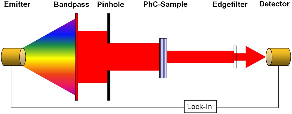
Schematic diagram of the optical transmission setup. Light from a broadband thermal emitter is passing through a bandpass filter with a center wavelength of 4.24 μm and a 100 μm pinhole. Light transmitted through the PhC and the following edge filter is detected by a pyroelectric detector.
Transmission measurements with this setup typically indicate a transmission of about 10% for an optical path length of 100 a and about 3% to 4% for 500 a, corresponding to an attenuation of about 15 dB/mm. The high losses are probably due to residual scattering. SEM analysis of the pore diameter variation yields an average value of 1% to 2%, mainly due to doping variations in the starting silicon material. The pore positional variations are negligible due to the resolution of the photo-lithographical process. To estimate the impact of scattering on the transmission properties, we used the finite-difference time domain (FDTD) method to simulate the transmission of a perturbed PhC in the spectral region of 0.35 < a/λ < 0 by varying the average pore radius by 1% using a Gaussian radius distribution. It turns out that this 1% pore diameter fluctuation yields easily to an attenuation in the transmission of 15 dB/m.
3.2 Gas sensing measurements
In the following, gas sensing experiments are presented with CO2 as a model analyte. In the gas cell, the PhC membranes are positioned between two BaF2 light guiding rods (12 mm × 1 mm × 400 μm), which couple the IR radiation in and out of the PhC sample. The rods are fixed within a groove (20 mm × 1 mm × 400 μm) and can be adjusted for varying optical path lengths of the PhC samples. A flat plastic top plate seals the setup so that it is airtight. Two tiny holes in the center at the position of the PhC enable a gas flow through the PhC along the pores. A schematic view is shown in Fig. 5.

Schematic design of the optical setup used for gas absorption measurements. The setup shown in Fig. 4 is complemented by a gas cell. The PhC membranes are positioned between two BaF2 light guiding rods. The gas analyte flow is perpendicular to the light path through the PhC membrane.
The assembled gas cell is mounted between a thermal radiation source and a pyrodetector with an IR bandpass filter centered at 4.24 μm for CO2. No further optical elements are necessary for this compact setup. The radiation intensity of the IR emitter was modulated via the operating voltage with a frequency of 10 Hz. The signal of the pyrodetector was measured using a digital lock-in amplifier with a time constant of 2 s.
In the course of the experiments, the gas cell was filled alternating with dry N2 and CO2. After the measurement of a sample, the PhC could be removed from the plastic holder without changing the positions of the BaF2 rods. Thus, measurements of the empty cell with the same optical path length were possible.
The results are shown in Fig. 6 in absolute values (a) and normalized to the same transmission without gas (b). In Fig. 6a, the IR absorption of CO2 is obvious. The transmission of the PhC sample (optical path length: 250 μm; membrane thickness: 330 μm) is only 8.6%. Initial measurements using other samples with PhC length of 1 mm yielded transmission values of approximately 4%. The data in Fig. 6b, normalized for the transmission, show that with the PhC the absorption by CO2 leads to a transmission change of 53%, whereas the cell without the PhC has a change in transmission of about 28%. Therefore, the nonvolume corrected sensitivity of the PhC is about twice the value of the empty cell. Taking into account the porosity of the sample of about 0.64, an overall absorption enhancement of a factor of 3 is obtained. Repeating this result for different sample lengths between 0.25 and 1 mm leads to absorption enhancements in the range of 2.6 to 3.5. This is evidence that enhanced absorption can be achieved in bulk PhCs. If we compare our results with our simulations we see a good agreement. Our measurements were carried out around a/λ = 0.47. In this region, a theoretical enhancement is far away from the working point, with the highest enhancement around a/λ = 0.40, and is dominated by the normal group velocity of about vg/c = 2 due to the effective refractive index of the silicon PhC. For our lattice constant of a = 2 μm, with a maximum enhancement corresponding to a wavelength of 5 μm, no absorption lines of suitable gases exist.
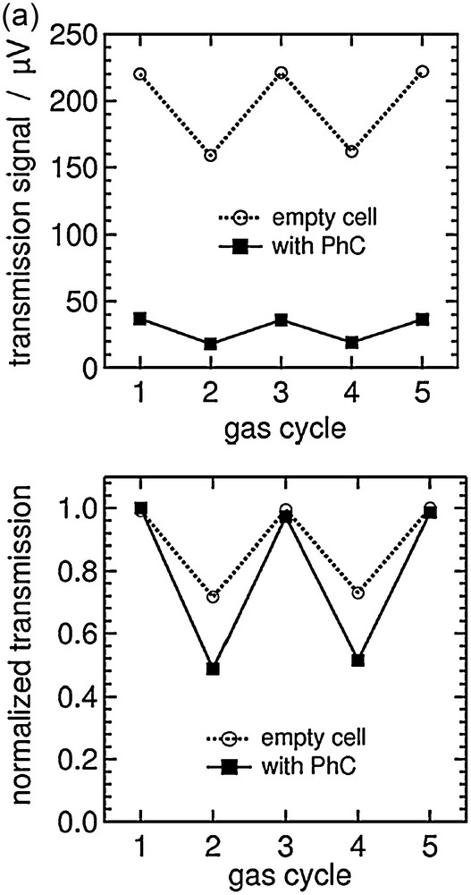
a: infrared transmission signal at 4.24 μm of the empty gas cell and the cell with a PhC sample 250 μm in length during gas filling cycles with N2 (cycles 1, 3, and 5) and CO2 (cycles 2 and 4); b: normalized transmission of the empty gas cell and the PhC sample.
The experimental enhancement factors fluctuate in a range of approximately 26%. This is caused by some uncertainties: The fluctuations originate most probably from slightly different orientations of the sample in the cell. This leads to a slight variation of the operation point and, therefore, to a variation of the group velocity. In addition, the coupling efficiency between the thermal emitter and the PhC is very low. Due to the loss of 15 dB/mm, the effect of a variation in coupling efficiency on the transmitted power is strong.
3.3 Ion current measurements
First preliminary measurements with ultra-sharp silicon nanotips have been made to investigate behaviour of platinum coated nanotip arrays. Platinum seems not to be suitable due to its limited thermo-mechanical adhesion properties on silicon. Preliminary ionization measurement with a platinum coated nanotip electrode at temperature between 600 and 750 °C for ethene and hydrogen confirmed the enhanced generation of positive gas ions on the microstructured silicon surface. However, the reduction of activation energy for surface ionization in the case of ethene is only from 3.2 eV for flat platinum electrodes to 2.8 eV for platinum coated silicon needles. The lower than expected reduction of the surface ionization energy is probably due to an insufficient covering of the nanoneedles with platinum.
3.4 Thermal emission measurements
The lattice constant (pore to pore distance, hexagonally arranged) of the photonic crystals was a = 2 μm and a = 4.2 μm and pore radius was nominal 800 nm and 1.7 μm (100%) respectively. The samples were used as membranes with 400 μm thickness in such way that the pores range from one side of the membrane to the other like open channels. Sample emission spectroscopy was carried out using a Fourier-transform infrared spectrometer (FTIR) Bruker IFS 66 with an additional channel for external light source characterization. Surface emission has been measured at different heating currents normal to the 4.0 mm × 4.7 mm probe surface. As reference, a similarly sized bulk-silicon sample was taken. Thermal emission was measured longitudinal (parallel to the crystal pores) as well as transversal (perpendicular to the pores, normal to the side face).
For the in-plane emission measurements an IR microscope was used to couple the probe emission into the FTIR spectrometer. With the additional apertures we were able to decrease the spot size down to several tens of microns. The exact position of the spot on the etched side face of the PhC structures can be controlled in the visible range. This enables us to collect thermal emission from the photonic crystals sideface perpendicular to the crystal pores, in-plane of the 2D photonic properties of the samples (Fig. 7).
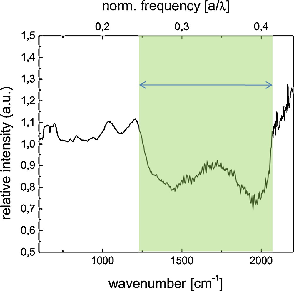
Relative thermal in-plane (perpendicular to the pores) emission spectrum of a silicon PhC membrane (a = 2 μm) relative to a bulk silicon sample.
Due to its large surface, covered with native oxide, the PhC structures show an increased emission intensity around 1100 cm−1, in accordance to a vibrational Si–O band. Consistent with the simulated 2D band structure, the out-of-plane measurements also show decreased emissivities at bandgap frequencies between 1250 cm−1 to 2000 cm−1 for the 2 μm structures. The PhC seems to work as a filter function for bandgap frequencies.
For out-of-plane emission measurements the PhC was electrically contacted at both sides and heated via DC currents. To verify the influence of the 2D photonic band structure on the out-of-plane emission spectrum, samples with different lattice constants were used. Compared to the thermal emission of bulk silicon the measured out-of-plane emission spectra of a 2D periodically structured samples show a sharp emission peak around 1100 cm−1 (Fig. 8) (top) and suppressed emission at higher frequencies. Whereas the maximum of the emission of a blackbody shifts with temperatures according to Wien's displacement law (Fig. 8) (top) the highly selective emission of the porous sample leads to a fixed peak at common temperatures. By measuring the emission spectra of crystals with different lattice constants, it is verified that the peak emission of the out-of-plane emissivity is not affected by the lattice constant and thus the in-plane photonic band structure (Fig. 8) (bottom).
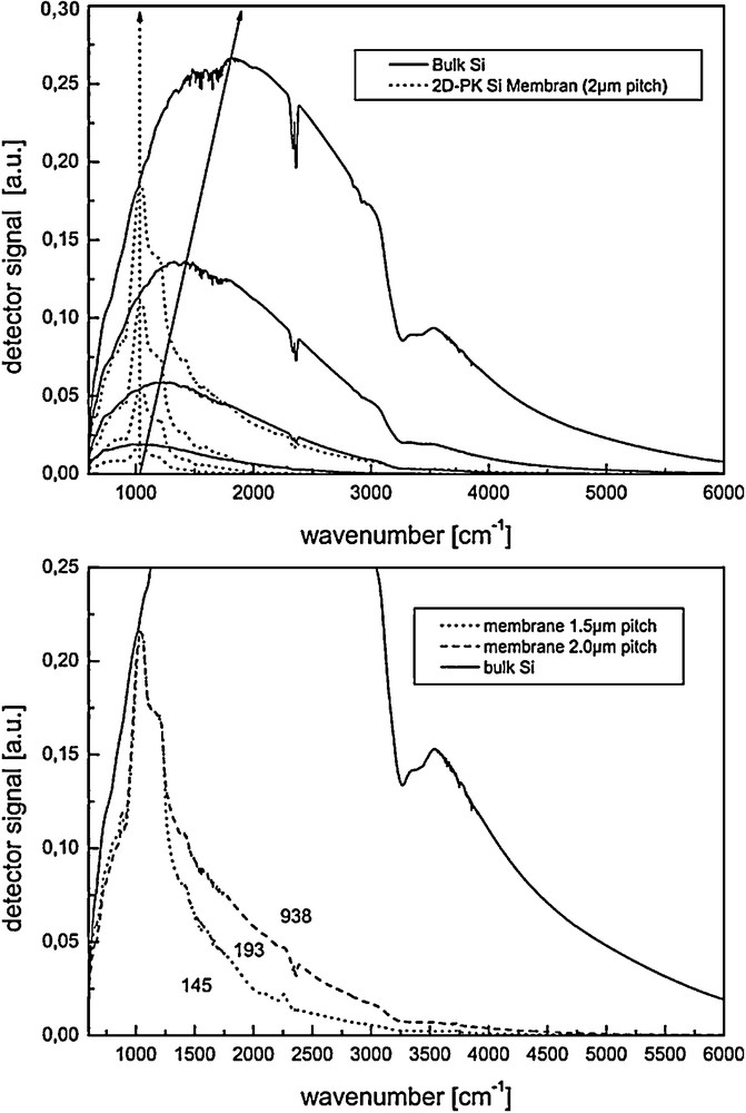
Out-of-plane (parallel to the crystal pores) emission measurements of 2D silicon PhCs compared to bulk silicon emission. Top: thermal emission spectra compared to bulk silicon samples for different temperatures. Bottom: emission spectra for crystals with different lattice constants compared to bulk silicon emission. For comparison, the integrated area below each spectrum is inserted in the diagram.
The strong selective emission can be explained by the enhanced silicon oxide surface emission of the inner pore sidewalls. The measured peak is in accordance to a vibrational Si–O band. Due to the high silicon oxide ratio caused by the porosity, the oxide emission dominates the emission spectrum [3].
4 Discussion
We have shown three concepts for silicon based spectroscopic microsensors.
In the case of the slow light optical silicon sensors, enhancement factors of about three to four have been shown experimentally. Based on theoretical considerations, enhancement factors of up to 60 for one polarization are possible [1]. The difference between the theoretical absorption enhancement factor and the experimental value results from the non-optimal lattice constant of our device. Therefore, our device is working slightly off-resonance, and the experimental enhancement factor is limited. Repeating the measurements with another gas instead of CO2 (e.g., OCS with absorption lines at 4.9 μm) should lead to a better agreement between theory and experiment. Moreover, the main reason for the high attenuation of about 15 dB/mm, the global pore diameter variations, can be attributed to doping inhomogeneities. These inhomogeneities of a Si wafer induce concentric striations at the etched surface caused by diameter variations of the pores. The global pore diameter fluctuation is 3.5%, and the local fluctuation is 0.8%. These fluctuations might be reduced by about 40% by using neutron-transmutated doped silicon or by using other etching techniques [15]. From our numerical simulations using perturbation theory, we estimate that for a transmission above 90% of a device 1 mm in length, the pore positional variation has to be below 0.3% and the pore diameter fluctuations have to be below 0.5%. This will remain a major challenge in the future.
In the case of ion mobility spectrometers, we have shown that thermally activated surface ionization of platinum coated microneedles arrays leads to a measurable enhancement of positive gas ion current. Currently the enhancement for our silicon microneedles arrays is limited by the conformal coating of a conductive platinum film. Theoretically, enhancement factors of more than 100,000 should be possible if the whole surface would be covered compared to flat surfaces. Atomic layer deposition of Iridium or Platinum seems to be a promising candidate for achieving this.
In the case of selective thermal emission we observed decreased emissivity within band gap frequencies. This is, however, only possible when there is a temperature gradient on the sample as expected from our measurement setup. If the whole crystal would be on exactly the same temperature, there would be no filter effect due to equilibrium of absorption and reemission. Only a grating effect (diffraction) of the external photonic crystal patterning would be observable. This assumption is supported by the out-of-plane measurements on 2D photonic crystals where no bandgap effect is present (Fig. 7). Instead we observe a strong emission of the silicon oxide covering the pore walls. The photonic crystal just acts like a filter for thermal emission.
5 Conclusion
Periodic silicon microstructures fabricated by photo-electrochemical etching are suitable spectroscopic microsensors. The flexible photo-electrochemical etching of silicon allows the production of macroporous membranes with pores of hundreds of micrometer length as well as super-sharp tips with curvature radii of only some nanometers.
The concept of gas sensors based on the classical non-dispersive infrared technique using thermal emitters and ultra-compact PhC gas cells was demonstrated. Enhancement of the CO2 infrared absorption by a factor of 2.6 to 3.5 as compared to an empty cell was observed due to slow light inside the PhC; this is in excellent agreement with numerical simulations. Theoretically, for an optimal design, enhancement factors of up to 60 are possible in the region of slow light. However, the overall transmission of bulk PhCs, and thus the performance of the device, is limited by fluctuations of the pore diameter. Numerical estimates suggest that the positional variations and pore diameter fluctuations have to be well below 0.5% to allow for reasonable transmission in a 1 mm device.
We have shown that the photo-electrochemical etching process in combination with thermal oxidation is a suitable process for cost- and time-effective fabrication of large scale nanotip arrays which fulfill the requirements for the enhanced ion generation. The limiting factor is currently a conductive coating of these microneedles by e.g. platinum. This novel route of microsystem technology integration of IMS might enable apart from security applications also new areas of application such as mould detection or food chain management monitoring.
We carried out a detailed study to understand the thermal emission properties of 2D silicon photonic crystals. It turned out that we do not see any features of the 2D in-plane band structure in the out-of-plane emission spectrum of pure 2D photonic crystals. However an enhanced emission peak of the thermal silicon oxide could be observed and explained by the highly porous structures.
Acknowledgments
We gratefully acknowledge financial support from BMBF (project PHOKISS 13N8525 and NACHOS 03X0010C) and collaboration with the Drägerwerk AG (A. Lambrecht) as well as EADS Deutschland AG (A. Hackner and G. Müller) in this project.