

1 Introduction
The precise control of the primary structures of metal nanoparticles, such as size, shape or composition, enables us to fabricate the secondary structures of nanoparticles, which means the regularly ordered metal nanoparticles with well-defined one- (1D) and two- (2D) dimensional spatial configuration. Since such ordered metal nanoparticles, so-called superlattices, are expected to show the novel properties that are not present in the isolated nanoparticles, the current interests in colloid chemistry have been focused on the fabrication of superlattices of size- and shape-controlled metal nanoparticles, as shown in Fig. 1 . The fabrication of ordered metal nanoparticles would enable us to produce the optical devices, such as surface enhanced Raman scattering (SERS) films [1,2], optical grating [3], antireflective surface coating [4], selective solar absorbers [5], and data storage devices [6]. Moreover, the monodisperse metal nanoparticles have potentiality to be the building blocks for nanoelectronic devices using the single electron tunneling effect [7,8]. Especially, the metal nanoparticles smaller than 2 nm in size are required for such devices to make use of the phenomenon of Coulomb blockade at room temperature [8–14].

Schematic illustration of metal nanoparticle superlattices.
To order the metal nanoparticles on substrates by evaporating the solvent from the nanoparticle solutions, one has to use the rigid stabilizer such as ligand or surfactant for metal nanoparticles to form nanoparticle superlattices of well-defined configurations, because the volume change of stabilizer like linear polymer through the evaporation of the solvent may suppress the complete arrangement of nanoparticles. In fact, 2.6-nm polyacrylonitrile-protected Au nanoparticles formed only a partially hexagonal network in two-dimension [15]. Two approaches have been employed in order to form superlattice structures of metal nanoparticles. One is to self-assemble metal nanoparticles by placing a few drops of their solution on a substrate or by dipping it into the solution, followed by the solvent evaporation. The self-assembly technique is a widely used fabrication method of superlattices due to its easiness and convenience. As indicated by Bowden and co-workers, the self-assembly technique has a great potential to produce the complex patterns of metal nanoparticles by endowing the nanoparticles with the direction of interaction [16]. Another approach is to use either external forces, such as an electrophoretic deposition [17,18] and a LB technique [19,20], or strong interactions, such as an electrostatic interaction [21–24] and a DNA hybridization [25–27]. Thus, we can learn the novel nanoscience of nanomaterials through nanotechnology.
Here the fabrication techniques and electronic properties of Au nanoparticle superlattices are presented.
2 Two-dimensional superlattices of gold nanoparticles
The fabrication of 2D superlattices of metal nanoparticles has been vigorously studied during a decade. The preparation technique mainly involves a self-assembly of organic ligand-protected metal nanoparticles larger than 2 nm. Since such nanoparticles are easily self-assembled in an hexagonal packing on various substrates due to the capillary force between the nanoparticles during the solvent evaporation, there are too many studies to mention [1, 2, 28–39]. On the other hand, when one uses 2D superlattices of metal nanoparticles as nanoelectronic devices making use of Coulomb blockade phenomenon at room temperature, metal nanoparticles smaller than 2 nm in diameter are required. In this section, the methods to fabricate 2D superlattices of Au nanoparticles larger and smaller than 2 nm are presented together with the techniques to control the particle sizes.
2.1 Fabrication of 2D superlattices of large Au nanoparticles
Needless to say, precise control of particle size and shape is required to fabricate their well-defined superlattices without mosaic structures. In 2001, we developed a simple and quite useful method to manipulate the size of Au nanoparticles by using the heat-treatment of small Au nanoparticles not in solution [40,41] but in the solid state [42,43], which is far from the conventional techniques [44–48]. A preparation of dodecanethiol-protected Au nanoparticles (DT-Au) as a source for the heat treatment followed the Brust’s two-phase (toluene/water) reaction procedure [49]. The organic (toluene) phase was then separated, evaporated completely in a rotary evaporator at 40 °C, and dried in vacuo at 30 °C for a day. The crude solid obtained was heat-treated at 150–250 °C at the heating rate of 2 °C min–1, and held for 30 min. The heat-treated product was dissolved in a small amount of toluene and mixed with methanol to remove excess free dodecanethiol and TOAB. The dark brown precipitate was filtered off, washed with methanol, and redispersed in toluene. Octadecanethiol (ODT) was also used as a protective agent in place of dodecanethiol. This heat-treatment of as-prepared DT-Au nanoparticles at 150, 190 and 230 °C led to the thermodynamical particle growth, the particle sizes becoming 3.4 ± 0.3, 5.4 ± 0.7, and 6.8 ± 0.5 nm, respectively. As shown in Fig. 2 , their UV–vis spectra displayed surface plasmon absorptions at around 520 nm. These results indicate that the smaller nanoparticle has the lower melting point and the nanoparticles grow uniformly until they become stable at the heat-treatment temperature. As Maye et al. pointed out [41], an evolution of the small Au nanoparticles proceeds via sequential DT desorption, Au core coalescence, and DT re-protection. During the heat-treatment process, TOAB melted is thought to serve as a solvent in the particle growth process, because the uniform growth of nanoparticles was not observed without TOAB molecules. The Au contents increased from 79.7 to 94.7 wt% with an increase in the heat-treatment temperature, i.e., with the size, which is originated from a decrease in the surface area of Au nanoparticles.
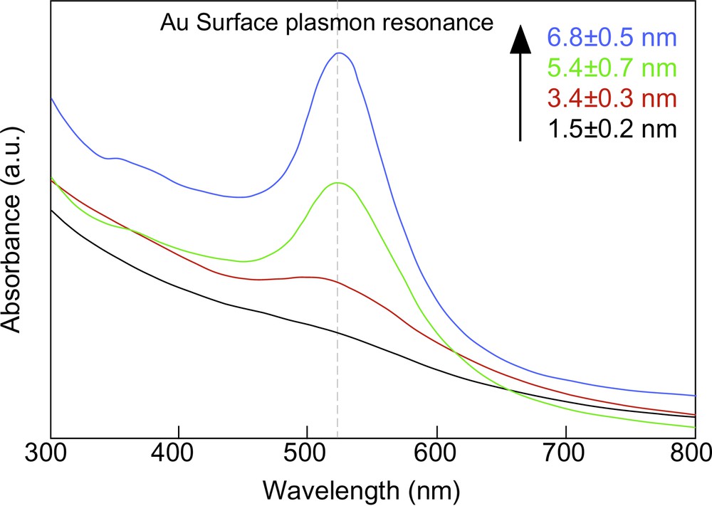
UV–vis absorption spectra of DT-Au nanoparticles with different diameters.
Fig. 3 presents the TEM images of DT-Au nanoparticles heat-treated at 150, 190, and 230 °C, respectively. The particle sizes are proportional to the heat-treatment temperatures in this region. These particles form 2D superlattices with almost completely hexagonal packing on flat carbon-coated copper grids for TEM. The formation area of 2D superlattices is extended with an increase in the concentration of Au nanoparticles in toluene. The thickness of ligand layer estimated from the mean diameters calculated from TEM and AFM images was 1.25 nm, which is smaller than the DT ligand length (~1.8 nm) [50]. This result suggests that the DT ligands are interpenetrating each other in 2D superlattices of DT-Au nanoparticles [17]. Using ODT in place of DT gives the similar results except that the Au nanoparticles of 9.7 ± 0.9 nm are obtained by the heat-treatment at 250 °C [43]. Thus we can fabricate the self-assembled 2D superlattices of Au nanoparticles ranging 3.4–9.7 nm in size with hexagonal packing. The formation of self-assembled 2D superlattices of Au nanoparticles protected by quaternary ammonium bromide salts [32,51] or amines [52] has been investigated as well.
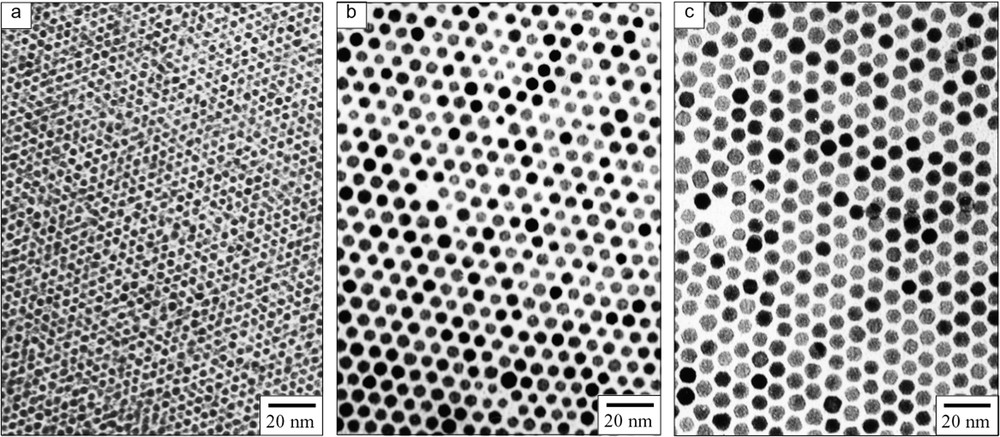
TEM images of DT-Au nanoparticles heat-treated at (a) 150 °C, (b) 190 °C and (c) 230 °C. (From [42], with permission from Wiley-VCH @ 2001.)
2.2 Electron transport property of 2D superlattice of 5.4-nm DT-Au nanoparticles
Recently, the electronic properties of metal nanoparticles have been investigated within the context of decreasing electronic device size features to the nanoscopic level [13]. Applications of individual nanoparticles as computer transistors, electrometers, chemical sensors, and in wireless electronic logic and memory schemes have been described and in some cases demonstrated [53], albeit somewhat crudely at this point. A conventional MOSFET (metal oxide semiconductor field effect transistor), which use ~105 electrons for switching function, will no longer be able to control the flow of electrons as its size reaches the sub-50-nm regime. Thus the ordered metal nanoparticles with well-defined 2D configuration have been focused on to produce the novel nanoelectronic devices like a single electron transistor (SET) which works with one electron at room temperature, allowing the drastic reduction of electric power [1,2,53,54]. The monodisperse metal nanoparticles have potentiality to be the building blocks for nanoelectronic devices using the single electron tunneling effect – the correlated transfer of electrons one-by-one through the object [55].
Gorter and others argued that, provided the energy to charge a metal with a single electron, e/2 C (e is electron charge, C is metal capacitance), was larger than kB T, electrons would be forced to flow through the metal in discrete integer amounts rather than in fluid-like quantities normally associated with transport in macroscopic materials [56]. Further reasoning led to the prediction that current-voltage (I–V) curves of a nanoscopic metal should be distinctly non-ohmic; that is, current steps should appear corresponding to the transport of 1 e–, 2 e–, 3 e–, etc., currents through the metal. In order to avoid thermally induced tunneling processes at room temperature, the metal island of any single-electron device must be less than 10 nm in diameter. This dimension is difficult to reach with electron beam lithography or scanning probe microscopies, although it is now easily achieved by chemists using solution-phase nanoparticle synthesis methods.
Based on this background, we have fabricated the large-scale 2D superlattice of 5.4-nm dodecanethiol-protected Au nanoparticles on air-water interface by the LB method and transferred it onto the 500-nm gap Au electrodes on GaAs [57]. Fig. 4 presents the preliminary I–V curve of this 2D superlattice at 4.2 K. It was found that for large particles of ~5 nm in diameter the electron behavior was dominated by the Coulomb blockade effect at quite low temperature while the I–V response was ohmic at room temperature. To develop the single electron tunneling devices, the Coulomb blockade phenomenon should be observed at room temperature.

Current–voltage curve of 2D superlattices of 5.4-nm DT-Au nanoparticles formed between 500-nm gapped gold electrodes.
2.3 Fabrication of 2D superlattices of small Au nanoparticles
When one uses 2D superlattices of metal nanoparticles as nanoelectronic devices, making use of Coulomb blockade phenomenon at room temperature, metal nanoparticles smaller than 2 nm in diameter are required. Since the formation of ordered structures of such small nanoparticles is difficult mainly due to the weak attractive capillary force between the nanoparticles, one should make use of weak interaction between the protective agents or between the protective agent and the substrate (Fig. 5 ). If these interactions are too strong to be reversible, precipitates of nanoparticles are formed in solution or no rearrangement of metal nanoparticles on substrates occurs, respectively. First research on 2D superlattice formation consisting of metal nanoparticles smaller than 2 nm was reported by Schmid and co-workers early in 2000 [58], where they used an interaction between the protective ligand and the modified substrate to generate 2D superlattices of 1.4-nm Au nanoparticles. The 2D hexagonal and square lattices of Au55 nanoparticles on polymer films were successfully prepared by dipping a poly(ethyleneimine) (PEI)-covered carbon-coated copper grid (for TEM) into an aqueous solution of [Au55(Ph2PC6H4SO3H)12Cl6] nanoparticles. Classical acid-base reactions took place because of the NH functional groups on the PEI. Most of the nanoparticles were found in ordered arrangements of up to a few μm2.
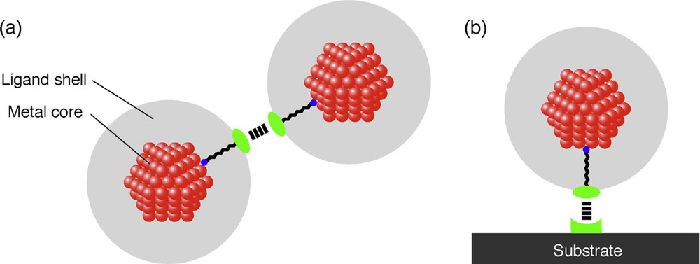
Strategy to fabricate 2D superlattices of metal nanoparticles smaller than 2 nm by using the interaction (a) between the protective ligands and (b) between the protective ligand and the substrate.
Recently, we succeeded in 2D self-assembly of 1.5–1.9 nm Au nanoparticles by using a newly synthesized protective ligand, 2,6-bis(1′-(n-thioalkyl)benzimidazol-2-yl)pyridine (TCnBIP; see inset in Fig. 6a ) [59]. This ligand was designed to have two functional groups, a disulfide group and 2,6-bis-(benzimidazol-2-yl)pyridine (BIP) group, the former serving to produce small Au nanoparticles and the latter inducing the interaction between the ligands. The small Au nanoparticles were prepared by the NaBH4 reduction of HAuCl4

(a) TEM images of 1.9-nm TC8BIP-protected Au nanoparticles (TC8BIP/Au = 1/1 (mol/mol)). The inset stands for the chemical structure of TC8BIP ligand. (b) Schematic illustration of the interpenetration of TC8BIP ligands protecting Au nanoparticles. (c) Perfectly-ordered 2D superlattices of TC8BIP-protected Au nanoparticles on water. ((a) and (b) from [59], with permission from the American Chemical Society @ 2000.)
3 Planar one-dimensional chains of gold nanoparticles
The fabrication of 1D superlattices, or 1D chains, of metal nanoparticles is the most challenging subject when ordering metal nanoparticles, because it is quite difficult to self-assemble metal nanoparticles in low symmetry. If we are able to organize them in 1D configuration, the tunneling behavior between them can be investigated and the nanowiring between the nanodevices, such as single electron transistor and single electron memory, can be realized, which will open the door to generate the future ultra-large scale integrated circuits (ULSI) beyond the ability of the current photolithography technique. In general, the template methods are very effective to order nanoparticles in 1D configuration. For example, one-dimensional chains of gold (Au) nanoparticles have been successfully fabricated by using the pore channels of alumina membranes [63], the step edges of amorphous carbon thin films [64], DNA [65] and biopolymers [66]. However, the formation of long-range 1D chains of metal nanoparticles in planar structure has not been achieved with these template methods.
Recently we have developed a novel method to fabricate a planar array of 1D chains of Au nanoparticles size-controlled by the heat-treatment in the solid state in combination with a specially developed technique to produce nanoscale ridge-and-valley structured substrates using a vacuum process [67]. The 20 nm-thick NaCl overlayers were deposited by thermal evaporation onto the optical grade (110) polished NaCl single crystals (muscut angle < 3°) at 250 °C. Since NaCl(110) is an unstable plane, the film surface becomes faceted with low-energy (100) and (010) planes during the homoepitaxial growth of NaCl. A 30 nm-thick carbon replica layer was deposited directly on the NaCl surface, as shown in Fig. 7 . The carbon layer was floated off from the NaCl substrate in water, and was then loaded on 400-mesh copper grids. As seen in Fig. 7b, presenting an AFM image of carbon replica layer, it preserved ridge-and-valley surface topography with long and straight in-plane macrosteps along [001] of the NaCl epilayer. It was found from the line profile in Fig. 7c that the valley depth and its period are a few nm and ca. 20 nm, respectively. Placing a drop of 3.4-nm DT-Au nanoparticles onto this carbon substrate, followed by the solvent evaporation, led to the fabrication of a planar array of 1D chains of DT-Au nanoparticles, as shown in Fig. 8a . However, almost all the 1D chains were bundles of a few chains. In order to avoid the production of such aggregated structures, the carbon substrate was dipped into DT-Au toluene solution, followed by being withdrawn parallel to the valley direction. As seen in Fig. 8b and c (magnified one), the number of bundles of chains was decreased, and the planar array of 1D chains of Au nanoparticles ordering in a line was formed throughout a few square millimeters of the carbon substrate. The 1D chains formed an array at a distance of ca. 10 nm or ca. 20 nm, which corresponds to a half or one valley period. From AFM measurement of this sample, there is likely to be one line of nanoparticles between two ridges, indicating that the Au nanoparticles were predominantly immobilized in valleys and partly on ridges. The formation mechanism is speculated as follows: When the substrate is withdrawn from the toluene, the Au nanoparticles are adsorbed and assembled mainly in valleys at the upper edge of the substrate by the adhesive [64] and attractive capillary forces [68], respectively. Then the growth of 1D chains of nanoparticles is caused through convective particle flux by solvent evaporation from the already ordered chains [39]. An investigation on the formation of 1D Au nanowire arrays by annealing the planar array of 1D chains is in progress to achieve ohmic nanowiring between the nanoelectronic devices.

(a) Schematic illustration of a preparation of the carbon layer with ridge-and-valley structure and the formation of planar 1D chains of dodecanethiol-protected gold nanoparticles (DT-Au). (b) AFM image of a ridge-and-valley carbon layer on copper grid. (c) A line profile along the white line indicated in (b). (From [67], with permission from the American Chemical Society @ 2002.)
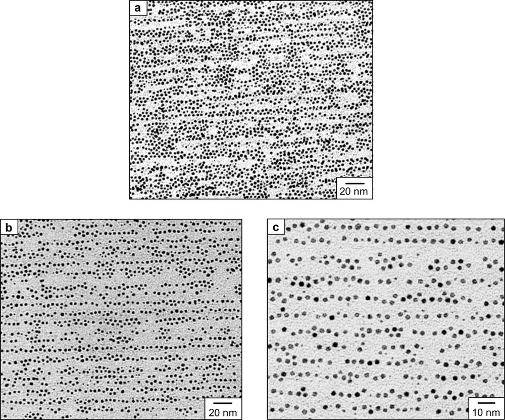
TEM images of 3.4-nm DT-Au nanoparticles on ridge-and-valley carbon layers. (a) Prepared by a drop method. (b) Prepared by a dip method. (c) A magnified image of (b). (From [67], with permission from the American Chemical Society @ 2002.)
4 Conclusions
It is certain that controlling the primary structures of metal nanoparticles, i.e., size, shape, crystal structure, and composition, is still most important, because these structures determine the physical and chemical properties of metal nanoparticles. The current interests of colloid chemists are focused on the fabrication of low-dimensional (1D and 2D) superlattices of metal nanoparticles. Here the fabrication techniques and electron transport properties of 2D superlattices of Au nanoparticles are presented. Now we have a variety of strategies for fabricating the 1D and 2D superlattices, but it is still difficult to produce the desired patterns of nanoparticles at the desired places. The development of methodology to order size- and shape-controlled metal nanoparticles in desired patterns at arbitrary areas will be the key technology for developing the future nanodevices.
Acknowledgements
This work was partly supported by PRESTO, Japan Science and Technology Corporation and a Grant-in-Aid for the Encouragement of Young Scientists (No. 13740392) from the ministry of Education, Culture, Sports, Science and Technology, Japan. I appreciate Prof. M. Haga for his advice on the syntheses of TCnBIP ligands. I thank Dr. Y. Yamamoto for preparing the nano-gap electrodes for I–V measurement of 2D superlattices of Au nanoparticles. My thanks also go to Dr. A. Sugawara for fabricating the ridge-and-valley structured carbon substrates.
Vous devez vous connecter pour continuer.
S'authentifier