

 CC-BY 4.0
1. Introduction
To obtain potential downscaling of active devices such as field-effect transistors (FETs), the emerging of new structures and materials is extremely needed. Nanowire FETs have been reported as promising candidates that makes this miniaturization possible. In one-dimensional devices such as a nanowire, only one of the three Cartesian directions is much larger than the de Broglie wavelength; thus the energy spectrum is analog type in one direction and quantum confined in the other two dimensions. A review on Matt Law [1] of semiconductor nanowires and nanotubes enlighten the electronic and optical properties owing to their unique structural one-dimensionality and possible quantum confinement effects in two dimensions. With a broad draft of compositions and band structures, these one-dimensional semiconductor nanostructures are considered to be the critical components in a wide range of potential nanoscale device applications. One-dimensional semiconducting nanowires [2] and carbon nanotubes [3, 4] are considered an attractive alternative to conventional metal-oxide-semiconductor field-effect transistors (MOSFETs) [5]. One-dimensional nanostructure of carbon nanotube (CNT) provides excellent electronic properties [3, 6] with reduced scattering of charge carriers. Carbon nanotubes [7] and Ge/Si nanowires [8] carrier mean free path characteristics have already studied. Ballistic conduction is achieved in the carbon nanotube FET fabrication [9]. Even if CNTs are used in many applications, the practical difficulties of fabricating the uniform semiconducting nanotubes make the requirement of other one-dimensional nanostructures like nanowires necessary[10]. Nanowires can be fabricated easily due to well-established industrial methodology with high electronic properties and easily combined with the large-scale integrated systems [11]. The advantages and applications of using nanowire transistors in chemical, biochemical, and biosensors [12] making the complete current flow can be blocked if a single analytic molecule interacting with the respective receptor on the nanowire surface was reported [13]. There is more solicitude on the junctionless nanowire transistor and the appropriate doping concentration for the sensor and other applications [14]. The electrical characteristics of the junctionless nanowire transistors are identical to those of regular trigate MOSFETs. Practically, the fabrication of one-dimensional devices needs highly precise nanofabrication units and complex process methods. So, prior to real-time fabrication, a systematic design and simulation is very essential for the cognizant performance of circuit elements and devices. Junctionless nanowire transistors (JNTs) feature bulk conduction as opposed to surface conduction [15, 16, 17], making them an interesting candidate for nanowire (NW) FET biosensor devices with high S/V ratios. One important technological goal aims at the complete integration of a reliable heterogeneous system for which parts can better be fabricated and tested separately and combined possibly as modular components while operating at low powers and ambient conditions. There is tremendous potential for JNT sensors in heterogeneous nanosystems for noninvasive clinical diagnostics, portable, and disposable applications. Junctionless transistors can be used to improve the analog performance of self-cascode configuration. JNT can also be used in digital electronics domain.
In this work, we have designed p-type junctionless nanowire FETs without doping in junctions. To investigate the electrical transfer studies and carrier concentration analysis, various semiconductor materials such as Silicon (Si), Germanium (Ge), Indium Phosphide (InP), Gallium Arsenide (GaAs), and Al(x)Ga(1 − x)As are used. In addition, surface charge and potential analysis are also studied.
2. Materials and methods
2.1. Device design and structure parameters
In this work, the cylindrical structure junctionless nanowire channel is selected. The cylindrical structure is used to make free from edges effect and to improve the short channel effects performance. The cylindrical junctionless nanowire channel is designed with dimensions of 25 nm length and 10 nm diameter and having a p-type doped concentration (NA) of 1 × 1016 cm3. Silicon (Si), Germanium (Ge), Indium Phosphide (InP), Gallium Arsenide (GaAs), and Al(x)Ga(1 − x)As are the materials used in nanowire. This wire is placed on top of a 3 nm thick rectangular Silicon dioxide (SiO2) slab to form the FET element. The gate contact work function is achieved by applying a gate terminal input potential. The SiO2 gate has 4.1 eV work function and relative permittivity value of 4.2. Perfect ohmic contacts were established on both ends of the wire. The theoretical device geometry for simulation is shown in Figure 1. Figure 2 shows the electrical connection of the junctionless nanowire FET. Because of the p-type nanowire FET, the gate signal having the negative bias and drain is also having negative bias with respect to source.
Structure of NWFET device.
Electrical connections of junctionless NanoWire FET.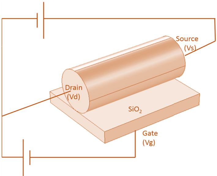
Characteristics of drain current with negative gate voltage.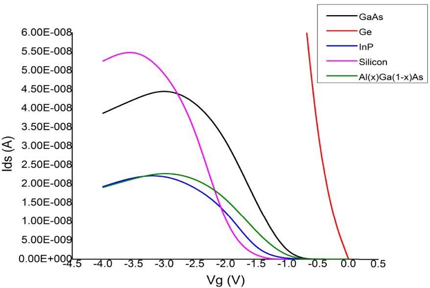
Characteristics of electric potential with negative gate voltage.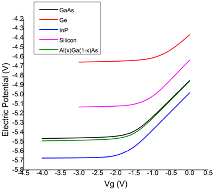
3. Results and discussions
3.1. Effect of gate voltage on drain current
The drain currents were measured by changing the negative gate voltage from zero to 4.0 V. Variations of drain current with biasing the negative gate voltage from 0 to −4 V is shown in Figure 3. The measured values are taken from the center point of the nanowire. The plot indicates that the values of drain current of indirect band gap materials are higher than the direct band gap materials and alloy. From Figure 3, Ge and Si have higher values of drain current compared with other materials. The Al(x)Ga(1 − x)As semiconductor alloy has lower drain current changes. The electron mobility behavior attributes the lower current in InP and higher variations in Ge.
3.2. Effect of gate voltage on electric potential
Figure 4 shows the change of internal electric potential of the nanowire channel corresponding to biasing the negative gate voltage. The semiconductor alloy Al(x)Ga(1 − x)As nearly follow the GaAs because of nearly same band gap value. There is a linear increase of electric potential up to threshold voltage around −1.5 V, after which it saturates. For the same gate voltages, InP nanowires have higher and Ge nanowires have lower electric potential.
3.3. Gate voltage vs. hole current density
Figure 5 shows the relationship between the log of hole current density and the negative gate voltage. As we increased the bias voltage negatively from 0 to −4 V, log of hole current density is provided the relationship of linear changes, which may saturate after the threshold voltage. InP nanowire FET provides higher variations compared to all other materials. Indirect band gap materials have lower hole current density variations when compared to direct band gap materials.
Characteristics of gate voltage vs. hole current density.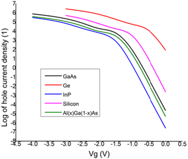
Characteristics of conduction band energy level with the position of GaAs nanowire FET.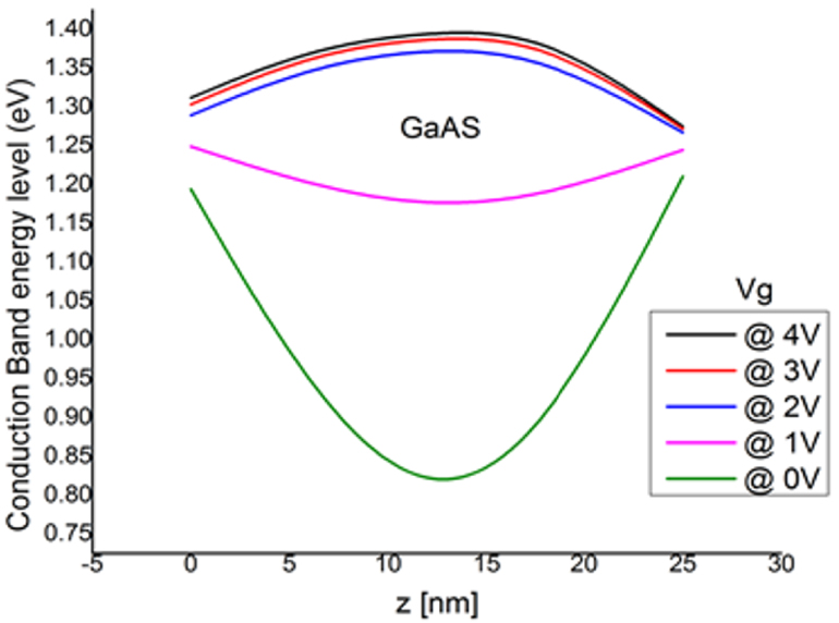
3.4. Conduction band and valance band energy levels
Figure 6 shows the GaAs conduction band energy relationship with the position of the nanowire FET channel. Initially, when applying zero gate potential, both the source and drain ends have the same potential and the middle of the nanowire has very low conduction band energy (0.78 eV). When increasing the negative gate potential, conduction band energy distribution level is increased from 1.25 V to 1.30 V, where the changes will take place. After that it may be conducted. The energy distribution is shown in Figure 6. There is no conduction in 0 V, less conduction in the range 1.25 V to 1.3 V, and more conduction above 1.30 V. The same concept can be applied to valance band energy level also. Figure 7 shows the GaAs valance band energy relationship with the position of the nanowire FET channel. The change of the distribution takes place at −0.20 eV to −0.15 eV and the applied gate voltage is 1 V to 1.5 V.
Characteristics of valance band energy level with the position of GaAs nanowire FET.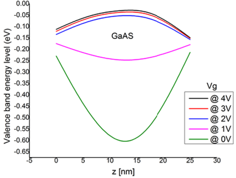
Characteristics of surface charge density with negative gate voltage.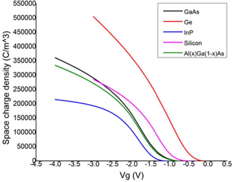
Log of hole concentration @ Vg = −1 V InP nanowire FET.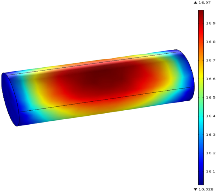
3.5. Surface charge density analysis
Figure 8 shows the dependence of surface charge density with increase in negative gate potential. The differences in the surface charge density are higher in Germanium and lower in InP and others are in between. Figure 8 shows the relationship between surface charge density and negative gate voltage. Change of gate voltage and the variations in charges are displayed clearly in Figure 8.
Log of hole concentration @ Vg = 0 V InP nanowire FET.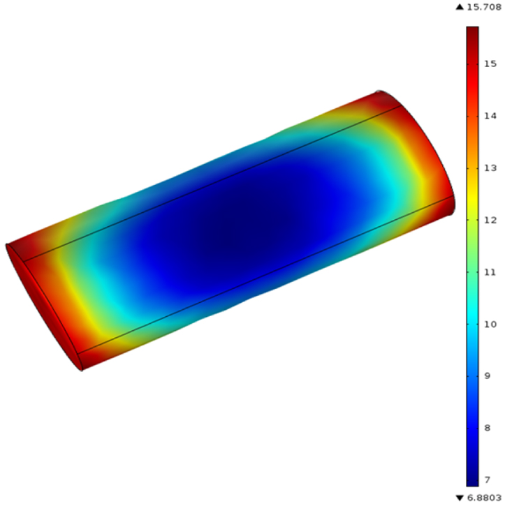
3.6. Hole concentration analysis
The 3D view of hole concentration at the negative bias of gate 1 V and 0 V of InP nanowire FET is shown in Figures 9 and 10. If zero bias is applied to the gate, the concentrations of the holes are very low as shown in blue color and when 1 V bias is applied to the gate, concentrations of holes increased, which is shown red color. It can be understood from the figures that the operation of FET can be achieved with a single type of doping without junctions.
3.7. Surface potential analysis
Figure 11 shows the variations of surface potential relations with negative gate bias and Figures 12 and 13 show the surface potential changes with the change of drain voltage. Changes of surface potential can be directly used in electrochemical sensors. From Figure 11, it is understood that direct band gap materials (InP, GaAs) provide more variations when compared to indirect band gap materials (Ge, Si). From the above results, the InP material provides more variations compared to others.
Characteristics of surface potential with negative gate voltage.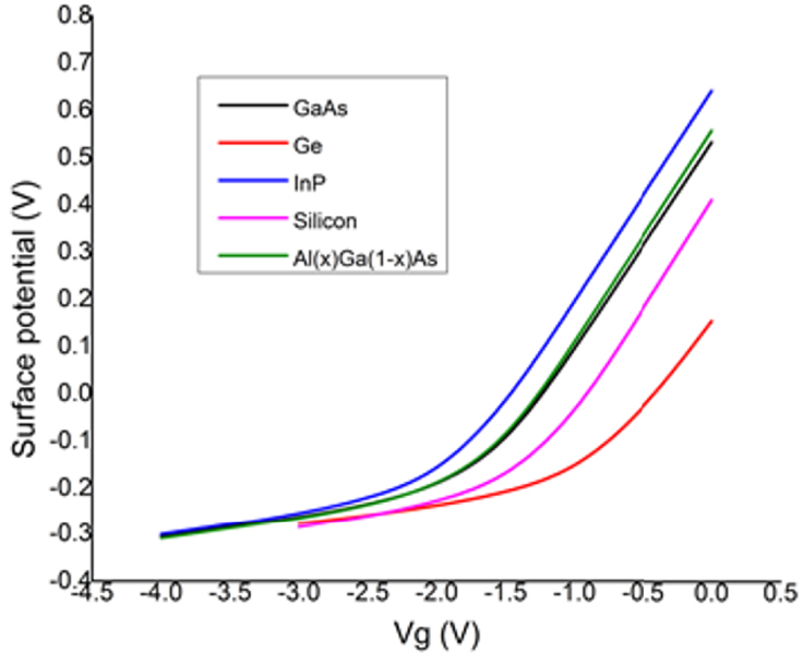
Characteristics of surface potential with negative drain voltage @ Vg = 2 V.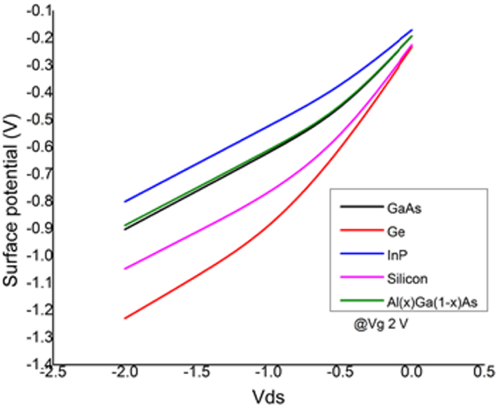
Characteristics of surface potential with negative drain voltage @ Vg = 1 V.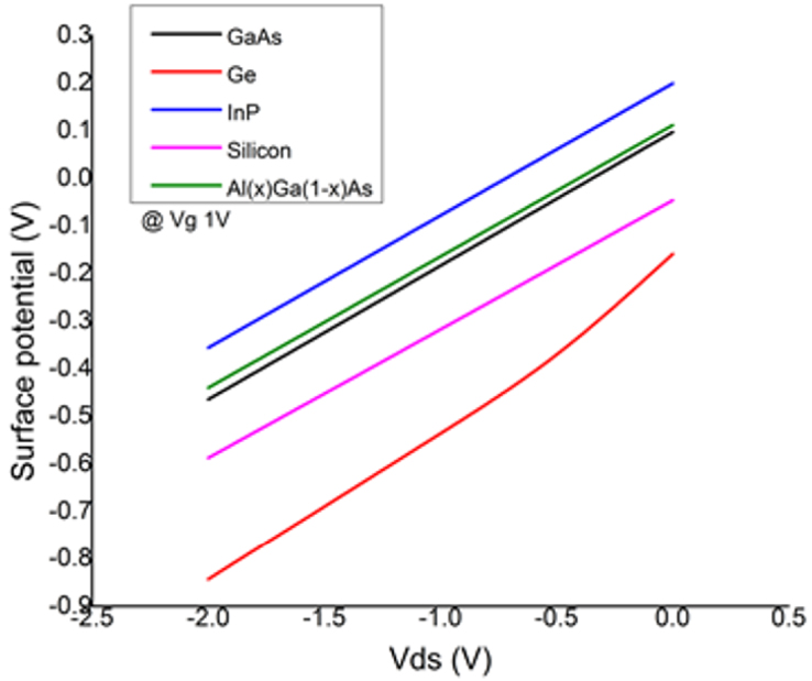
3.8. I–V characteristics analysis
Figures 14–18 show the drain current Id relationship with drain voltage Vd for various channel materials. The change of drain current is shown in the figure for different gate voltages like Vg for −1 V, −1.5 V, and 2 V and for Vg at 2 V. Indirect band gap materials like Germanium nanowire has taken 3.5 μA and Silicon has taken 0.77 μA. The direct band gap materials like GaAs has taken 0.48 μA and InP has taken 0.2 μA. The semiconductor alloy Al(x)Ga(1 − x)As has taken 0.25 μA.
Characteristics of drain current vs. drain voltage for Al(x)Ga(1 − x)As.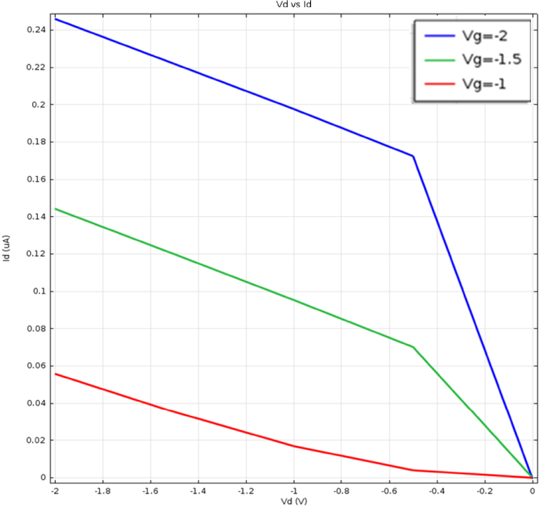
Characteristics of drain current vs. drain voltage for GaAs.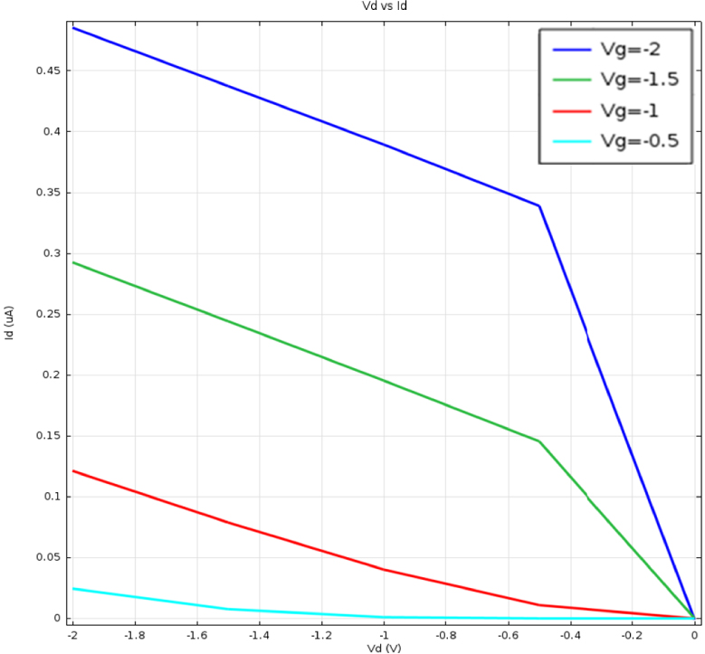
Characteristics of drain current vs. drain voltage for Germanium.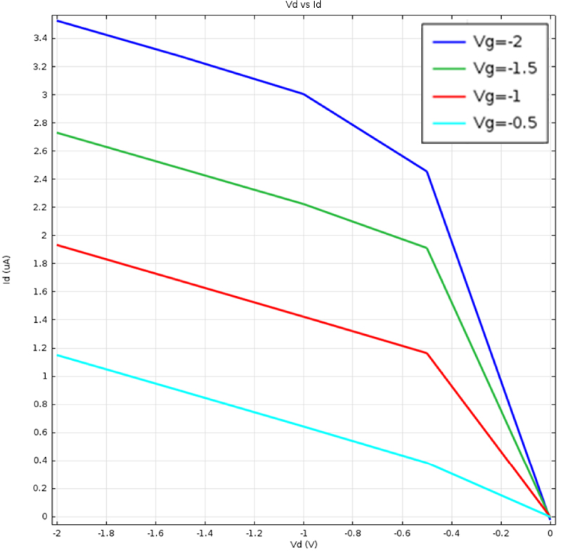
Characteristics of drain current vs. drain voltage for Indium Phosphide.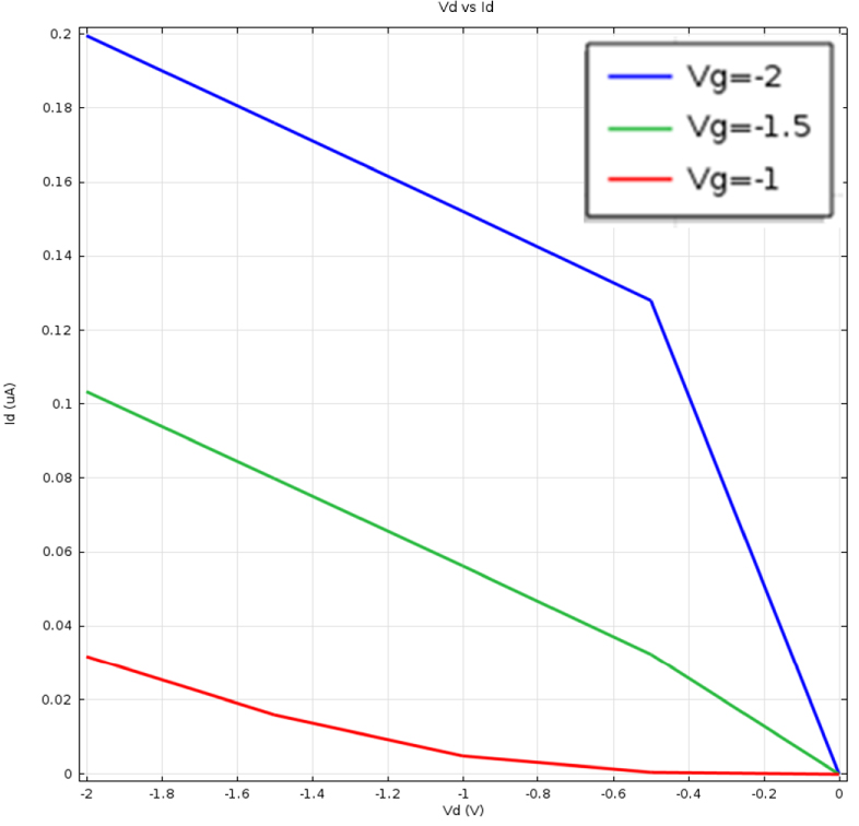
Characteristics of drain current vs. drain voltage for silicon.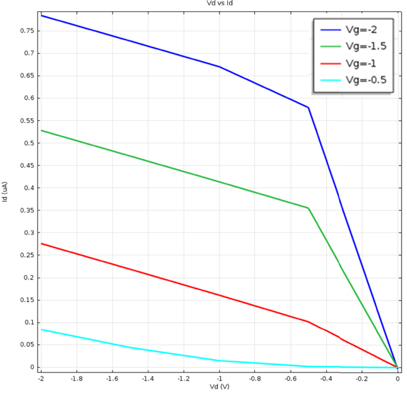
4. Conclusion
The advantage of junctionless nanowire FET is to avoid the difficulty of making junctions and doping in short channel nanowire FETs. In this work, we have successfully modeled and analyzed various p-type junctionless nanowire FETs without doing various doping in junctions. The direct and indirect semiconductor materials and semiconductor alloys (Si, InP, Al(x)Ga(1 − x)As, GaAs, Ge) nanowire FET study has been successfully done. The electrical transfer studies, band gap investigations, carrier concentration analysis, surface charge density, and surface potential studies are carried out. The indirect band gap materials have higher response over the direct band gap material. InP has the highest surface potential values. This high change of surface potential in nanowire FETs can be used in nanostructured sensor applications.