

1 Introduction
Nanoscale materials are the subject of much current interest because they exhibit unique physical and chemical properties that are not available in either isolated molecules or bulk solids. Among these, nanoparticles of II–IV semiconductors prepared as colloids have shown large emission quantum yields, and thus have received considerable attention for optoelectronical applications [1–4]. Potential applications of semiconductor nanoparticles for light generation or luminescent biological labeling have been reported [1–6]. Recent progress of the preparation methods providing high quality nanoparticles with a narrow size distribution allows one to seek to optimize the optical properties fully for specific applications by modifying their surfaces, changing surrounding environments, and making the ordering arrays in two or three dimensions. Optical properties of semiconductor nanoparticles are fairly sensitive to their surface states and surrounding environments, offering a variety of their optical and optoelectronical applications [7–13]. Fundamental understanding of the effects of quantum confinement on the electronic structures is also necessary to optimize the optical properties of semiconductor nanoparticles.
It has been shown recently that the size-selective photoetching technique is very useful for the preparation of semiconductor nanoparticles having the size in the cluster molecular regime [14–16]. The size of the semiconductor nanoparticles can be controlled by changing the wavelength of irradiation light, since the energy gap of semiconductor nanoparticles increases with decreasing particle size. This technique is extremely useful to examine the size dependence of the physicochemical properties, because unexpected changes in surface condition caused by the use of different kinds of chemical species for the preparation can be excluded.
In the present study, we have measured the emission spectra of CdS nanoparticles doped in a poly(methyl methacrylate) (PMMA) film under various experimental conditions. Different size of CdS nanoparticles is prepared by a photoetching technique. It is found that emission of CdS nanoparticles is enhanced with UV irradiation in air and quenched in vacuum. This enhancement and de-enhancement processes are confirmed to be almost completely reversible at least within several cycles.
External electric field effects on optical spectra of CdS nanoparticles have also been examined in order to understand the electronic states as well as the excitation dynamics. The so-called electroemission spectra (plots of the electric-field-induced change in emission intensity as a function of wavelength) have been measured, and the electric field effects on excitation dynamics have been observed.
2 Experimental
Sodium bis(2-ethylhexyl)sulfosuccinate (AOT) and 1,1′-dimethyl-4,4′-bipyridinium dichloride (methyl viologen; MV2+), and stearyl mercaptan (RSH) were purchased from Tokyo Chemical Industry. Cadmium perchlorate was obtained from Kishida Reagents Chemicals. Other chemicals used in this study were supplied from Wako Pure Chemical Industries. Aqueous solutions were prepared just before use with water purified by a Yamato/Millipore WP501 Milli-Q system.
The syntheses of CdS nanoparticles were carried out in AOT-reversed-micelle method as reported previously [17] with a slight modification. A 1.3 cm3 portion of 1.0 mol dm−3 aqueous Cd(ClO4)2 solution or that of 1.0 mol dm−3 aqueous Na2S solution was added separately to 200 cm3 of heptane solution containing 14 g AOT and 5.7 cm3 of water. After being stirred for 1 h, they were mixed together, resulting in the formation of CdS nanoparticles in reversed micelles. To make the particle surfaces cadmium-rich, an additional 0.26 cm3 portion of a 1.0 mol dm−3 aqueous Cd(ClO4)2 solution was added to the solution. The solution was stirred for another 1 h and then the solvent was removed by vacuum evaporation. The obtained yellow solid was dissolved in toluene to give CdS concentration of 3.3 mmol dm−3 (solution A). The surface of CdS nanoparticles was modified by adding RSH (0.26 mmol) to solution A (50 cm3), followed by stirring for 1 h. The solution was refluxed for 2 h and then methanol was added to destroy the reverse micelles, resulting in the precipitation of RSH-modified CdS nanoparticles. The obtained particles were washed with methanol for several times and dissolved in chloroform by sonication. As reported in the previous paper [17], CdS nanoparticles prepared by this procedure had a wide size distribution ranging from 3 to 7 nm with average diameter of 5.0 nm and standard deviation of 0.79 nm.
The size of CdS nanoparticles was controlled by using the size-selective photoetching technique [14–16] to CdS nanoparticles in the reversed micelle solution. An argon ion laser (Ion Laser Technology, model 5500A) was used as a light source of irradiation at 488 and 458 nm. A toluene solution (17 cm3) containing AOT (1.2 g) and 3.0 mmol dm−3 MV2+ aqueous solution (0.5 cm3) was added to solution A (50 cm3). The resulting solution was irradiated under O2 atmosphere with monochromatic light until the absorption spectrum of the solution remained almost unchanged. The photoetched CdS nanoparticles were surface-modified by the addition of 50 mmol RSH. After being stirred overnight, methanol was added to destroy the reverse micelles. The obtained particles were washed with methanol for several times and dissolved in chloroform by sonication. It has been reported in the previous paper [15] that the size of CdS nanoparticles was simply controlled by choosing the wavelength of irradiation light, irrespective of the kind of the stabilizers used in the preparation of CdS nanoparticles. In the present study, therefore, CdS nanoparticles photoetched at 458 or 488 nm were expected to have the size of 2.9 and 3.5 nm, respectively [15].
A certain amount of chloroform solution of a mixture of CdS nanoparticles and PMMA was cast on an ITO coated quartz substrate by a spin coating method. Then, a semitransparent aluminum (Al) film was deposited on the dried polymer film. The ITO and Al films were used as electrodes. The thickness of the polymer film was typically 2.5 μm.
All the measurements were performed at room temperature. Time dependence of the emission spectra during UV photoirradiation was measured using a JASCO FP-777 fluorescence spectrometer with a UV cutoff filter. The scan speed was 500 nm min–1. Continuous irradiation was carried out with a 150-W Xe lamp as a light source in combination with a monochromator and neutral density filters.
Electric-field-induced changes in emission spectra were measured using electric field modulation spectroscopy with the same apparatus as described elsewhere [18–20]. A sinusoidal ac voltage was applied to a sample with a modulation frequency of 40 Hz. Field-induced change in emission intensity was detected with a lock-in amplifier at the second harmonic of the modulation frequency, and the electroemission spectrum was obtained as a function of wavelength. Emission spectra were simultaneously observed by monitoring the dc component of the emission intensity. Hereafter, electroemission spectrum is abbreviated as E–E spectrum, and applied electric field is denoted by F.
3 Results and discussion
Fig. 1 shows the size dependence of the absorption and emission spectra of the CdS nanoparticles doped in a PMMA film at an atmospheric pressure. It is noted that the emission spectra were observed following suitable irradiation by a UV light in air, as will be mentioned later. The absorption spectra exhibit a shoulder roughly at around 450 nm, which is attributed to the transition to the first exciton state. The peak position of the exciton absorption as well as the absorption onset shifts to a longer wavelength with increasing particle size. In all the emission spectra, two emission bands are observed; the narrow emission band close to the exciton absorption and the broad emission band around 500–800 nm. The narrow emission is due to the band-to-band transition from the first exciton state. The broad emission is considered to be emitted from mid-gap states arising from surface defects or un-passivated surface atoms [1,8,11]. Hereafter, the narrow and broad emission bands are called the exciton and trap emission bands, respectively. Note that these two emission bands shift to longer wavelengths, as the particle size increases.
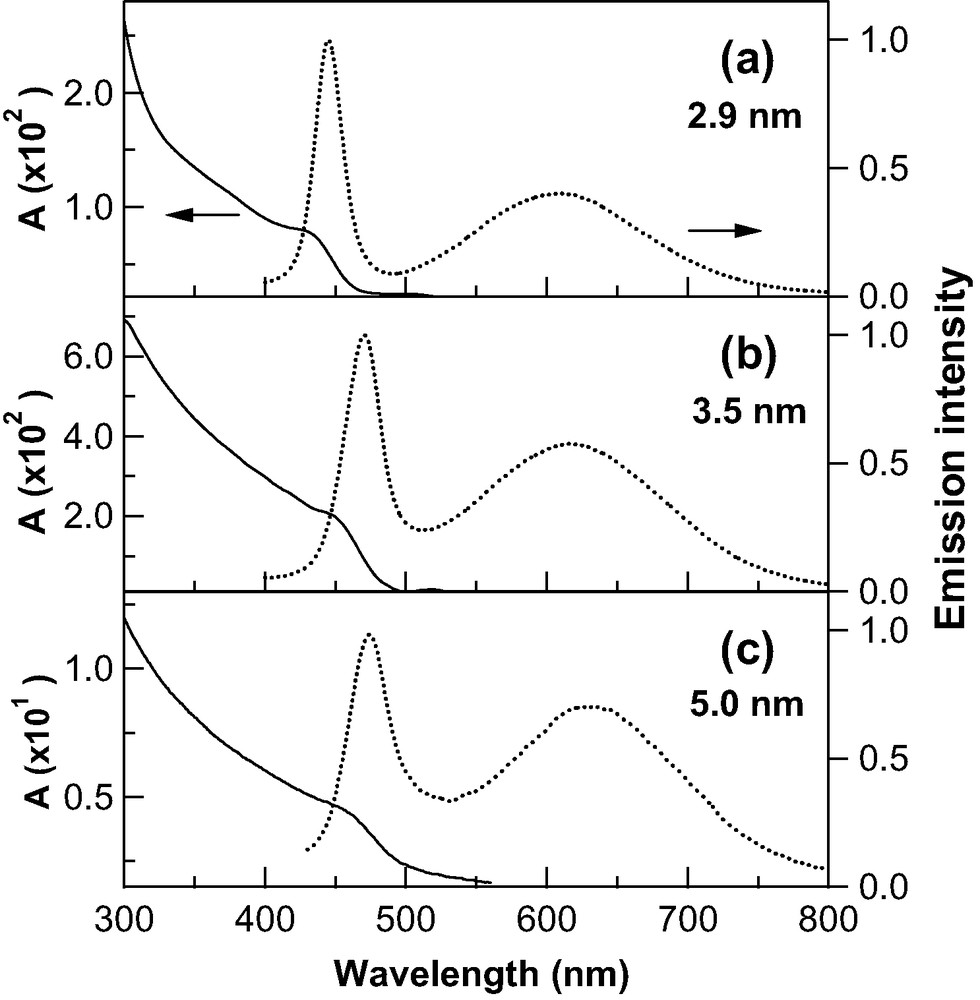
Absorption spectra (solid line) and emission spectra (dotted line) of CdS nanoparticles with an average diameter of 2.9 nm (a), 3.5 nm (b), and 5.0 nm (c) doped in a PMMA film. Excitation wavelength was 340.0 nm.
Fig. 2 shows the emission spectra of the CdS nanoparticles with a size of 2.9 and 3.5 nm doped in a PMMA film as a function of illumination time of 330-nm light in air. Emission spectra of the doped films without UV photoirradiation only show the trap band; the intensity of the exciton band is negligibly small immediately after the sample preparation. Once the doped films are irradiated with 330-nm light in air, a marked increase in exciton emission intensity is observed. The intensity of the trap band also increases with irradiation time, but the magnitude of the increase is much smaller than that of the exciton band. The peak of the trap band also shows a blue shift following photoirradiation. Such intensity changes with 330-nm light irradiation are also observed in the 5.0 nm CdS nanoparticles.

Photoirradiation time dependence of emission spectra of 2.9 nm (a) and 3.5 nm (b) diameter CdS nanoparticles in a PMMA film. A 330-nm light was used for irradiation in air.
Plots of the emission intensity of the 2.9 nm CdS nanoparticles against irradiation time are shown in Fig. 3 both for the exciton emission band and the trap emission band. It is clearly seen that the intensity of the exciton band increases more rapidly than that of the trap band. Note that the radiation density of 330 nm light is the same for both (a) and (b) in Fig. 3. The exciton band reaches to its maximum value and then gradually decreases during photoirradiation, whereas the trap band increases monotonically even after the saturation behavior is observed for the exciton band. Note that the irradiation time with which the maximum intensity of the exciton band is achieved depends slightly on the polymer film treated. 3.5 nm CdS nanoparticles show slight different photoirradiation effect from that of 2.9 nm; both the exciton and trap emission intensities of 3.5 nm particles exhibit a monotonic increase even after the long exposure to the UV light, though the magnitude of the intensity enhancement of the exciton band is larger than that of the trap band.

Plots of intensities of exciton (a) and trap (b) emission bands of 2.9 nm diameter CdS nanoparticles in a PMMA film as a function of irradiation time at an atmospheric pressure.
Fig. 4 shows the plots of the peak positions of the emission bands of the 2.9-nm CdS nanoparticles as a function of irradiation time. Both the exciton band and the trap band show a blue shift by a photoirradiation. The magnitude of the shift is larger in the trap band than in the exciton band. The peak position of the exciton band shifts to 442 nm following photoirradiation and then remains almost constant. A similar temporal behavior is observed in the intensity of the exciton band; the intensity of the exciton band increases monotonically by a photoirradiation and then remains constant (see Fig. 3a). The peak position of the trap band also shows a blue shift by a photoirradiation and then remains constant, but a further irradiation induces a slight red-shift, in contrast with exciton band. Such a time profile is apparently different from that observed in the trap emission intensity; the emission intensity increases only monotonically with irradiation time, as is shown in Fig. 3b. This result suggests that other emitting species appears after 100 min of irradiation, which contributes the increase of the intensity of the trap band.

Plots of peak positions of exciton (a) and trap (b) emission bands of 2.9-nm diameter CdS nanoparticles in a PMMA film as a function of irradiation time at an atmospheric pressure.
Simple exposure to air hardly affects the intensities of the emission bands without UV irradiation. The presence of air, probably oxygen, is absolutely necessary for the above-mentioned change in emission property, as discussed below. Emission spectra of the 2.9 nm CdS nanoparticles observed with and without photoirradiation of 330-nm light in a vacuum condition are shown in Fig. 5a. There is no doubt that emission spectrum is influenced by a photoirradiation only in air, but not in vacuo. When the sample was irradiated in chloroform solution with a 330-nm light over 300 min, the intensity slightly increased (see Fig. 5b), which may be ascribed to a very low concentration of atmospheric constituents in solution. Both results in a polymer film and in solution lead us to a conclusion that both UV irradiation and atmospheric gas are essential for the change in emission intensity of the CdS nanoparticles.
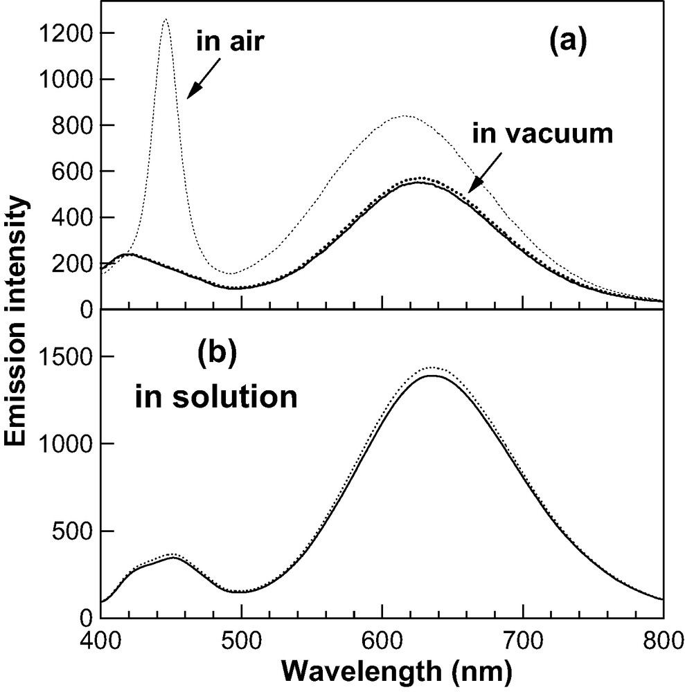
(a) Emission spectra of CdS nanoparticles having a 2.9-nm diameter doped in a PMMA film. Solid and thick-dotted lines show the emission spectra observed at a pressure of 10−5 torr without photoirradiation and with an irradiation of 25 min, respectively. Thin-dotted line shows the emission spectrum observed with a 25-min irradiation in air. (b) Emission spectra of CdS nanoparticles with a 2.9-nm diameter dissolved in chloroform solution saturated with air observed without photoirradiation (solid line) and with an irradiation time of 45 min (dotted line). The diameter of CdS was 2.9 nm, and a 330-nm light was used for photoirradiation.
We have also examined the time dependence of the emission spectra of CdS nanoparticles with a diameter of 2.9 nm in vacuo by employing the sample irradiated by a 330-nm light sufficiently before the measurement. The results are shown in Fig. 6a. At first, the CdS-doped film was irradiated with a 330-nm light in air until the exciton emission intensity reaches to its maximum value. Then the irradiation light was turned off and the sample chamber was evacuated. During the evacuation at a pressure of 10−5 torr, the emission spectra were recorded periodically. As is clearly seen in Fig. 6a, emission intensities of both exciton and trap bands decrease with time in vacuo, and the peak of the bands shows a red-shift. The intensity of the exciton band decreases more rapidly than that of the trap band. Such a de-enhancement of the emission intensity in a vacuum condition occurs with and without irradiation of a UV light. We have also observed the re-enhancement of both emission bands by irradiating the same sample with a 330-nm light in air (see Fig. 6b). This suggests that the alternative change in intensity in air with irradiation of UV light and in vacuo is repeatable, and that the decrease in intensity in vacuo is not due to an irreversible degradation of the nanoparticles.
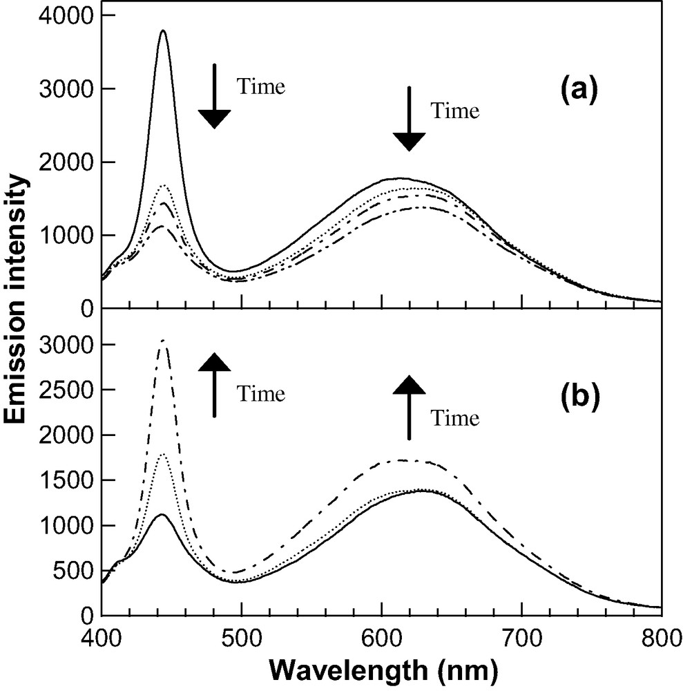
Reversible behavior of enhancement and de-enhancement of emission spectra of CdS nanoparticles with a diameter of 2.9 nm doped in a PMMA film. (a) Emission spectra observed without UV irradiation at a pressure of 10−5 torr as a passage of time. Before the measurements were started, the sample film was irradiated by a 330-nm light in air until the intensity of the exciton band reaches to a maximum value. (b) Emission spectra observed on the way of photoirradiation by a 330-nm light in air. This measurement was carried out following the measurements shown in (a). The spot area of excitation light as well as the sample film treated is the same between the measurements in vacuum (a) and in air (b).
The reversibility of the enhancement and de-enhancement of the intensity is shown in Fig. 7. Emission intensity at the peak is plotted for several cycles of the pressure between 1 atm of air and 10−5 torr. In this experiment, the sample was exposed to air for 30 min with UV irradiation, and then the emission spectrum was recorded. After the completion of the emission measurement in air, the vacuum condition at a pressure of 10−5 torr was held for 45 min and then the emission spectrum in vacuum was recorded. This cycle was repeated for four times to obtain the data shown in Fig. 7. Note that the illumination source was shuttered off during the evacuation of air. Both exciton and trap emission bands increase for each atmospheric-pressure cycle and decrease for each vacuum-pressure cycle. The peak positions of the emission bands also show the same reversible behavior; blue shift and red shift for the atmospheric-pressure cycle and the vacuum-pressure cycle, respectively. The results in Fig. 7 clearly show a photo-switching behavior of the emission property of the CdS nanoparticles in a PMMA film. The enhancement and de-enhancement processes are almost completely reversible at least in several cycles.
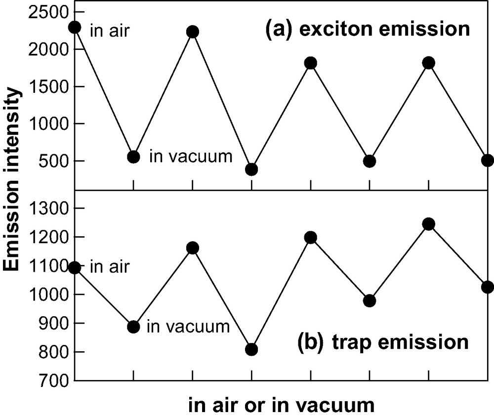
Pressure-cycle dependence of intensities of exciton (a) and trap (b) emission bands of 2.9-nm diameter CdS nanoparticles in a PMMA film. Pressure is cycled between 1 atm of air for 30 min and 10−5 torr for 45 min. The illumination source at 330 nm was shuttered on during the time in air and off during the time in vacuum.
A similar cycle of enhancement and de-enhancement of emission with photoirradiation has also been reported in CdSe quantum dots in a monolayer condition [11]. The emission intensity of the exciton band of the CdSe quantum dots increases by a UV light irradiation in air and decreases in vacuo, as in the case of CdS. However, the trap emission of CdSe nanoparticles in a monolayer film shows the opposite behavior from that of the CdS nanoparticles doped in a PMMA film; the trap emission of CdSe nanoparticles decreases with a UV irradiation in air and increases in vacuo. As a mechanism of photoirradiation effect of CdSe emission, Cordero et al. have proposed the water adsorption model, in which water molecules in air adsorb to the surfaces of the quantum dots upon UV irradiation, and this photo-induced adsorption process is pseudo-reversible. Adsorbed water molecules act to passivate surface traps, which results in the increase in emission intensity [11]. In this model, however, the role of the UV photons for the adsorption process seems to be unclear, since capping materials as well as water molecules do not absorb UV photons around 330 nm. In the present system, a complex formation between CdS nanoparticles and oxygen molecules upon UV irradiation seems to play a significant role. The surface states may be passivated by the complex formation. In order to examine whether or not water molecules also play a significant role in the present system, further experiments are necessary.
We have also examined external electric field effects on emission properties of the CdS nanoparticles in a PMMA film. Fig. 8 shows the E–E spectra of 2.9-nm CdS nanoparticles doped in a PMMA film, together with the emission spectra simultaneously observed. Excitation wavelength was 330.0 nm, where the field-induced change in absorption intensity is negligibly small. The magnitude of the field-induced change in emission intensity was confirmed to be proportional to the square of applied field strength. In the measurements of the E–E spectra, we first measured the E–E spectrum of the sample without UV irradiation at a pressure of 10−5 torr, which is shown in Fig. 8a. Then the sample was irradiated by a 330-nm light in air for 180 min and the E–E spectrum was measured, which is shown in Fig. 8b. The sample was further irradiated by a 330-nm light for 660 min in air and the E–E spectrum was again measured, which is shown in Fig. 8c. Note that the exciton emission intensity decreases after 250 min of irradiation (see Fig. 3a).
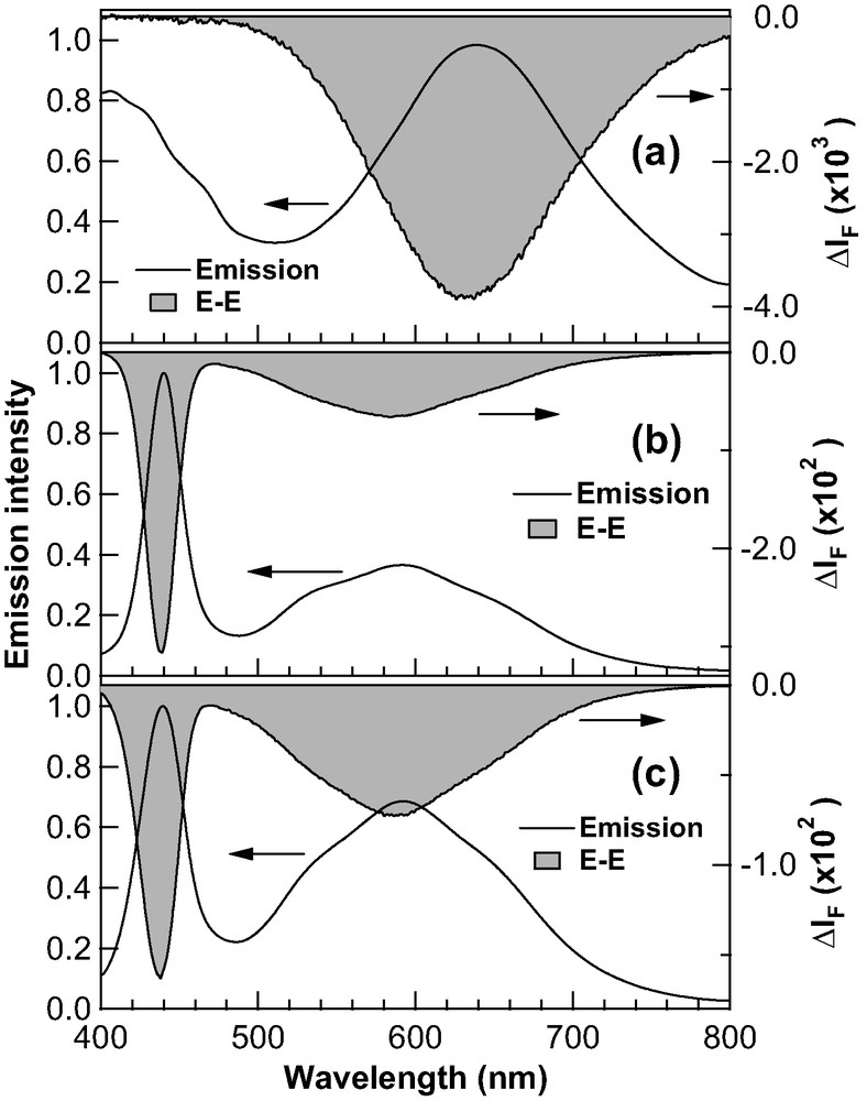
E–E spectra (shaded line) of 2.9-nm diameter CdS nanoparticles in a PMMA film, together with the emission spectra simultaneously observed (solid line). The E–E spectrum in (a) was observed at a pressure of 10−5 torr without irradiation of 330-nm light before the measurement. The E–E spectra in (b) and (c) were observed in air following 180- and 660-min photoirradiation by a 330-nm light, respectively, in air. The broad signal observed in the emission spectrum of (a) around 420 nm is an artifact of the instrument. Excitation wavelength was 330.0 nm. Applied field strength was 0.5 MV cm−1.
Both exciton and trap emissions are quenched by F, as shown in Fig. 8. The E–E spectra of the CdS nanoparticles with a 3.5- or 5.0-nm average diameter also show the same behavior; both emissions are quenched by F. We can, therefore, conclude that the emission quantum yields both of the exciton emission and of the trap emission of the CdS nanoparticles in a film are de-enhanced by F. The magnitude of the field-induced decrease in emission intensity is summarized in Table 1. As already mentioned, the exciton emission intensity reaches to a maximum with an irradiation time of ~250 min in air. With this irradiation time, the magnitude of the field-induced decrease in intensity also shows a maximum not only for the exciton band but also for the trap band under the present experimental conditions. As shown in Fig. 3b, the trap band intensity monotonically increases even after an irradiation time of 250 min. These results suggest that several species, which show a similar emission spectrum in the 500–800-nm region but show a different field dependence of quantum yield from each other, co-exist in a doped polymer film following a long exposure to a UV light. Note that the exciton band is not observed in the E–E spectrum in vacuo because of the negligible intensity of this band in vacuo (see Fig. 8a).
The magnitude of the field-induced quenching of emission of CdS nanoparticles with an average diameter of 2.9 nm in various conditionsa,b
| In vacuo | In air | In air | |
| No irradiation | 180 min irradiation | 660 min irradiation | |
| Trap | 0.43 | 2.20 | 1.00 |
| Exciton | 2.90 | 1.20 |
a In units of percentage.
b Applied electric field was 0.5 MV cm−1.
The transition dipole moment of CdS nanoparticles is known to be hardly affected by F, based on the electroabsorption measurements in a PMMA film [21]. Then, the field-induced quenching of emission observed in the present experiments suggests that the rates of non-radiative processes from the emission states are accelerated by F. From the measurements of the electroabsorption spectra of semiconductor nanoparticles, Alivisatos et al. have suggested that the first exciton state of the semiconductor nanoparticles with a diameter larger than 2.5 nm has large charge transfer (CT) character arising from an asymmetric charge distribution in the excited state [22]. It has been shown that the rate of CT process is notably influenced by F in mixtures of donor and acceptor molecules which show photoinduced electron transfer [18–20]. Then, the observed field-induced decrease in exciton emission intensity can be attributable to the field-induced enhancement of the rate of the non-radiative process from the first exciton state to the ground state, which may be regarded as a kind of back electron transfer. It is not confirmed whether the field-induced decrease in emission intensity of the trap band is ascribed to a change in rate of the non-radiative process from the trap state or a change in rate of the formation of the trap state. Direct measurements of the field-induced change in emission decay profile will be very helpful to elucidate the origin of the field-induced change in trap emission intensity [23].
In conclusion, we have shown that emission behavior of the CdS nanoparticles doped in a PMMA film can be controlled by a combination of a UV light irradiation with an air. With a UV light irradiation in air, the exciton emission intensity increases markedly, being accompanied by a blue shift of the emission spectra. The trap emission intensity also increases with irradiation time, but the magnitude of the change is smaller than that observed in the exciton band. Both exciton and trap emission intensities which are enhanced by a photoirradiation in air are strongly de-enhanced by evacuating the sample cell to a vacuum; i.e. a pressure of 10−5 torr. Atmospheric gas as well as UV irradiation is essential for causing such an enhancement and de-enhancement process, which is almost completely reversible at least in several cycles. Application of an external electric field also induces a quenching in emission intensity. The field-induced de-enhancement of the exciton emission intensity suggests that the exciton state has a CT character and that the non-radiative decay rate from this state is accelerated by applying an external electric field.
Acknowledgements
This work has been supported in part by Grants-in-Aid for Scientific Research (Grant Nos. 15205001, 15655001, and 15685005) and for Scientific Research on Priority Area (417) from the Ministry of Education, Culture, Sports, Science, and Technology in Japan.