

1 Introduction
All-solid-state nanostructured solar cells consist of a nanoporous interpenetrating network of an n-type (e.g., TiO2) and a p-type (semi)conductor (e.g., CdTe, CuInS2, dye) [1–5]. They were proposed as an alternative to the more classic dye sensitized solar cells, where a dye-coated porous TiO2 is immersed in a redox electrolyte [6]. Dry, all-solid-state nanostructured cells have projected advantages for cell and module manufacturability and stability, but presently perform less than wet cells. There are some indications in literature to explain this [7], but nevertheless there is common agreement that presently there is still a lack of basic understanding, which is hindering further development of these cells. The complicated 3-dimensional geometry of nanostructured cells is unmanageable with standard modeling. In this paper, two methods are compared to model the I–V curves of nanostructured solar cells. The aim is to gain insight in the working mechanisms of these cells.
In this work, it is shown that the NM and the EMM can describe the same physical structure, when they are set up properly. They both implement the ‘semiconductor equations’ (Poisson; drift, diffusion; generation, recombination; continuity). When ideal Shockley diodes are used in the NM, some physical recombination mechanisms are described correctly, but other mechanisms are not. More elaborate diode laws however can represent other, specific recombination mechanisms. While for each NM an equivalent EMM can be set up and vice versa, a NM is generally more intuitive, but it requires great care to relate the NM parameters to a particular physical situation. On the other hand, the combination of the EMM and a solar cell device simulator is easy to use, but it requires some parameters, most of them unknown.
2 Models
2.1 The network model
In the network model (NM) [8,9], we decouple the effects at microscopic (nm) and macroscopic (μm) scale.
At a microscopic scale, the complicated 3-dimensional nanoporous geometry of two interpenetrating networks is simplified to a quasi-periodical nanoscale ordering of an n- and a p-type (semi)conductor, forming a ‘unit cell’. It has been recognized before that nanoscale unit cells are almost field free. The periodical boundary conditions in a nanoscale periodic structure even lower the field for the same unit cell size [8,9]. It is called a ‘flat-band cell’: the total band bending can be totally neglected; the conduction and valence band are flat, as well as both Fermi levels (or electrochemical potentials) EFn and EFp. A possible discontinuity in electron affinity Δχ imposes the conduction band cliff. Fig. 1 shows such a unit cell for a periodic structure of equally thick layers of TiO2 and CdTe. For our simulations, we take Δχ = χTiO2 – χCdTe = 0.4 eV. Values of Δχ up to 0.7 eV were reported [10]. The separation between the Fermi-levels equals the ‘applied voltage’ over the cell.
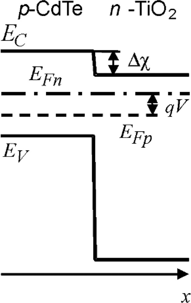
Flat-band approximation of a nanoscale unit cell in a periodic structure of TiO2 and CdTe.
At a macroscopic scale, we simplify the two interpenetrating networks to an electrical network. In a real solid-state nanostructured solar cell, a 3-dimensional n-type network makes electrical contact with one electrode. The p-type network forms a complementary network which makes contact to the opposite electrode. To keep the model manageable, both networks are simplified to one dimension. We obtain the network shown in Fig. 2. Each diode in the row stands for a periodic, flat-band unit cell as just described. The resistors stand for the percolation in the p-network (top), and in the n-network (bottom). Two contact diodes describe possible Schottky barriers at the electrodes.
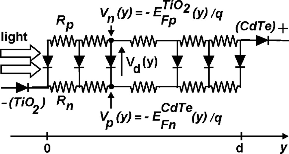
A one-dimensional network connection of the unit cells, represented by the diodes, used to simulate the macroscopic cell. The resistors stand for the percolation of the p-network (top), and the n-network (bottom). Two contact diodes describe possible Schottky barriers at the electrodes.
In this way, with the NM, we have created a physical model for a small nanoscale ‘unit cell’ and a phenomenological network model for the geometry of the complicated 3-dimensional nanoporous structure.
The voltages of the network nodes represent the local Fermi levels (or electrochemical potentials) in the physical situation. More precisely, the voltage of the nodes in the n-branch equals , and the voltage of the nodes in the p-branch equals . The minus signs and the factor 1/q are because EF represents an electron energy, not an electrical potential.
Constant resistors stand for transport by drift and diffusion, since a voltage drop Vn(y1) – Vn(y2) in the network stands for a Fermi-level gradient in the physical situation. Transport by space-charge limited currents would require adjustment of the I–V laws for the resistors, i.e. I ÷ V2/d3, where d is the length of a resistor.
The local voltage difference Vd(y) over a network diode at position y is given by:
| (1) |
In the network description, all other physical quantities such as electrostatic potential ϕ, electron and hole concentration n and p within the unit cells and hole and electron current density are lost and lumped in the current–voltage law of the diodes and the resistors.
When ideal Shockley diodes are used in the NM, the diode current under illumination is given by:
| (2) |
| (3) |
Shockley–Read–Hall recombination (recombination via trap centers) is given by:
| (4) |
2.2 The effective medium model
In the effective medium model (EMM), which has been proposed in literature (e.g., [11]), the whole p–n nanostructure is represented by one single effective medium semiconductor layer. We consider selective contacts, i.e. one contact only accepts electrons, the other one only accepts holes. This creates the driving force for the separation of generated electron-hole pairs. The effective medium is characterized by an ‘averaging’ of the properties of the n- (e.g. TiO2) and the p-material (e.g., CdTe). The effective medium has one conduction band namely the conduction band of the n-type material or the lowest unoccupied molecular orbital (LUMO) of the acceptor molecule in a bulk heterojunction solar cell. The effective medium has also one valence band namely the valence band of the p-type material or the highest occupied molecular orbital (HOMO) of the donor molecule in a bulk heterojunction solar cell. This configuration is then fed into a standard solar cell device simulator, e.g., SCAPS [12]. Also other carrier related properties of the effective medium semiconductor are given by the corresponding material: the mobility μn, the diffusion constant Dn and the effective density of states NC of the conduction band are those of the n-material, whilst the values of μp, Dp and NV are those of the p-material. Non-carrier related properties, such as the dielectric constant ɛ, the refractive index n, and the absorption constant α are influenced by both materials. The precise way in which this happens depends strongly on the details and the size scale of the intermixing. For particles smaller than the wavelength of the illumination, a true effective medium theory can be used [13].
For our simulations with SCAPS, we choose a cell thickness of d = 10 μm of an almost intrinsic material (doping density of NA = ND = 104 per cm3). As bandgap of the effective medium, we take . The effective medium is further characterized by a relative dielectric constant of ɛ = 30 and an electron affinity of χ = 4.7 eV. To introduce Shockley–Read–Hall recombination in the bulk, we add a single neutral defect level at 0.05 eV above the valence band. The barrier ϕb of both contacts is 0.2 eV. The built-in potential Vbi is then . We illuminate the cell from the electron selective contact (n-contact side).
3 Equivalence of both models
3.1 Comparison
The question to be answered is how the NM and the EMM are related: do they describe the same cells and the same phenomena?
Both models implement the ‘semiconductor equations’ (Poisson; drift, diffusion; generation, recombination; continuity). In the NM, the values of the network resistances Rn and Rp must be chosen so that the Poisson equation and the current equations are satisfied; the continuity equations describing generation and recombination are comprised in the current–voltage law of the diode. The ‘semiconductor equations’ are automatically guaranteed when an effective medium configuration is implemented in a solar device simulation program.
In general, the NM is a more intuitive model which can be treated by electrical network programs e.g. OrCAD PSPICE [14]. Interpretation of network properties (voltage and current at the nodes) though, can only partly be given in terms of physical quantities like Fermi-levels; the electrostatic potential ϕ and the electron and hole concentration n and p within the unit cells are lost, and lumped in the current–voltage law of the diode. One has to pay attention to correctly relate the NM parameters to a particular physical situation.
The EMM treated with a solar cell simulation program (e.g. SCAPS) is easy to use, but it requires some parameters, most of them unknown. Although the interpretation afterwards can be simpler than in the NM, the problem is to define the properties of the effective medium properly so that it describes the physical structure correctly. Less physical parameters are lost in this model than in the NM, but great care must be taken into account when relating a physical parameter of the effective medium to a physical parameter of the real nanostructured solar cell.
Some problems are more easily tackled by the NM than by the EMM and vice versa. In the NM, network programs can easily simulate transient measurements after switching to a new condition (at present, simulation of transient phenomena is usually not included in standard solar cell simulators [15]). On the other hand, solar cell simulation programs used in the EMM are able to simulate more complicated recombination mechanisms than the ones represented in the NM.
The NM and the EMM are able to describe the same physical structure when they are set up properly. The models are equivalent, but one has to pay attention that both methods really correspond. The diode light current JL(y) in the NM can be interpreted as the carrier generation in a specific part of the effective medium. In both models, the generation depends of the position y by the absorption law as exp(–αy). The diode dark current JS(y) in the NM corresponds with the carrier recombination at a position y in the EMM. In the one-dimensional NM, the resistance Rn(y) (in Ωcm) can be linked to the electron mobility μn via the resistivity ρn (y) = [q μn n(y)]−1 (and the same for Rp(y)).
As an illustration, we studied the influence of the mobility on the efficiency of a solar cell with both the NM and the EMM, and compared the results.
3.2 Results of simulations
In our previous articles [8,9], it was shown that in a simplified NM, i.e. constant resistances Rp and Rn, the solar cell performance is tolerant to Rn upon illumination on the n-side. This resistance Rn of the n-type network can even be beneficial to the open circuit voltage Voc and to the solar cell efficiency if the absorption α is high enough. On the other hand, even a small resistance Rp of the p-type network deteriorates the cell efficiency rapidly. This can be understood as follows: the cells are illuminated from one side, which implies that the unit cells generate less current and voltage as the light penetrates in the cell. Ideally, all generated currents are added to obtain the total light current. The open circuit voltages however are not summed, they are rather averaged. This is an essential difference with classical solar cells. Under illumination, the unit cells at the illuminated side are below their own local Voc(y) because all cells in the stack of Fig. 2 are forced to be at the same voltage. For the same reason, the cells in the bulk and at the rear end of the stack are above their local Voc(y). In Fig. 3, we see that a non-zero resistance in the n-sub-network improves the cell efficiency η if the resistance is not too high. This is because cells deep in the stack, adversely contributing to Voc, are effectively decoupled by a larger Rn. The voltage Vd(y) over the elementary cells is now non-uniform, the cells at the illuminated side carrying a larger Vd(y). This is favorable for the open circuit voltage of the whole cell, which equals Voc = Vd(0) when Rp = 0 Ω (see Fig. 2); the cells at the front are able to carry their generated hole current with no losses to the rear contact. This is also the reason why resistance in the p-sub-network is detrimental: it decouples the most illuminated cells at the front from the rear contact. Fig. 3 shows that a value of Rn·A = 150 Ω cm2 is beneficial and Rn·A = 500 Ω cm2 can be tolerated, whereas a value of Rp·A exceeding 1 Ω cm2 is detrimental.
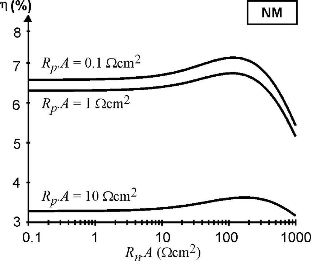
Solar cell efficiency η as a function of the resistance Rn·A in the n-sub-network calculated with the NM. The parameter is the resistance Rp·A in the p-sub-network. Calculated with α = 105 cm−1. Note the sensitivity of η to Rp·A.
The question arises if the EMM gives similar results. Therefore, simulations with SCAPS were done with the set up described above in 2.2. Again, the cell is illuminated from the n-side (the electron selective contact). Instead of the resistance of the NM, the parameter in the simulations of the EMM is the mobility μ of the carriers. Simulations were done with the electron and hole mobilities varying from 10−4 to 102 cm2 V–1 s–1.
The results in Fig. 4 show that for the EMM the relative efficiency η only deteriorates for low electron mobilities μn and that a low hole mobility μp is very detrimental (corresponding with high resistances R in the NM). Notice the similarity with Fig. 3 of the NM. It is remarkable that both results correspond, because the NM was calculated for constant values of Rn and Rp, whilst in the EMM the resistivity and the mobility can vary over up to seven orders of magnitude.

Relative solar cell efficiency η as a function of the inverse electron mobility 1/μn calculated with the EMM. The parameter is the hole mobility μp. Calculated with α = 105 cm−1. Note the similarity with Fig. 3 of the NM.
More detailed studies show that, if the absorption is high enough, the cell efficiency even rises for low electron mobilities thanks to an improved open circuit voltage Voc; the cell efficiency does not suffer from a lower electron mobility μn unless it is below 10−3 and 10−4 cm2 V–1 s–1, depending on the absorption α. This result is similar to the NM where a rise in the resistance Rn of the n-network also improved cell efficiency thanks to a better Voc.
Simulations with the hole mobility μp as parameter show that the short current density Jsc quickly drops when the hole mobility is lower than approximately 1 and 0.1 cm2 V–1 s–1. This is the reason for the deterioration of the cell when the hole mobility is too low. Again, this result is similar to the NM where a small resistance Rp of the p-network drops the cell efficiency rapidly.
The tolerance towards the n-network and the intolerance towards the p-network could be an explanation for the substantially poorer behavior of ‘dry’ or all solid-state cells compared to ‘wet’ or dye sensitized solar cells [7]: the ion conduction in the electrolyte is better than the hole conduction in the ETA absorber or the solid-state p-conductor, and this is crucial for the cell performance, as we showed. Resistance in the n-network is not crucial, it is even beneficial if not too large.
Because both models are symmetrically set up, the role of the p and n sub-network will be interchanged when we illuminate the cell from the p-contact side; simulations confirm this.
Further calculations were carried out to quantify the efficiency enhancement Δη resulting from the beneficial effect of resistance in the n-network. For the parameters used, the optical absorption α should exceed 3 × 104 cm−1 in the NM and 105 cm−1 in the EMM to see any positive Δη at all. The effect is modest, e.g. 0.7% absolute efficiency (or a rise of 10% relative) for a high value α = 105 cm−1, a moderate value Rn·A = 150 Ωcm2 and a resistanceless p-sub-network (Rp·A = 0 Ωcm2) in the NM. In the EMM, an absorption coefficient of even 2 × 106 cm−1 is needed to increase the efficiency (a rise of 10% relative). However, the mere fact that a moderately poor conduction in the n-network does not completely destroy the cell performance, is a remarkable result in itself.
It is also clear that the cell efficiency can not be high if not enough photons are absorbed to create electron-hole pairs. As well as in the NM as in the EMM, the cell efficiency drops quickly if the absorption lowers from 5 × 103 cm−1.
4 Conclusions
We have suggested two methods to model the I–V curves of nanostructured solar cells: the NM in which the solar cell is represented by resistors and diodes, and the EMM in which the whole p–n nanostructure is represented by one single effective semiconductor layer, which then is fed into a standard solar cell device simulator. These models were compared and it was shown for example that in both models the structure, when illuminating the n-side, is tolerant to resistance in the n-network but not to resistance in the p-network. This could be an explanation for the substantially poorer behavior of ‘dry’ or all solid-state cells compared to ‘wet’ or dye-sensitized solar cells.
Acknowledgements
The European RTN ‘ETA’ (HRPN-CT2000-0141) (C.G.). The Research Fund of the University of Ghent (BOF–GOA) (M.B.). The IWT SBO-project 030220 NANOSOLAR funded by the Institute for the Promotion of Innovation by Science and Technology in Flanders (IWT).