

1 Introduction
The ability of certain molecules to level out uneven topographies during metal electrodeposition has been known for some time [1–3]. A classic example is the molecule coumarin during the electrodeposition of Ni [4–6]. Interest in leveling agents for Cu was renewed once Cu electrodeposition became a widely adopted manufacturing process for on-chip Cu interconnects [7]. In damascene Cu integration, electrodeposited Cu must be planarized by polishing down to the dielectric material to reveal the in-laid Cu wires. This planarization process is known as chemical mechanical polishing (CMP). As one might expect, the polishing process tends to proceed with less complication if the electrodeposited Cu surface topography is not excessive; leveling agents for electrodeposited Cu thus find use for this purpose. Although some processes for reducing as-plated Cu topography without the use of such leveling agents have been demonstrated [8], it is still common today for chip manufacturers to rely on such molecules in their Cu plating chemistries to minimize Cu topography. As the Cu electrodeposition and planarization steps must be repeated several times to build up the multiple levels of Cu wiring used in current logic chips, it is important that these two processes are well-integrated for manufacturability. In this study, we experimentally characterize the impact of leveling additives used in electrodeposition on the subsequent Cu planarization process for the wafer and pattern-scales.
2 Experimental
Wafers for all experiments were fabricated at the Albany Nanotech center in Albany, NY, using single level damascene-patterned 300 mm silicon wafers. Electrodeposition was carried out using a commercially available, standard 300 mm Cu plating tool and a typical acid-sulfate based Cu plating chemistry that finds use in the industry. Electrodeposition for damascene Cu interconnects has been in manufacturing use for some time and is considered a well-established process; descriptions of the approach as well as models explaining the bottom-up fill process are available in the literature [7,9–11]. Damascene Cu plating chemistries of the same type used in this study have been discussed in some detail in the literature over the past several years [12–21]. Most additives used in these chemistries are commercially available from both specialized industrial vendors and general chemical reagent suppliers (e.g. poly [ethylene glycol] or “PEG”, bis[3-sulfopropyl]) disulfide or “SPS”, and polyvinylpyrrolidone or “PVP” for suppressor, accelerator, and leveler, respectively). CMP of the electrodeposited Cu on the Si substrates also took place using a commercially available, standard 300 mm Cu polish tool with Cu and barrier slurries typical of those industrially used. Details of 300 mm Cu electrodeposition and CMP tooling and processing are beyond the scope of this study and described elsewhere [22–24]. The leveling molecule concentration was varied in some cases between “1x” and fractions thereof; “1x” indicates a concentration that could be considered nominal for this chemistry. In some cases, topography of the wafers was measured by profilometry using a KLA-Tencor profilometer.
3 Results and discussion
Fig. 1 shows the as-plated topographies for various leveler concentrations measured by profilometry. The macro of interest being profiled has a row of six areas each with a repeating pattern for various line-space combinations. As each patterned area is approximately 200 microns on a side, it is much larger in size than the line-space distance for most of the line-space combinations. The nominal thickness of the plated Cu is 150 nm, a little more than the patterned feature depth. A couple of typical features of the pattern-scale behaviour are evident here. First, wide lines or pads tend to fill up slowly, resulting in a locally lower Cu deposit thickness, sometimes referred to as “underfill”, while for narrow lines, a locally high thickness or “mounding” tends to result. An example of this linewidth effect is seen for lines 0.1 μm in width spaced 0.2 μm apart that exhibit mounding compared to the area having 0.8 μm wide lines with the same 0.2 μm spacing. A more exaggerated example of the linewidth effect is the area with 50 nm line 50 nm spacing where the highest degree of mounding is observed. The preceding observations are all consistent with models in the literature discussing a locally high concentration of an accelerating additive at the bottom of narrow features that leads to a rapid bottom-up filling of the feature [10,11]; it should be expected that densely patterned areas of narrow features will have locally high concentrations of the accelerating additive once the features are filled, resulting in a locally thicker Cu deposit. Finally, the presence of the leveling additive clearly lessens the degree of Cu topography, especially at its nominal concentration. It is effective for reducing mounding over dense patterns, but appears significantly less so for improving underfilled areas at this electrodeposited Cu thickness. The mounding effect is clear in Fig. 2, a scanning electron microscope (SEM) image showing a cross section of the 50–50 nm line-space area for wafers processed with and without the leveling molecule (otherwise the electrolyte chemistries were identical). The nominal plated Cu thickness in this section is 150 nm, but the onset of mounding is already clear over the dense lines for the leveler-free chemistry.
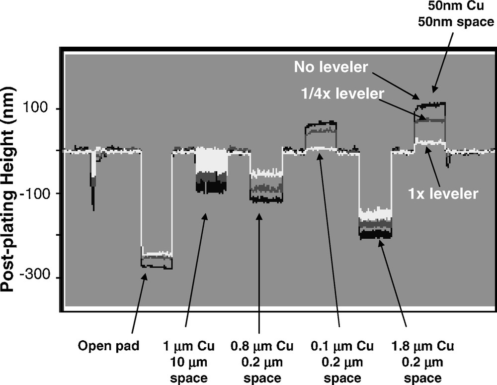
Profilometry scan over arrays of various line spacing combinations as indicated. Nominal electrodeposited Cu thickness is 150 nm. Cu electrodeposited with a leveling additive has much less mounding of dense arrays of narrow Cu lines compared to that deposited from a leveler-free bath. The width of each macro is approximately 200 microns.
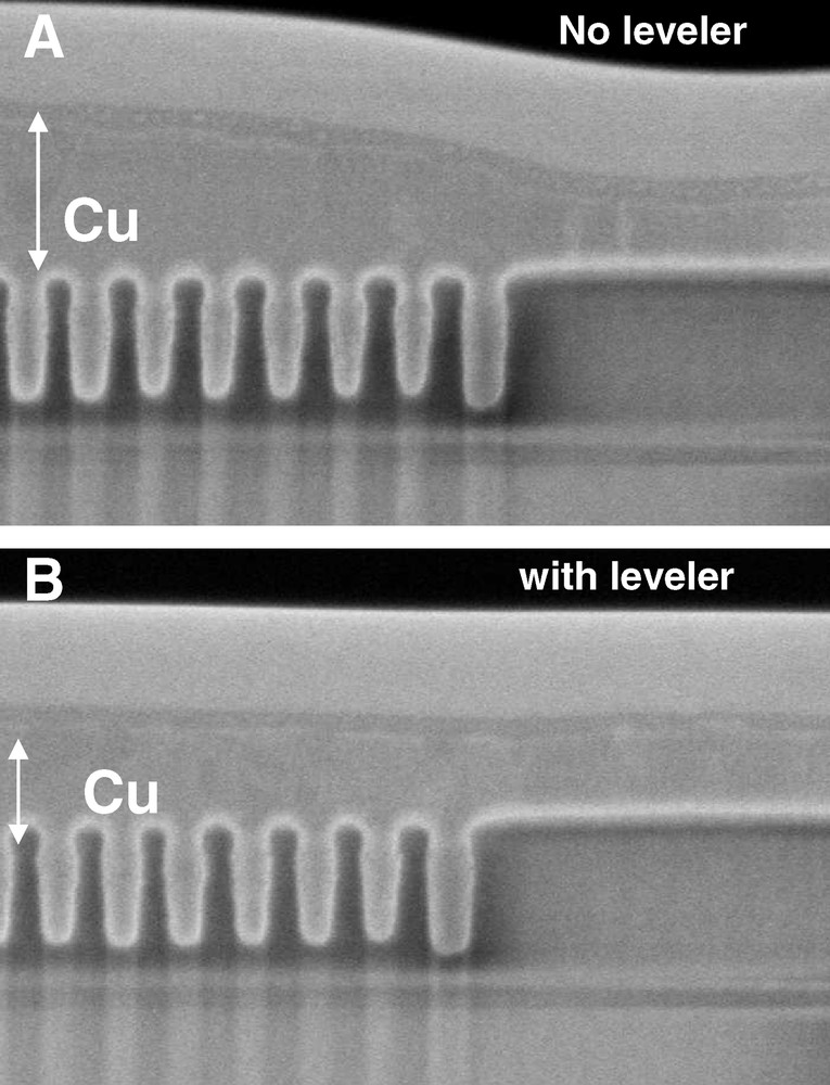
Scanning electron microscope (SEM) cross section of a dense array of Cu 50 nm lines spaced 50 nm apart (A) no leveling agent (B) with 1x leveling agent. The nominal electrodeposited Cu thickness is 150 nm. The effect of the leveling agent on the mounding is evident.
The buildup of a locally high deposited Cu thickness for densely patterned areas can have consequences in the electrical performance of such structures. In some instances, a degradation in leakage performance can be observed, as shown in Fig. 3. Leakage is an important performance characteristic that describes the flow of current between metal lines that should be separated by dielectric material. Ideally, leakage current should be very low, and is typically most difficult to control for lines that are closely spaced. Fig. 1 shows that for narrow lines that are closely spaced, a high degree of mounding can be expected. Closely spaced narrow lines thus pose not only a leakage current challenge, but a planarization one as well due to the locally high Cu thickness. Fig. 3 shows the impact of the leveler molecule concentration on the leakage current for a comb-serpentine single level structure using various leveler concentrations. Only the wafers processed in the chemistry with the nominal leveler concentration show low and tightly distributed leakage currents. The behaviour in Fig. 3 can be understood as a higher as-deposited Cu topography for the leveler-free chemistry leading to insufficient Cu planarization, resulting in a higher tendency for post-CMP Cu residuals and higher leakage currents.
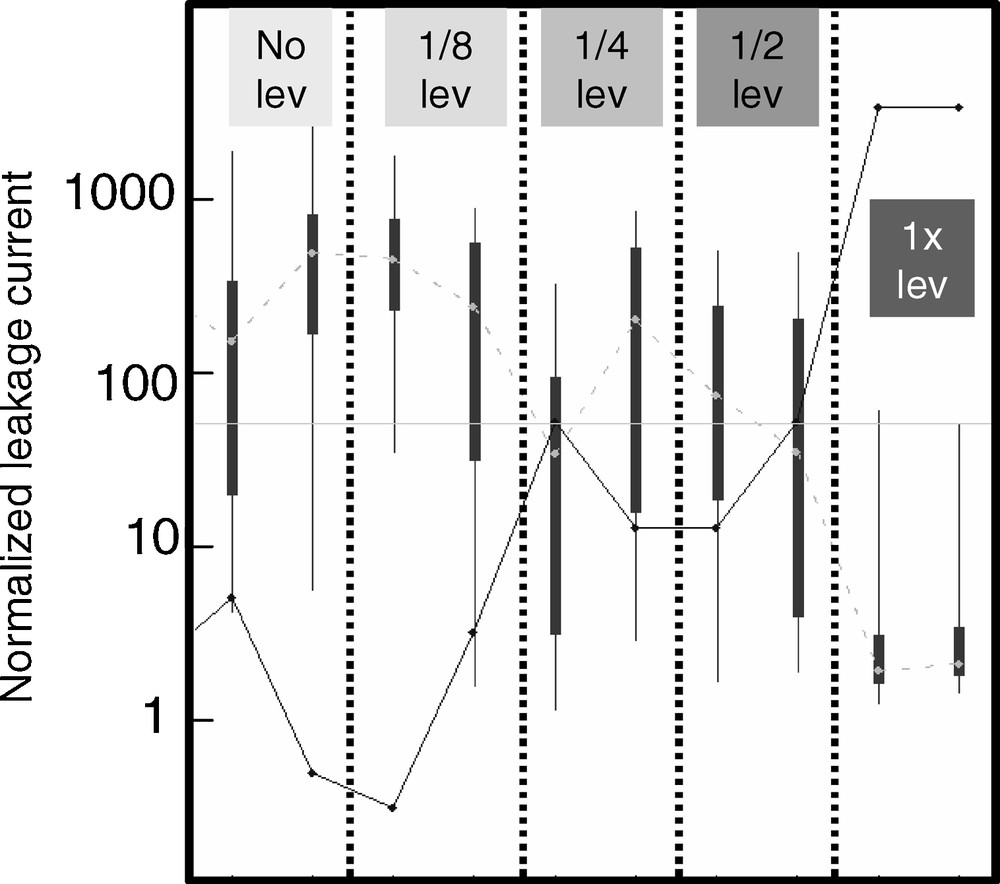
In-plane leakage current between 50 nm Cu lines spaced 50 nm apart (arbitrary units of current). Note log scale. The top and bottom of the whiskers in the plot represent 5 and 95% of the data population, respectively, while the top and bottom of the box represent 25 and 75% of the data population, respectively. The point in the middle of the box is the median value. Each set of data values is taken from a number of chips on a single 300 mm wafer. Leveler concentrations are as indicated.
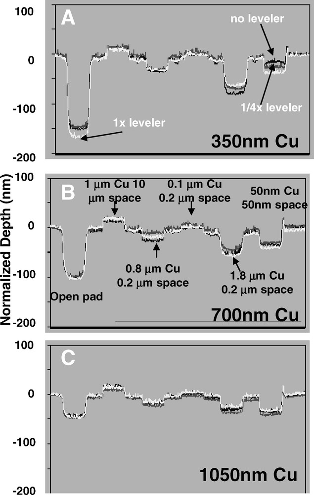
Fig. 4 shows mounding and underfill as a function of total nominal electrodeposited Cu thickness (sometimes referred to as “overburden”) for 50–50 nm line-space and 200 μm open pad structures, respectively, and different leveler concentrations. For a leveler-free electrolyte, mounding increases with Cu overburden until a thickness of about 400 nm, after which it increases less rapidly. Electrolytes having the leveler molecule exhibit in general a decreasing degree of mounding with Cu overburden thickness, with the nominal leveler concentration actually resulting in a lower local Cu thickness on the dense pattern for thicker Cu overburdens. As mentioned above, a reduction in Cu mounding can be expected to help lower the probability of within-level leakage issues.
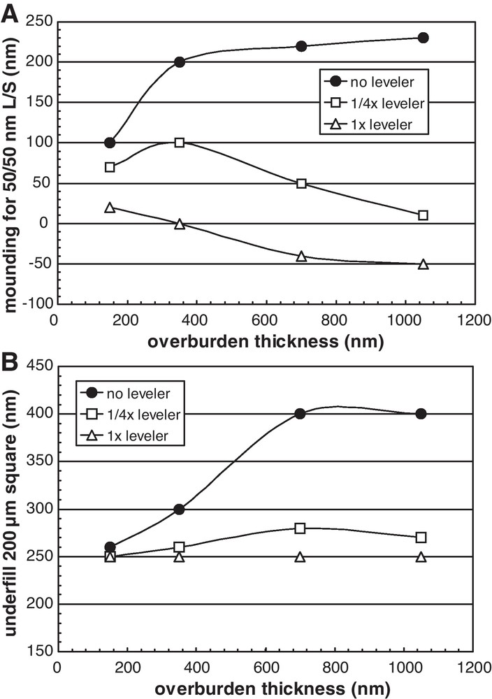
(A) Mounding of electrodeposited Cu over 50/50 nm line-space array as a function of Cu overburden for various leveler concentrations. Leveler-free electrolytes show high mounding. (B) Underfill of open 200 μm square pad as a function of Cu overburden thickness for different concentrations of leveler additive.
Although not evident in Figs. 1 and 2 where the overburden was low, Fig. 4 shows that underfill also can be mitigated by the leveler molecule, especially at higher overburden thicknesses. This is important, since depending on pattern layout and feature widths, there is a minimum Cu overburden thickness necessary to ensure that all features are fully filled with electrodeposited Cu; for Cu overburdens that are lower than this minimum value, wide features will exhibit a recess that will compromise the wafer surface planarity at that level and subsequent ones. If the relative degree of underfill can be limited by use of a leveling molecule, the minimum Cu overburden required to ensure all features are fully filled will be lower, resulting in shorter process times and lower consumable consumption for both the Cu plating and CMP processes.
Fig. 5 shows the evolution in profile during CMP for Cu electrodeposited for different leveler concentrations and various line-space combinations. The nominal Cu overburden before polish in this figure is 700 nm. Traces showing the most topography represent the beginning stages of the CMP process, and as planarization proceeds the topography evens out. The details of the curves are given in the caption for Fig. 5. What is important to note is that for the leveler-free Cu wafer, significant topography persists very nearly to the end of the CMP process. The topography appears to be removed completely just after the final Cu polish endpoint (f) step, with little further change in profile. For the cases where leveler is used, only the open pad shows significant evolution throughout the CMP process; the other line-space combinations show little change during polish, especially for the 1x leveler concentration, consistent with the idea that the as-deposited surface is already fairly planar.

Topography evolution during Chemical mechanical polishing (CMP). Traces represent (a) as-deposited, (b) 15 sec, (c) 30 sec, (d) 50 sec high downforce polish, (e) 50 sec high downforce and 50 sec low downforce, (f) Cu polish endpoint, (g) Cu overpolish, and (h) barrier polish. Nominal electrodeposited Cu thickness 700 nm, with leveler additive concentration as indicated (A) no-leveler, (B) ¼x leveler, and (C) 1x leveler. Only the Cu deposited with no leveling additive shows topography persisting throughout most of the planarization process.
This variation in topography evolution during CMP is also optically evident as illustrated in Fig. 6, where the macro scanned in Figs. 1 and 5 is shown (please note that the intent of this figure is to show how the macro-scale Cu topography evolves on these patterned areas during the Cu polish; obviously at such a low magnification, only the 200 micron wide boxes containing the various line spacing combinations are visible). The three-leveler concentrations considered in Fig. 5 are shown for the as-deposited surface, and post- 30, 50, and 100 second polish times. For the no-leveler wafer, the pattern is clearly visible throughout the CMP process, except for the post- 100 sec image (though some contrast is still visible in this image, suggesting the surface has not been completely planarized). For the 1/4x leveler case, the pattern becomes invisible after 50 sec of polish; after 100 sec, the pattern appears to start to become visible again, presumably since Cu at this point is nearly completely removed, revealing the liner beneath the Cu in some places. The case of the nominal leveler concentration is similar to the 1/4x case, except that the as-deposited surface shows less contrast, as expected for a smoother surface. At 100 seconds of polish time, the Cu is now clearly almost entirely removed, with the pattern again becoming visible.
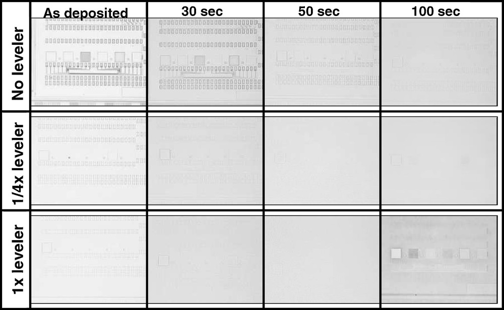
Optical micrographs of profiled area during selected points during the Cu polish process with leveler concentration as indicated (at this magnification only the boxes containing the areas having various line and spacing are visible, not the individual lines themselves). Nominal electrodeposited Cu thickness for images shown is 700 nm. Field of view in each image is approximately 2 mm.
Fig. 7 shows the final post-CMP topographies for different leveler concentrations and overburden thicknesses. Some variation in topography with leveler concentration on the dense patterns and open pad is evident for the 350 nm Cu overburden. For the thicker overburdens, the leveler concentration doesn’t appear to strongly influence the final post-CMP topography. This is interesting, since the results in Fig. 3 show that although the final post-CMP topography may be similar for different leveler concentrations (Fig. 7), the resulting leakage performance may be strongly influenced by the presence of the leveler molecule. This suggests that leakage could be caused by highly localized defects such as small particles or locally inadequate planarization of the Cu, resulting in Cu residues that may be missed in a profilometry scan. Another aspect to note in Fig. 7 is that the final post-CMP recess in the open pad appears to be mainly related to the Cu overburden thickness. This suggests that although the leveler may help mitigate as-deposited underfill, the final amount of post-CMP recess (or “dishing”) in wide features is strongly influenced by the Cu overburden thickness.
Final post-chemical mechanical polishing (CMP) topography for different leveler concentrations and overburden thicknesses, with line spacing as indicated. Some differences in post-CMP topography with leveler concentration are apparent for the thinnest Cu overburden.
Fig. 8 shows the wafer scale thickness evolution for different leveler and Cu overburden thicknesses. The average Cu thickness was determined by sheet resistance measurements across the wafers at various points in the CMP process. A “bulk copper removal”, or high-down force (HDF) initial polish step having a fast Cu removal rate is typically used to first rapidly thin the Cu down to a low thickness. The HDF time for the Cu planarization process was adjusted to account for the different Cu overburden thicknesses, with longer HDF times used for the thicker overburdens. A “copper clearing”, or low-down force (LDF) step with a slower Cu removal rate followed the HDF one to clear the last remaining layer of Cu in a controllable fashion. This approach of a HDF step followed by a LDF one is typical for a Cu CMP process. Note for the 350 nm overburden the time scale is compressed, reflecting the shorter CMP times associated with thinner overburdens. The dispersion in the thickness vs. time curves for the different leveler concentrations is evident, with the wafers from the no-leveler chemistry taking longer to planarize. The difference between wafers from the ¼x and 1x leveler chemistries is less obvious, especially for the thicker overburdens, but a consistent trend of the 1x leveler polishing the most rapidly is visible.
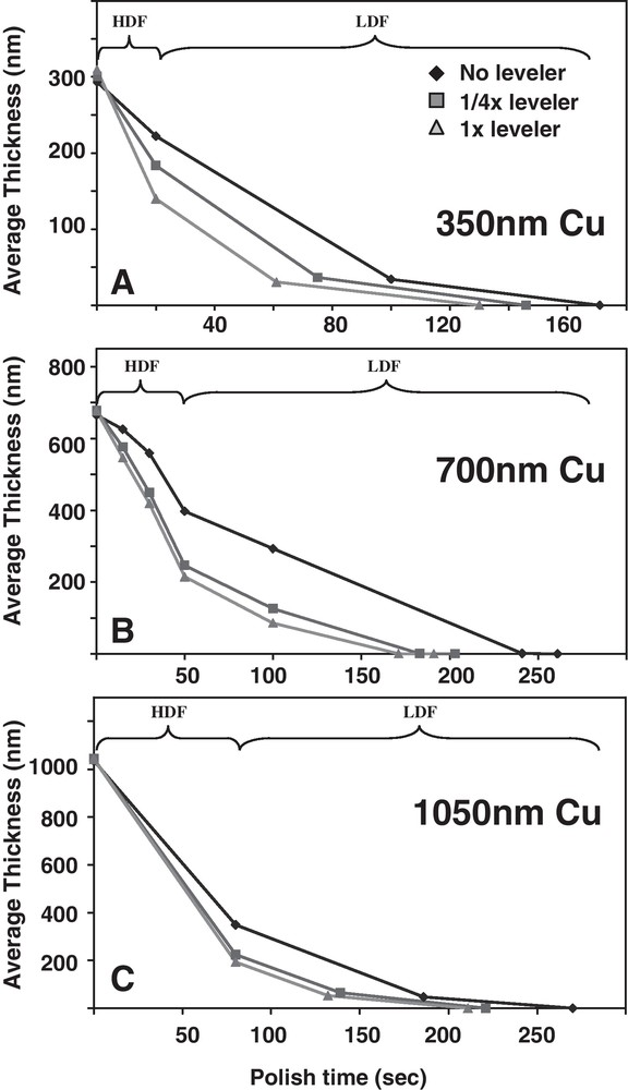
Average wafer scale Cu thickness as a function of polish time for leveler and Cu overburden as indicated (A) 350 nm Cu overburden, (B) 700 nm Cu overburden, and (C) 1050 nm Cu overburden. The high-down force (HDF) time was adjusted to account for the total Cu overburden thickness. “LDF” indicates low down force Cu polish step. For lower overburdens, the difference in Cu thickness evolution is more obvious.
The average Cu removal rates for both the HDF and LDF polish steps are shown in Fig. 9 for the corresponding leveler concentrations and Cu overburdens in Fig. 8. It is evident that the LDF steps all seem to be independent of leveler concentration, consistent with the idea that most of the topography is eliminated in the HDF step. As expected based on the curves in Fig. 8, the average HDF removal rate is lower for wafers processed with the leveler-free chemistry; the differences in HDF removal rate with leveler concentration become more significant for the lower Cu overburdens, consistent with the idea that for the shorter HDF times, a larger fraction of the time will be spent removing topography compared to the longer HDF times used for thicker overburdens (another aspect consistent with this observation is that in Fig. 4, it was shown that mounding for the leveler-free chemistry plateaus after 400 nm Cu overburden, meaning the degree of excess Cu topography relative to the overburden thickness is most extreme at low overburdens when no-leveler is used). These data show that the average Cu polish rate is dependent on the incoming electrodeposited Cu topography, especially for thinner Cu overburdens.
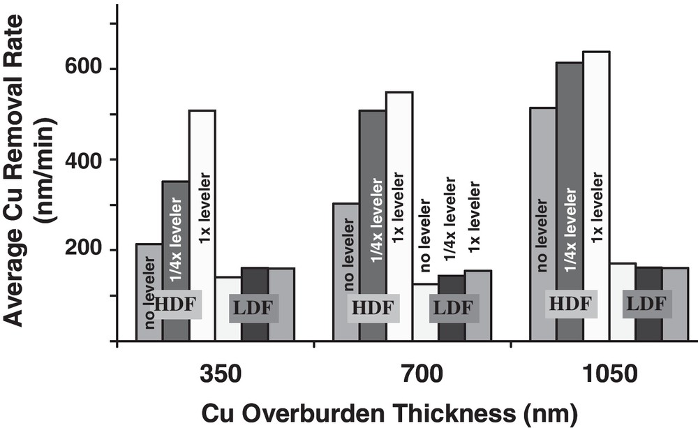
Effective high and low down force (HDF and LDF, respectively) Cu polish rate for different leveler and Cu overburden thicknesses (for LDF, only the 700 nm overburden thickness leveler concentrations are indicated for readability; the other overburdens are plotted in the same order). The differences in HDF Cu removal rate in the step with leveler concentration are more evident for the thinner overburdens.
In this study, the effect of a typical leveling agent on electrodeposited Cu topography and its impact on the subsequent CMP process was considered. Although not considered here, it is evident that this leveling additive should not interfere with the function of the other additives present in Cu damascene chemistries, the suppressor and accelerator molecules that provide proper bottom-up filling [8–21]. Such interactions could be interesting topics for further study.
4 Conclusions
The impact of Cu leveling additives on electrodeposited Cu topography and subsequent planarization behaviour was studied on both the pattern and wafer scales. The presence of a leveling agent significantly reduces mounding and to a lesser degree underfill. This results in a higher effective Cu removal rate during subsequent CMP processing, both at the pattern and wafer scales. On the wafer scale, this effect is more evident for lower overburdens as a larger fraction of the total polish time is spent removing the excess topography. On the pattern scale, significant topography persists throughout almost the entire CMP process when a leveling additive is not used, while only very wide features (∼ > 100 μm) show appreciable topography evolution for Cu deposited with a leveling agent. Excess electrodeposited Cu topography can lead to insufficient Cu planarization, resulting in in-plane leakage between Cu damascene features.
Acknowledgements
This work was performed by the Research Alliance Teams at various IBM Research and Development Facilities.