1 Introduction to plasmas, cold plasmas and plasma–surface interactions
Plasmas, which are also called the fourth state of matter, are defined as a partially ionised gaseous medium. Physicists usually classify plasmas according to the characteristics of the charged particles, their number density and their average kinetic energy, the latter being frequently expressed as an average temperature (Fig. 1).

Plasma temperature versus number density diagram. Man-made cold plasma region is indicated by the yellow box. Adapted from Ref. [1]. Copyright 2010, Contemporary Physics Education Project.
Man-made cold plasmas, which are used for material processing, have the specificity to be out of thermodynamic equilibrium: average energy of the electrons (Te) typically ranges from 0.1 to 10 eV (∼103–105 K), whereas the neutral and ionised species are at “room” temperature (300–600 K, i.e., 0.025–0.050 eV) or close to it. Typical density (i.e., electron density, Ne) is in the range of 1014–1018 m−3. Depending on the mode of plasma generation and the application, the operating pressure is usually between 0.1 mTorr and 1 atm (∼10−1–105 Pa).
In plasma processing, the plasma is used as a chemical reactor providing the desirable species and some others. The energy fed to the electrical discharge is gained by the electrons, which allows them to initiate dissociation, ionisation or attachment reactions with the molecules, radicals or atoms for the sake that their energy is above the corresponding cross-section threshold. As an example, Fig. 2 presents cross-sections for various electron-induced processes on CF4 [2]. Typical reactions are as follows:
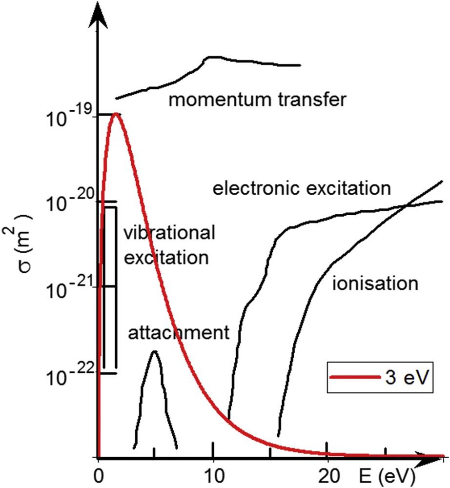
Electron-induced cross-sections for CF4. Also shown is an energy distribution for Te = 3 eV electrons. Adapted from Winters et al. [2]. Copyright 1982, APS Publishing.
A plasma created from polyatomic molecules is thus composed of the mother molecule, atoms, radicals, electrons, positive ions, and eventually negative ions. Generally, the produced species are not in their fundamental states, so the system glows in the UV–visible–IR range due to the photons emitted by radiative de-excitation of the excited species. In the volume of the plasma, the overall system is electrically neutral as the number of positive ions equals to the number of negatively charged species (electrons + negative ions). Comparing the electronic excitation and ionisation cross-sections to a typical electron energy distribution (Te = 3 eV) allows one to specify an important feature: plasma chemistry is induced by the few electrons of the high energy tail of the distribution. The low energy electrons control the collective behaviour of the plasma and the equilibrium with the surfaces. Information on the plasma composition and electrical characteristics can be obtained by means of mass spectrometry [3–7], optical spectroscopy (emission [4–6] or absorption [8]) and electrostatic probes [6,7,9].
The way the plasma species interact with the sample material defines the dominating operating process. For example using a CF4 plasma, fluorocarbon radicals (CFx) can generate a fluorocarbon layer; alternatively fluorine atoms will etch silicon via the formation of volatile SiF4. Another important element is the (positive) ion bombardment at the surfaces. Due to the difference in the mobility between electrons and positive ions, the collective behaviour of the plasma leads to a positive potential of the plasma volume with respect to all surfaces. A space charge sheath is thus formed between the plasma and the surface, in which the average electrical field accelerates the positive ions towards the surface and repels the electrons. Biasing the sample holder using an rf bias at a frequency (usually 13.56 MHz) higher than the ion plasma frequency allows us to control the average voltage drop (denoted as self-bias) between the plasma and the material, and thus the average energy of the bombarding ions. The result of the interaction between the plasma and the material to be treated will thus depend on the following main features [10]:
- • the nature of the species produced by the electron-induced processes through the choice of the feed gas;
- • the flux of these chemical active species onto the sample via the pressure and power fed to the discharge;
- • the flux of positive ions via the power fed to the discharge and the operating pressure;
- • the energy of the bombarding ions via the bias power applied to the sample and the operating pressure.
Potential applications range from thin film deposition, etching features using a mask to protect part of the surface that should not be etched and surface treatment. The latter domain is very broad as it includes engineering of surface morphology (roughening, smoothing, nanostructuring, etc.), engineering of surface chemistry (cleaning, grafting, etc.) or in-depth chemistry (ion implantation) and biomedical applications (sterilisation of surgical tools, tissue and wound healing, etc.). Characterisation of the plasma process makes use of numerous techniques. Imaging techniques such as secondary electron microscopy (SEM), transmission electron microscopy (TEM) and atomic force microscopy are commonly used to gain information about the surface and pattern morphology and topography. Surface analyses such as X-ray photoelectron spectroscopy (XPS) [11–15], Auger electron spectroscopy [16,17] and energy dispersive spectroscopy coupled with TEM bring information on the surface chemistry. Secondary ion mass spectrometry, Fourier transform infrared spectroscopy [18], Raman spectrometry and ellipsometry [19] provide information on thin film composition and structure, and in-depth modification of the material.
2 Fluorine plasmas for etching—principles of plasma etching and pattern transfer
2.1 Basic principles of plasma etching
Plasma species will etch a material whenever their interaction condition with the surface leads to the formation of a stable volatile compound [20] and in fine matter removal. A first-order guide to determine what kind of a material could be etched in fluorine-based plasmas as compared to other halogen-based chemistries is to consider the boiling point of the stable products. As seen from Table 1, fluorine plasmas will etch easily elements in column 14 (C, Si, Ge, etc.) as well as tungsten and can also be used for titanium or tantalum. On the contrary, III–V semiconductors, aluminium and hafnium will require chlorine or bromine. Titanium should etch easier using chlorine than fluorine; alternatively, chlorine and bromine chemistries can also be used to etch silicon and germanium.
Boiling points (BPs) for some stable halogenide compounds of elements present in the most common materials used in microelectronics, optoelectronics and photonics [21].
| Element | Fluoride | BP (°C) | Chloride | BP (°C) | Bromide | BP (°C) |
| B | BF3 | −100 | BCl3 | 12 | BBr3 | 3 |
| Al | AlF3 | 1297 (sub) | AlCl3 | 178 (sub) | AlBr3 | 263 |
| Ga | GaF3 | 1000 | GaCl3 | 201 | GaBr3 | 279 |
| In | InF3 | >1200 | InCl3 | 300 (sub) | ||
| P | PF3 | −101 | PCl3 | 75 | PBr3 | 173 |
| PF5 | −75 | PCl5 | 162 (sub) | PBr5 | 106 | |
| As | AsF3 | −63 | AsCl3 | 130 | AsBr3 | 221 |
| AsF5 | −53 | |||||
| Sb | SbF3 | 376 | SbCl3 | 220 | SbBr3 | 288 |
| SbF5 | 141 | |||||
| Si | SiF4 | −86 | SiCl4 | 58 | SiBr4 | 154 |
| Ge | GeF4 | −37 (sub) | GeCl4 | 84 | GeBr4 | 187 |
| Ti | TiF4 | 184 (sub) | TiCl4 | 136 | TiBr4 | 230 |
| Ta | TaF5 | 230 | TaCl5 | 242 | TaBr5 | 349 |
| W | WF6 | 17 | WCl6 | 347 | WOBr4 | 327 |
| WOF4 | 188 | WOCl4 | 228 | |||
| Hf | HfF4 | 970 | HfCl4 | 317 | HfBr4 | 323 |
| Cd | CdF2 | 1750 | CdCl2 | 960 | CdBr2 | 863 |
| Se | SeF6 | −47 | ||||
| SeF4 | 102 | SeCl4 | 191 (sub) | |||
| Te | TeCl2 | 328 | TeBr2 | 339 | ||
| TeF4 | 195 | TeCl4 | 387 | TeBr4 | 420 | |
| TeF6 | −39 |
Thus, the typical materials concerned by fluorine plasma etching and sorted according to their application are as follows: transistor gate (poly-Si); interlevel dielectrics (SiO2 and organosilicon low-k); spacers (SiO2 and Si3N4); hard masks (SiO2 and organosilicon polymers); microelectromechanical system (MEMS), microopticoelectromechanical system (MOEMS) (Si, SiO2, Si-based oxide glasses, organosilicon polymers); IR photonic devices (SiO2, chalcogenide glasses); phase change random access memory (RAM) (chalcogenide compounds) and surface functionalisation (polymers).
The most common gases used as a source of fluorine are presented in Table 2. The most widely used, SF6, CHF3, CF4 and C4F8, are nontoxic, in case of a leak their only risk of use in a closed space is thus asphyxia by substitution to air because of their higher density. Their main care of use concerns their high global warming potential and long atmospheric lifetime. These gases should not be rejected in the atmosphere.
Some characteristics of the main feed gases used in fluorine plasma processing.
| Gas | ANSI/ASHRAE Nomenclature | Density (g/L @ 25 °C) | Toxicity (ppm) | Flame | GWP (100 y) | Lifetime (y) |
| SF6 | 6.17 | Nontoxic | Nonflammable | 23,900 | 3200 | |
| CF4 | R-14 | 3.72 (15 °C) | Nontoxic | Nonflammable | 6500 | 50,000 |
| CHF3 | R-23 | 2.95 (15 °C) | Nontoxic | Nonflammable | 11,700 | 270 |
| CH3F | R-41 | 1.44 | Narcotic | F+ | 150 | 4 |
| C2F6 | R-116 | 5.73 | Nontoxic | Nonflammable | 9200 | 10,000 |
| C4F8 | C-318 | 8.82 (15 °C) | Nontoxic | Nonflammable | 8700 | 3200 |
| NF3 | 3.00 (15 °C) | 10 | Nonflammable | 17,200 | 740 |
Due to the presence of CFx radicals that tend to produce fluorocarbon films, fluorocarbon-based plasmas behave very differently from SF6, for instance, when interacting with silicon and SiO2 materials. For example, Fig. 3 reports a typical evolution of the etch rate (ER) of Si and SiO2 in CHF3 high-density plasma and that of SiO2 in Ar high-density plasma, when varying the average bias voltage (given here in absolute value) applied to the sample holder. Other examples can be found in Refs. [6,22,23]. The first important feature is that the ER of SiO2 in CHF3 plasma is typically one order of magnitude greater than in Ar, although the ion flux is typically one order of magnitude lower. This illustrates the importance of chemical reactions in reactive plasma etching processes. The second important feature is that both Si and SiO2 etching in CHF3 require applying a sufficient bias (typically above 100 V) to be effective. Indeed, below 50 V the ion bombardment is not sufficiently energetic to inhibit the formation of a fluorocarbon film at the sample surface and the dominant process is fluorocarbon deposition. The third feature is the significantly larger ER of SiO2 as compared to Si because of the difference in material composition: in the case of Si, XPS and Auger electron spectroscopy analyses show that the etching proceeds through a thin (few nanometres) fluorocarbon layer [17,24] that takes part in the etching mechanism [25]. ER varies typically as the inverse of the layer thickness [13,26]. In the case of SiO2, the oxygen atoms freed by the energetic ion bombardment react with the incoming CFx radicals, producing stable CO, CO2, COF2 species as volatile etch products and prevent the development of such a layer. This situation allows us to achieve selective etching of SiO2 with respect to Si [5,23,27]; the process can be tuned by the operator by changing the gas mixture: adding O2 will counterbalance the tendency to fluorocarbon deposition [28], whereas addition of H2 will scavenge fluorine and promote the formation of fluorocarbon deposition [29].

ER of Si and SiO2 in CHF3, and SiO2 in Ar plasma versus the applied bias to the sample holder. Other conditions: 800 W plasma power, 10 mTorr pressure and 40 sccm total gas flow.
In SF6 plasmas, SFx radicals do not lead to film deposition. Therefore, pure chemical etching, i.e., without bias becomes possible. Fig. 4 shows that a very efficient etching is obtained for Si because of the high concentration of fluorine atoms produced in SF6 plasma as compared to fluorocarbon gases. On the contrary, nearly no etching is observed for SiO2. The reason is that energetic ions are necessary to break the strong SiO bonds and allow chemisorption of fluorine atoms on silicon sites. The advantage of this situation is the possibility to etch selectively Si with respect to SiO2.

ER of Si and SiO2 in CHF3 and SF6 plasma versus plasma excitation power. Bias conditions are −200 V for CHF3 and no bias for SF6. Other conditions: 10 mTorr pressure and 40 sccm total gas flow.
In summary, SiO2 etching needs ion assistance and it can be considered as the “text book case” for ion-assisted chemical etching, whereas Si presents a typical purely chemical etching behaviour with fluorine atoms, although its etching will benefit from ion assistance if it is added. Ion-assisted chemical etching can be modelled considering Langmuir adsorption kinetics [30]. Assuming a stationary situation, the time variation of the surface coverage in fluorine (θ) is expressed as
| (1) |
Besides, the ER (in atoms s−1 or molecules s−1) is expressed as:
| (2) |
Neglecting purely physical etching (see Fig. 3) and purely chemical etching (see Fig. 4) and extracting θ from Eq. (1), the ER simplifies to
| (3) |
Considering the etch yield (EY) per electronvolt (number of atoms etched per incident ion per electronvolt)
| (4) |
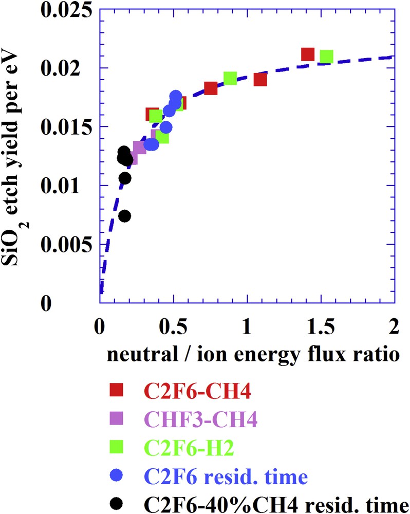
SiO2 EY per electronvolt versus the active neutral species to ion energy flux ratio when varying the gas mixture in C2F6CH4, CHF3CH4, C2F6H2 or varying the total gas flow rate (residence time) in C2F6 and C2F640%CH4. Ion energy is 170 eV when varying the residence time and 220 eV when varying the gas mixture.
Yet, one can consider an alternative model in which the ions not only induce sputtering processes but are also responsible for chemical reactions [34]. In such case of direct reactive ion etching one expects a dependency of the etching yield on the chemical composition of the ions. If one takes into consideration the composition of the CFx+ ions when varying plasma conditions as in Fig. 5, a dependency is indeed also observed in relation to the F/C ratio (Fig. 6) [35].
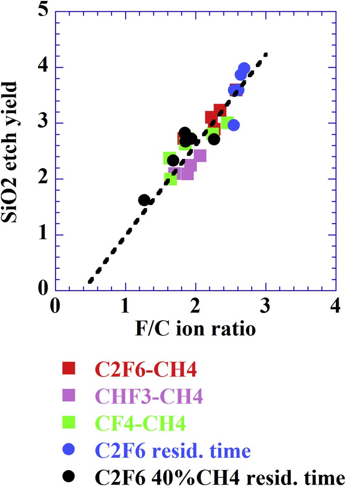
SiO2 EY versus the F/C ratio determined from the ion composition when varying the gas mixture, pressure (5 and 10 mTorr) and residence time (75–750 ms). Ion energy is 170 eV when varying the residence time and 220 eV when varying the gas mixture.
In conclusion, separating the contribution of neutral species from that of ionized species in reactive plasmas is all but trivial.
2.2 Principles of pattern transfer
In the perspective of pattern etching, the directional ion bombardment perpendicular to the surface is essential as it brings a physical contribution and enhances etching in this direction with respect to lateral etching that will be purely chemical. Etching anisotropy (A) is defined as the ratio between the perpendicular (ion-assisted) and lateral (purely chemical) ERs through the following relation: . Accuracy of the pattern transfer with respect to the mask design, slope of the sidewall, etch selectivity with respect to the mask and to the underlayer, damage to the pattern bottom, and surface chemistry at the sidewall and pattern bottom will therefore depend on plasma parameters such as the ion flux and energy, the nature of the neutral species and their respective flux, as well as the flux ratio between neutral and ionic species. Other key points are the mask resistance to the plasma, the need for ion assistance and its efficiency, and the possible competition between etching and deposition processes.
In parallel, lateral etching is kept low by two concurrent mechanisms. First, the ion assistance is low because of the low ion flux at the sidewall. Second, whenever the plasma produces species that tend to form deposits, as in the case of fluorocarbon plasmas with CFx species, or species that can react at the sidewall to form a resistant layer, these species contribute to the protection of the pattern sidewall by forming a passivation surface layer.
2.3 Recent developments in plasma etching processes
Control of pattern dimension and damage to the materials being more and more stringent with the evolution of technology, new plasma processes need to be invented permanently for a better control of the ion flux and ion energy. This has led to pulsed plasma processes, in which the duty cycle (dc) offers an efficient knob to tune the plasma dissociation and the ion flux and energy to the substrate [36]. It has led also to pulsed bias processes in which the ion energy to the substrate is tuned, whereas the ionic and neutral species fluxes remain constant [37]. Finally, it has led also to alternated or pulsed gas processes, with efficient progresses in deep etching [38,39] and atomic layer etching [40,41].
In parallel, tremendous work has been done throughout the years on the modelling of plasma chemistry [42], plasma–surface interaction and etching mechanisms [30,43], as well as pattern transfer [44].
The examples given hereafter do not pretend providing a complete review of the intense research that has been carried out since the origin of plasma processing of materials, nor presenting an exhaustive panel of materials, processes and application. Objective is to give the reader an idea of the variability of the application of fluorine plasmas and to bring further explanations about etching mechanisms and also illustrate some recent advances in plasma processing.
3 Examples in microelectronics
3.1 Gate technology
3.1.1 Gate etching—evolution through the history of microelectronics
In the early days of Si-complementary metal oxide semiconductor (CMOS) technology (1975–1990), the main materials to be etched were Si for the transistor gate and SiO2 for the interlevel dielectric. Processing reactors were capacitively coupled diode systems in which the sample is placed onto the rf-powered electrode. In such systems the feed power acts on both the plasma density and the electrode bias with respect to the plasma. Therefore, ion flux and energy are not independent parameters. Moreover, the operating pressure is relatively high (typically above 50 mTorr), so the ions encounter several collision processes during their transport through the sample sheath, which reduces their effective energy, degrades their energy distribution towards low energies and increases their angular distribution.
Such systems operate efficiently in fluorocarbon gases; self-bias up to 250 V can be obtained in a pressure range of 50–200 mTorr. They were used to achieve selective etching of SiO2 with respect to Si [45] and anisotropic etching of SiO2 interlevel layers. Si etching was also attempted in CF4O2, for instance, to avoid the formation of a fluorocarbon-blocking layer, yet patterns presented a severe lack of anisotropy [46]. In SF6, only low self-bias values are obtained (∼20 V) because of the high affinity of SFx radicals for electron attachment and the subsequent low electron density and high proportion of negative ions. Therefore, selective etching of the poly-Si gate with respect to the gate oxide was possible, but in the absence of passivating species to protect the sidewall and of ion assistance to increase perpendicular etching with respect to lateral etching, patterns were essentially isotropic.
With the increasing demand of higher integration and the need for smaller pattern dimensions, greater dimension control and high selectivity with respect to the gate oxide, fluorine-based plasmas were abandoned for poly-Si gate etching to the profit of chlorine- or bromine-based chemistries. Cl2 and HBr plasmas allow selective etching of Si over SiO2 [47] and the much slower chemical etching of silicon with Cl and Br as compared to F favours pattern anisotropy. Difference in the chemical etching of Si with F and Cl atoms, as well as the absence of chemical etching with Br atoms can be explained by steric effects [48]. Assuming a Langmuir–Hinshelwood surface reaction model, chemical etching and formation of a SiX4 (X = F, Cl, and Br) product require a surface coverage in X atoms larger than 3/4 [16,49]. Considering a 〈100〉 crystalline silicon surface as a model means that X should be able to occupy simultaneously the two dangling bonds of two adjacent Si surface atoms. Taking into account the lattice parameter a = 5.43 Å, this will be only possible if the X atom covalent radius (RCX) is smaller than (or just above at the cost of a slight twist of the bond orientation) [50]. As shown in Fig. 7, this is encountered only for F (RCF = 0.64 Å) and Cl (RCCl = 0.99 Å), but not for Br (RCBr = 1.14 Å) and a fortiori I (RCI = 1.33 Å). In addition, chemical etching is far more effective if the X species can diffuse inside the lattice, leading to multilayer adsorption [51] (in such case the reaction model is closer to an Eley–Rideal model). For a 〈100〉 Si surface this is only possible if the X− ionic radius (RX−) is smaller than , with RTC the tetrahedral covalent radius for Si [52]. Only F meets this requirement (RF− = 1.33 Å) and thus presents an intrinsic isotropic etching of Si (Fig. 7a).
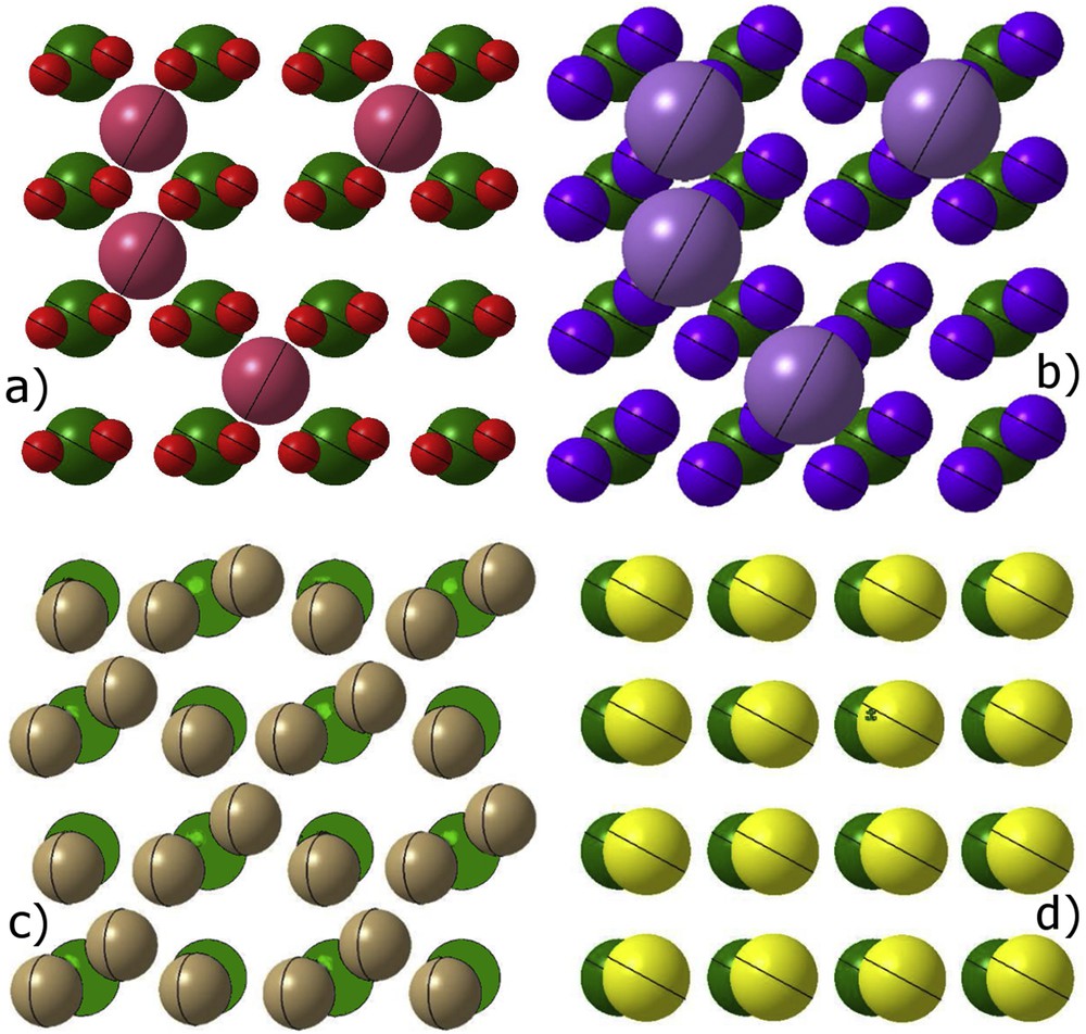
Si 〈100〉 (top view) saturated with (a) fluorine, (b) chlorine, (c) bromine and (d) iodine atoms. Si atoms are in green, F atoms in red, Cl atoms in blue, Br atoms in beige and I atoms in yellow. According to the model chemical etching is only possible with F and Cl, etching with Br requires ion assistance (no chemical etching), I etching is not possible. F atoms occupying a tetrahedral inner site are in pink, Cl atoms attempting to occupy a tetrahedral site are in violet. Adapted with courtesy from Phan [50].
So during the years 1990s and 2000s, as the technology nodes shrunk from 0.6 μm down to 45 nm, poly-Si gate etching has been achieved using Cl2 [12,53], HCl [54], HBr [55], HBrO2 [56] or HBrCl2O2 [57] or gas mixtures. Efficient pattern transfer and control of pattern dimension were obtained due to the formation of a SiOxCly or SiOxBry passivation layer at the feature sidewall. This layer, typically 4–8 nm thick, is built on deposition and oxidation of rather weakly volatile etch products.
In parallel, during the year 1990s, new plasma systems were invented: electron cyclotron resonance microwave plasma sources and rf inductively coupled plasma sources allowed one to produce much denser plasmas (Ne ∼1010–1012 cm−3) at lower pressures (1–20 mTorr). Plasma excitation being now independent of sample bias, the ion flux could be decoupled from the ion energy. Moreover, operating at low pressure allowed us to increase the flux ratio between ionised species and neutral species, and by decreasing the collision frequency between these species during the transport through the sheath in front of the sample, it increased the ion flux directionality and narrowed its energy distribution. In principle, this should increase anisotropy; however, a much denser plasma also leads to a higher degree of dissociation. In fluorocarbon plasmas, the concentration ratio between fluorine atoms and CF2 radicals thus increased in high-density plasmas as compared to capacitively coupled plasmas. The result is an important increase in the ER of Si, but to the cost of a loss of anisotropy, and selectivity to resist masks.
Alternatively, progress was also made in capacitively coupled plasma sources with the use of bifrequency excitation on the sample electrode. For example, a power delivered at high frequency (∼40 MHz) can control the plasma density and thus the ion flux, and one delivered at a lower (usual) rf frequency (13.56 MHz) will tune the sample self-bias and the ion energy [58].
Going down to 32 and 20 nm in the mid-2010 required to reduce the thickness of the sidewall passivation. A recipe based on the deposition of weakly volatile etch products was no more compatible with further reduction in dimension. Solution was found in the return of fluorine in the etching chemistry! Processes were developed using SF6–hydrofluorocarbon–N2He mixtures [59]; the role of the hydrofluorocarbon (CHF3, CH2F2, etc.) is to produce CFx radicals allowing the formation of a passivation layer [14] and that of N2 is to limit the development of this layer [60]. Figs. 8 and 9 illustrate the evolution of the control of these passivation layers.
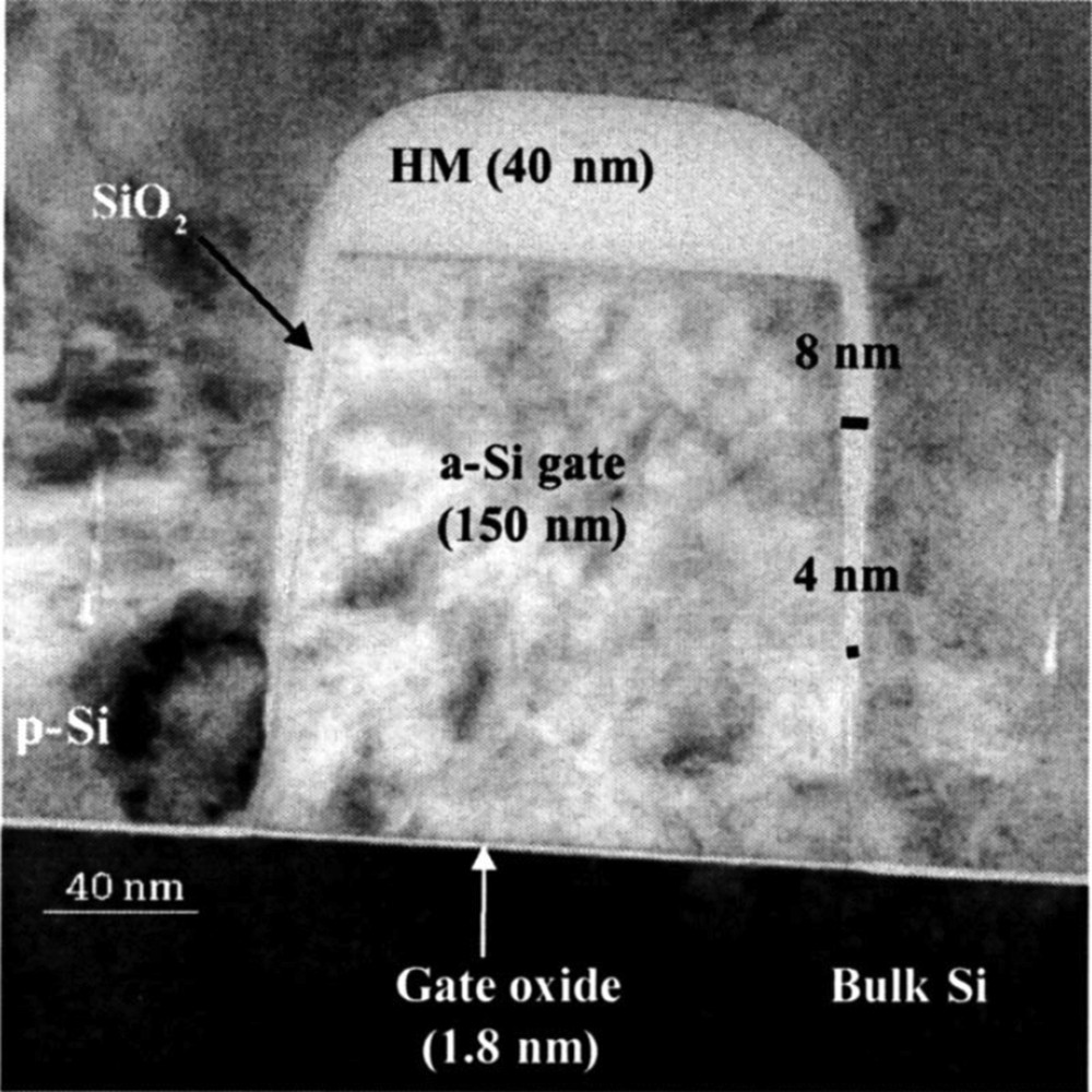
Poly-Si gates etched in HBrO2, the sidewall passivation layer (SiOxBry) varies from 4 to 8 nm. Reproduced with permission from Desvoivres et al. [61]. Copyright 2001, AVS Publishing.
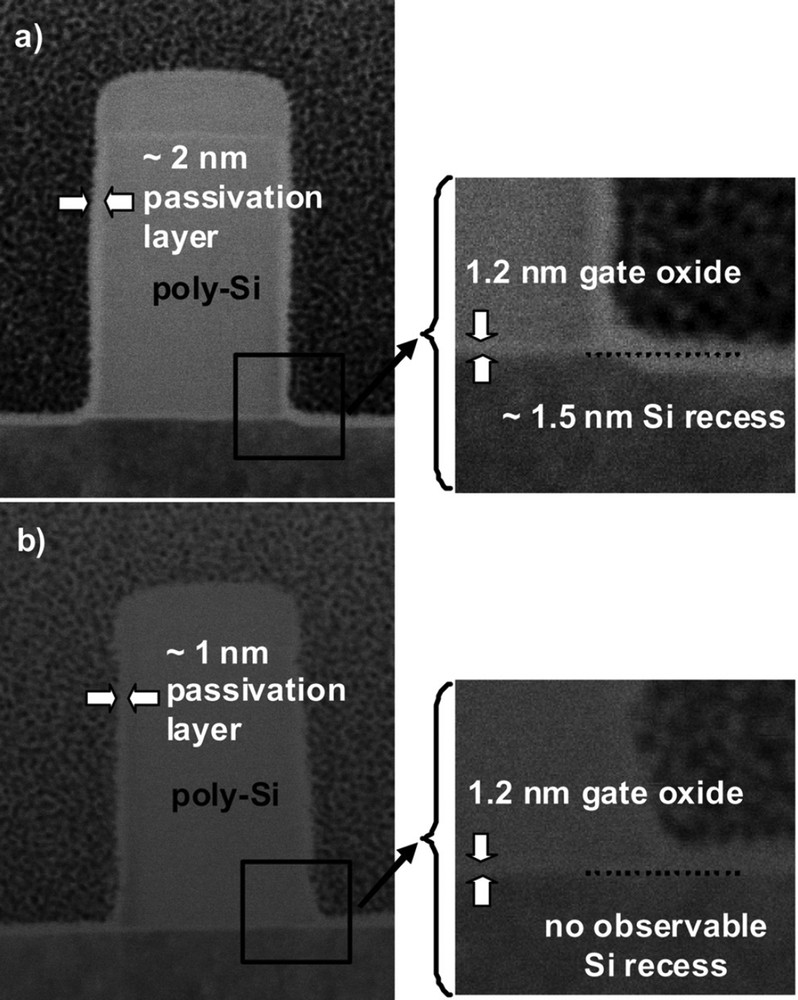
Poly-Si gates etched in SF6CHF3N2He, the sidewall passivation layer (fluorocarbon) is only 2 nm (a). Synchronous pulsing during the overetch in HBrO2 avoids damage to the Si active regions (b). Reproduced with permission from Petit-Etienne et al. [59]. Copyright 2012, AVS Publishing.
However, soft landing on the gate oxide and overetch sequences are carried out in HBrO2 and at a higher pressure to limit as possible the degradation of the oxide (1.2 nm only) and of the Si substrate underneath that will cause undesirable Si recess. Pulsing the plasma and the bias synchronously during the overetch steps brings a significant progress (Fig. 9) [59].
3.1.2 Mask technology at the nanoscale
Design of gates at the nanometre scale (typically 32 nm and less) requires the realization of the corresponding mask. Creating patterns in a photoresist at a pitch smaller than 70 nm are beyond the limits of deep UV (DUV) lithography operating at 193 nm. Complex technological processes have been invented to overcome this situation. One of them is called self-aligned double patterning (Fig. 10). After the lithography step (pitch 80 nm) and a slimming of the resist pattern (Cl2/O2 or HBr/O2 plasma) by a factor 2, the patterns are covered with a conformal SiO2 layer, called the spacer, with a thickness (20 nm) adjusted to be equal to one-quarter of the initial pitch. Then a highly anisotropic etching step is carried out (spacer etch) by means of a fluorocarbon-based plasma, this allows us to eliminate the SiO2 layer at the top and bottom of the features and keep only the layer along the resist sidewall. Second, the resist is removed: the initial resist mask at a pitch of 80 nm is replaced by a SiO2 mask at a pitch of 40 nm. This mask is further used to pattern the underlayers, Si-ARC and SOC that constitute the hard mask [62]; Si-ARC etching also involves fluorocarbon-based plasmas. Triple and quadruple patterning schemes have also been invented [63].
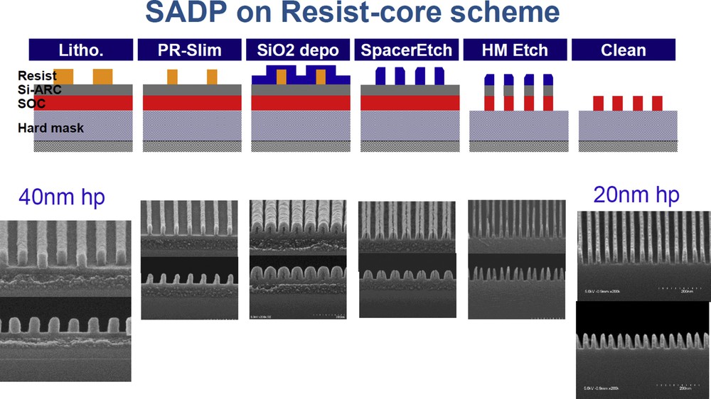
Process scheme for self-aligned double patterning (SADP). Adapted from Yaegashi [63].
3.1.3 Spacer etching
A dielectric spacer, usually made of Si3N4, is also necessary around the gate to precisely define the channel length below the gate. Processes for spacer etching “are one of the most critical steps of transistor fabrication technologies since they must be at the same time very anisotropic to generate straight spacer profiles and extremely selective to silicon in order to minimize the silicon consumption in source/drain regions. Minimizing the silicon recess and ion-induced damages to silicon surfaces are key criterions for fully depleted silicon on insulator technologies (FDSOI), in which the silicon active layer is only 5–10 nm thick, in order to ensure a high surface quality for the subsequent step of silicon epitaxy” [64]. Etching of the Si3N4 spacer can be achieved in CH3FO2He mixtures, which offer a high selectivity towards silicon [65]. By changing the CH3F/O2 ratio one can shift from a selectivity due to the formation of a SiOxFy passivation layer (low ratio) to that of CFx passivation layer (high ratio). By decreasing the ion flux (Fig. 11), use of a pulsed process at a low dc allows a significant reduction in the damage to the Si channel in the active source/drain regions: Si thickness increases from 4 nm (CW—unpulsed process) to 4.3 nm (20% dc) and 5 nm (10% dc). In parallel, the SiOxFy blocking layer thickness, respectively, decreases from 3.5 to 3 and 2.5 nm [64].
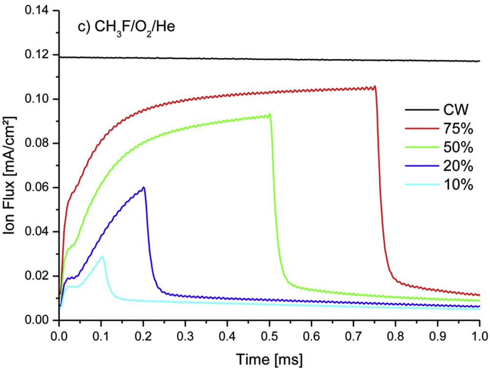
Time variation in the total positive ion flux in CH3FO2He plasma pulsed at 1 kHz for 75%, 50%, 20% and 10% dcs and continuous excitation (CW). Reproduced with permission from Blanc et al. [64]. Copyright 2014, AVS Publishing.
Fluorine-based plasmas have been recently proposed to achieve atom layer etching of Si3N4 in combination with an annealing step [66]. The principle is to induce a self-limited chemical conversion of the material into (NH4)2SiF6 salts as a result of the exposure to active species generated in a NH3NF3–based plasma. To avoid any damage due to ion bombardment the reaction chamber is located downstream with respect to the plasma chamber (remote plasma process). The modified layer (1–1.5 nm thick) is subsequently removed during the annealing. Such process is of great interest in fin field-effect transistor (FinFET) and gate all around technologies in which Si3N4 is a rather convenient mask material for the design of the Si fin [67]. A very highly selective removal of the Si3N4 mask with respect to the Si fin is necessary before deposition of the gate oxide and poly-Si gate materials.
3.2 Low-k interlevel dielectric etching
Low-k materials have been introduced as interlevel dielectrics in the place of SiO2 at the end of the 1990s, together with replacement of aluminium by copper for the metal lines. Objective was to decrease the parasite capacitor between two adjacent lines, thanks to the use of a low dielectric constant material. Choice of materials rapidly converged to porous methylsiloxane or methylsilsesquioxane compounds (p-SiOCH). In the integration scheme and besides control of the pattern dimension, etching lines and vias require a high selectivity towards the etch mask (SiO2), a high etch selectivity towards the bottom layer (SiCxHy diffusion barrier) and, most important, a low degradation of the material electrical properties. As the materials resemble to silicon oxide, etching recipe is thus based on fluorocarbon chemistry [68]. Within the last 20 years, a tremendous work has been carried out on the etching of porous low-k materials and on processes to seal the pattern or recovery of the dielectric performance [69]. The example presented hereafter is only a particular one, it has been chosen to illustrate the effect of a pulsed bias on fluorocarbon plasma. As shown in Fig. 12a and c, pattern transfer in CHF3 and CHF3–(25%)H2 (the latter to improve selectivity and anisotropy by favouring CFx deposition) with a substrate self-bias of 65 V is, in this case, rather deceiving. The main reason is the too low substrate bias (and ion energy) to obtain a correct pattern transfer. Yet, operating at a low substrate bias is compulsory because selectivity, which is low at high biases (∼2), is found to increase when the bias approaches the etching/deposition threshold [37]. Fig. 12b and d shows that operating with a pulsed bias brings a potential solution. During the bias OFF step CFx deposition occurs on both the SiO2 mask and p-SiOCH. As a result a higher bias is needed during the bias ON step because during this time the fluorocarbon layer needs to be removed quickly enough to allow material etching. As seen in Fig. 12b and d a very satisfying pattern transfer is achieved due to the combination of two effects. First, the deposition/etching threshold is at a higher bias for SiO2 and SiCxHy than for p-SiOCH [37], therefore a significantly large bias window exists in which infinite selectivity can be obtained; XPS analysis brings an explanation to this observation: due to its porosity, the p-SiOCH surface is much richer in fluorine than that of SiO2 or SiCxHy, which allows a much faster start of the etching when bias is applied [37]. Second, in this process window of infinite selectivity, the much higher net bias (110 V in CHF3–(25%)H2 at 0.5 dc, and 170 V in CHF3 at 0.25 dc) favours pattern anisotropy.

Line patterns etched in the porous methylsiloxane material in CHF3 (a and b) and CHF3–(25%)H2 (c and d) plasmas, the SiO2 mask was waived off when cleaving the sample for SEM observation (a,c) in CW bias (65 V), pulsed bias with dcs of 0.25 (CHF3—170 V) (b) and 0.5 (CHF3–(25%)H2—110 V) (d); pressure 5 mTorr, source power 1500 W and total gas flow 40 sccm.
4 Deep etching and etching materials for MEMS and MOEMS
4.1 Deep etching in silicon
Deep etching (5–500 μm) in silicon requires to operate with a high ER (>5 μm/min). This can only be obtained with a SF6-based chemistry because fluorine atoms will allow multilayer adsorption kinetic processes and SFx species will not form any blocking layer. Yet, patterning commands to suppress lateral etching and moreover to control the sidewall slope with a precision better that 1°. This means that sidewall passivation has to be mastered very efficiently. Two main processes have been developed.
4.1.1 SF6/C4F8-pulsed gas process
This pulsed gas process (also called the Bosch process [70] and initially proposed with SF6/CHF3) is based on the combination of an isotropic etching step (in SF6 plasma) and a deposition step (in C4F8 plasma) [39]. Ion bombardment at the pattern bottom during the etching step enables the removal of the fluorocarbon film and enhances downward etching (Fig. 13). Good pattern transfer, that is, perfect overall anisotropy, requires a fine adjustment of the two steps in terms of duration, gas flow and sample bias (etching step). Alternation of etching and deposition leads to a scalloped sidewall recovered with a thin fluorocarbon film.
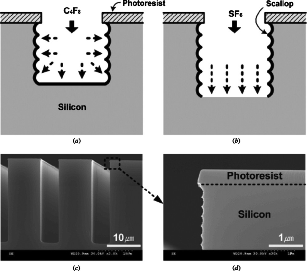
Principle of the SF6/C4F8 pulsed gas–etching process. Reproduced from Wu et al. [39]. Copyright 2010, AIP Publishing.
This process meets the requirements of Si MEMS fabrication and is used for most devices where deep features and high aspect ratio structures are needed. As an example Fig. 14 shows 3D microstructures realised as a support for microbatteries [71].
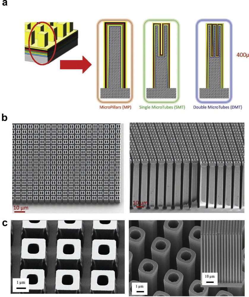
a) Concept of microbatteries based on Si micropillars, single microtubes, double microtubes; SEM images for (b) single microtubes and (c) double microtubes, photoresist mask prior etching (left) and Si etched structures (right). Reproduced with permission from Letiche et al. [71]. Copyright 2017, Wiley-VCH.
4.1.2 SF6O2 cryogenic process
The second operates in SF6O2 and is based on the combination of cryogenic temperature (∼−110 °C) [72] and the passivation of the sidewall owing to the formation of a SiOxFy layer [73]. Advantage is that the condensed species desorb when bringing the sample back to room temperature at the end of the process [74], leaving a chemically clean Si surface. However, the process window in temperature permitting overall control of the pattern slope is too narrow (±1°) to be implemented on large surfaces [75]. Moreover, undercut below the mask and bowing defects near the top of the feature are observed, respectively, due to the absence of passivation at the first moments of the etching and due to the ion bombardment that weakens the passivation near the top sidewall (Fig. 15) [76]. The SF6 and O2 flow rates need fine tuning: a too low O2 partial pressure will result in a weak passivation and lateral etching; on the contrary, an overpassivation situation is encountered if the O2 partial pressure is too high, which leads to needles at the bottom (black silicon) [77], and/or positive slopes that close the pattern, or to columnar microstructures [78]. Black silicon, if unwanted for deep etching, has interesting potential applications because of its very low reflectivity, highly developed surface and super hydrophobicity [79]. Coming back to etching, because the SF6O2 process is highly chemical, crystalline orientation–dependent etching phenomena can be observed whenever one of the following parameters is not tuned correctly with respect to the other parameters, namely, too low temperature, too low applied bias and too high pressure [80].
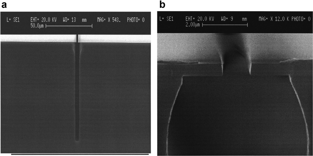
(a) Trench (2 μm wide, 80 μm deep) etched in the SF6O2 process at −90 °C, (b) enlargement of the trench top for a 1.2 μm wide trench, showing the undercut and bowing defects. Reproduced with permission from Aachboun and Ranson [76]. Copyright 1999, AVS Publishing.
Significant process improvement has been obtained by using alternated gas cycles (as in the Bosch process). Operated in SF6/SiF4/O2 or in SF6O2/SiF4/O2 the process builds the passivation layer not only on the condensation/oxidation reactions at the sidewall (in case of SF6O2 etching step) but also from the condensation of SiFx species (SiF4 plasma step) and their oxidation (O2 plasma step). The independent control of the passivation with respect to the etching step permits to obtain a much more robust process and an enlarged temperature window [75]. Moreover, the undercut and bowing defects are significantly reduced. The SF6/SiF4/O2 cycle process (10 s / 6 s / 6 s) leads, however, to a scalloped trench profile, and a 50% loss in the average ER as compared to the standard SF6O2 process because of the respective step times (Fig. 16). A better efficiency and a much smother profile are obtained with the SF6O2/SiF4/O2 cycle process (1 min / 7 s / 7 s) (Fig. 16).
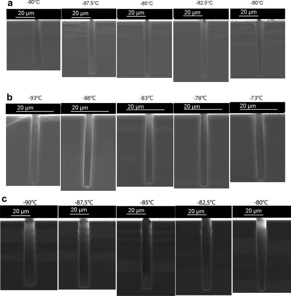
Comparison of SF6O2 (a), SF6/SiF4/O2 (b) and SF6O2/SiF4/O2 (c) cryoetching processes. Total process time is 10 min in each case. Reproduced with permission from Tillocher et al. [75]. Copyright 2008, the Electrochemical Society.
5 Surface functionalisation
One of the main applications is the grafting of fluorine species or the deposition of a fluorocarbon coating to modify the surface wettability [81]. The surface to be treated can be microstructured [82] or nanostructured [83]. Poly-methylmethacrylate (PMMA), for example, can be treated in O2 plasma to reduce its reflectivity and yet maintain a high transparency [84] and further coated with a fluorocarbon film (e.g., C4F8 plasma) to increase a water contact angle [85]. The same sequence of treatment carried out locally can be used to delimitate superhydrophobic regions in the superhydrophilic PMMA surface obtained after the O2 plasma, the latter can be used for local cell culture [86]. Using colloidal lithography (with polystyrene spheres) to generate hierarchical roughness micropillars (Fig. 17) in PMMA in O2 plasma, followed by a C4F8 plasma fluorocarbon coating, the ability to obtain superamphiphilic to superamphiphobic surfaces has been demonstrated (Fig. 18) [87].
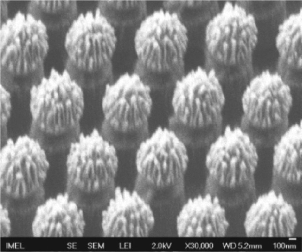
Hierarchical roughness micropillars produced by PMMA etching in O2 plasma using 1 μm PS spheres as etch mask. Reproduced with permission from Ellinas et al. [87]. Copyright 2011, ACS Publishing.
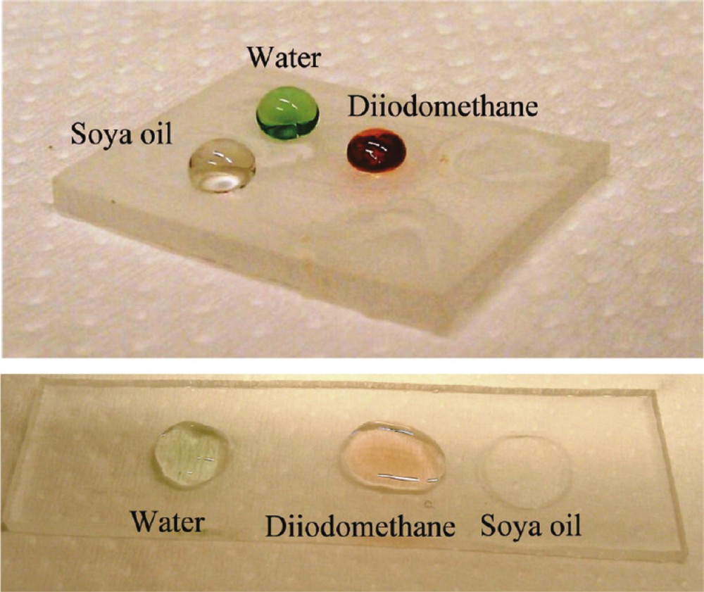
Top) Fluorocarbon-coated oxygen plasma treated superamphiphobic PMMA surface, (bottom) oxygen plasma treated superamphiphilic PMMA surface. Reproduced with permission from Ellinas et al. [87]. Copyright 2011, ACS Publishing.
The colloidal strategy for large area surface patterning can be used for other materials than polymers. As an example Fig. 19 shows the fabrication of steep micropillars in silicon using the SF6O2 cryogenic process [82].
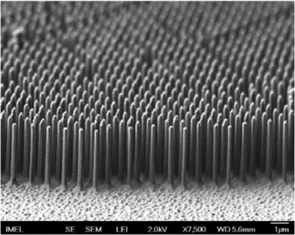
Silicon pillars (diameter 200 nm, aspect ratio 18:1) etched in cryogenic SF6O2 plasma using colloidal 1 μm PS spheres whose size had been first reduced in O2 plasma. Reproduced with permission from Ellinas et al. [82]. Copyright 2011, Elsevier.
6 Conclusions
Fluorine-based plasmas have been at the origin of the development of plasma processing for microelectronics and participated for a large part in the huge development of integrated devices and technology since 40 years, in increasingly wider domains of applications. The first main reason is the intrinsic properties of the fluorine atom and its ability to form volatile compounds with silicon-based materials. The second important reason is the variability of nondangerous gaseous molecular sources of fluorine atoms, which facilitates greatly technical implementation and process technology developments. The third reason, and not the least, is the large variability of plasma dissociation products obtained from these gaseous precursors, whose interaction with materials and surfaces allows fine surface engineering.
Naturally all this technology development has only been possible owing to human genius. Nowadays, domain of application mostly concerns microelectronics (Si-technology), micro- and nanotechnology devices and surface functionalisation. One can foresee that functionalisation is still in its infancy. Further studies need to be done for other applications, for example, in the field of nanoparticles and materials (synthesis and surface treatment).
Acknowledgements
The author is forever grateful to Professor Bernard Grolleau and Professor Guy Turban, who introduced him to plasma science and plasma etching. He also acknowledges former PhD students, Alain Campo, Thierry Chevolleau, Laëtitia Rolland, Freddy Gaboriau, David Eon, Vanessa Raballand, Ludovic Godet, Fanny Bailly and Ludovic Lallement, co-workers at IMN, Marie-Claude Peignon, Pierre-Yves Tessier, Gilles Cartry and Ahmed Rhallabi, as well as colleagues and collaborators from CEA-Leti, GREMI, LPSC, LTM, NSCR-Demokritos for their contribution to the building of his expertise in fluorine-based plasmas.


